 | Электронный компонент: CS8312YN8 | Скачать:  PDF PDF  ZIP ZIP |
⌐
Semiconductor Components Industries, LLC, 2001
March, 2001 ¡ Rev. 4
1
Publication Order Number:
CS8312/D
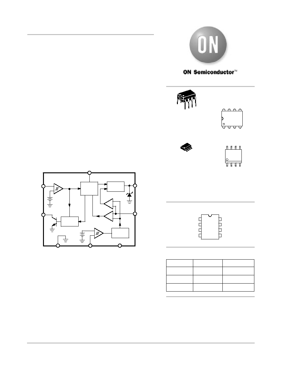
CS8312
IGBT Ignition Predriver with
Dynamic Current Regulation
The CS8312 is a bipolar microprocessor interface IC designed to
drive an IGBT (or logic level MOSFETs) powering large inductive
loads in harsh operating environments. The IC's dynamic current
limit function lets the microprocessor adjust the current limit threshold
to the real time needs of the system.
CLI, the current limit input, sets the current limit for the IGBT high
or low as directed by the system microprocessor. CLI also raises and
lowers the threshold on the diagnostic FLAG output signal. The
FLAG output signals the microprocessor when the current level
approaches current limit on the IGBT. The CTRL input enables the
FLAG function.
Features
╖
╡
P Compatible Inputs
╖
Adjustable Current Limit Thresholds
╖
External Sense Resistor
╖
Flag Signal to Indicate Output Status
Figure 1. Block Diagram
CTRL
FLAG
OUT
SENSE+
V
CC
SENSE¡
CLI
GND
Control
Logic
Latch
V
REF
Gate
Driver
V
T
V
T
5.0 V
http://onsemi.com
A
= Assembly Location
WL, L
= Wafer Lot
YY, Y
= Year
WW, W = Work Week
MARKING
DIAGRAMS
DIP¡8
N SUFFIX
CASE 626
1
8
Device
Package
Shipping
ORDERING INFORMATION
CS8312YN8
DIP¡8
50 Units/Rail
1
8
CS8312YN8
AWL
YYWW
OUT
GND
CLI
SENSE¡
CTRL
SENSE+
V
CC
FLAG
1
PIN CONNECTIONS
SO¡8
D SUFFIX
CASE 751
1
CS831
ALYW2
8
1
8
CS8312YD8
SO¡8
95 Units/Rail
CS8312YDR8
SO¡8
2500 Tape & Reel
CS8312
http://onsemi.com
2
ABSOLUTE MAXIMUM RATINGS*
Rating
Value
Unit
Supply Voltage
¡0.3 to 12
V
Digital Input Currents
2.0
mA
Internal Power Dissipation (T
A
= 25
░
C)
700
mW
Junction Temperature Range
¡40 to +150
░
C
Storage Temperature Range
¡55 to +165
░
C
Electrostatic Discharge (Human Body Model)
2.0
kV
Lead Temperature Soldering
Wave Solder (through hole styles only) Note 1.
Reflow (SMD styles only) Note 2.
260 peak
230 peak
░
C
░
C
1. 10 seconds max.
2. 60 seconds max above 183
░
C
*The maximum package power dissipation must be observed.
ELECTRICAL CHARACTERISTICS
(7.0 V
V
CC
10 V, ¡40
░
C
T
A
125
░
C,
¡0.2 V
Differential Ground Voltage
0.8 V; unless otherwise specified.)
Characteristic
Test Conditions
Min
Typ
Max
Unit
General
Power Supply Including Ripple Voltage
¡
7.0
¡
10
V
Supply Ripple Frequency
¡
10
¡
60
kHz
Differential Ground Frequency
¡
10
¡
60
kHz
Quiescent Current, I
Q
Turn On
Turn Off
V
CTRL
= 5.5 V
V
CTRL
= ¡0.3 V
¡
¡
¡
¡
15
5.0
mA
mA
Supply Voltage Rejection
V
CTRL
= 5.5 V
30
¡
¡
dB
Differential Ground Rejection Ratio
V
CTRL
= 5.5 V
30
¡
¡
dB
Differential Ground Current Ratio
V
CTRL
= ¡0.3 V,
(V
SENSE¡
¡ V
GND
)DC = 1.0 V
(V
SENSE¡
¡ V
GND
)AC = 0.6 V
¡
¡
3.0
mA
Unity Gain Bandwidth
V
CTRL
= 5.5 V
400
¡
¡
kHz
Turn On Delay
CTRL Increasing
¡
¡
30
╡
s
Turn Off Delay
CTRL Decreasing
¡
¡
30
╡
s
Control Function
Input Voltage Range
I
CTRL
= 2.0 mA
¡0.3
¡
5.5
V
Input Threshold
Turn On
Turn Off
Hysteresis
CTRL Increasing
CTRL Decreasing
¡
1.5
0.4
¡
¡
¡
3.5
¡
2.0
V
V
V
Voltage
I
CTRL
= 10
╡
A max
¡
¡
1.1
V
Input Capacitance
¡
¡
¡
50
pF
Current Limit Increase Function
Input Voltage Range
I
CTRL
= 2.0 mA
¡0.3
¡
5.5
V
Input Threshold
Turn On
Turn Off
Hysteresis
CLI Increasing
CLI Decreasing
¡
1.5
0.4
¡
¡
¡
3.5
¡
2.0
V
V
V
Voltage
I
CLI
= 10
╡
A max
¡
¡
1.1
V
CS8312
http://onsemi.com
3
ELECTRICAL CHARACTERISTICS (continued)
(7.0 V
V
CC
10 V, ¡40
░
C
T
A
125
░
C,
¡0.2 V
Differential Ground Voltage
0.8 V; unless otherwise specified.)
Characteristic
Unit
Max
Typ
Min
Test Conditions
Current Limit Increase Function (continued)
Input Capacitance
¡
¡
¡
50
pF
Output Stage
I
OUT
¡
¡
¡
5.0
mA
Clamp Voltage
V
CTRL
= 5.5 V, I
OUT
= 1.0 mA
4.0
¡
5.5
V
Output Off Voltage
V
CTRL
= ¡0.3 V, I
OUT
= 10
╡
A
V
CTRL
= ¡0.3 V, I
OUT
= 200
╡
A
¡
¡
¡
¡
0.5
1.2
V
V
Flag Function
Output Low
V
CTRL
= 5.5 V, I
FLAG
= 1.5 mA
¡
¡
0.9
V
Leakage Current
V
CTRL
= ¡0.3 V
¡
¡
10
╡
A
Output Capacitance
¡
¡
¡
50
pF
Turn On (V
SENSE+
¡ V
SENSE¡
)
V
CTRL
= 5.5 V, V
CLI
= ¡0.3 V
V
CTRL
= 5.5 V, V
CLI
= 5.5 V
210
300
225
¡
240
350
mV
mV
Turn Off Delay
CTRL Decreasing
¡
¡
10
╡
s
Turn On Delay
¡
¡
¡
10
╡
s
Disable Time
¡
100
¡
450
╡
s
Sense Function
Input Voltage Range
¡
¡0.3
¡
2.5
V
Sense Regulation Voltage
V
CTRL
= 5.5 V, V
CLI
= ¡0.3 V
V
CTRL
= 5.5 V, V
CLI
= 5.5 V
270
380
295
410
320
440
mV
mV
Input Leakage Current
V
CTRL
= 5.5 V
¡
¡
5.0
╡
A
Propagation Delay
V
CTRL
= 5.5 V
¡
¡
20
╡
s
PACKAGE PIN DESCRIPTION
PACKAGE PIN #
DIP¡8
SO¡8
PIN SYMBOL
FUNCTION
1
1
FLAG
Indicates whether current through the IGBT has reached a pre-
set level.
2
2
SENSE+
Positive input to current comparator.
3
3
SENSE¡
Ground (SENSE¡) for current sense resistor.
4
4
GND
Ground connection.
5
5
OUT
Output voltage to IGBT (MOSFET) gate.
6
6
CLI
Current limit input increase.
7
7
CTRL
Control input.
8
8
V
CC
Supply voltage.
CS8312
http://onsemi.com
4
CIRCUIT DESCRIPTION
Flag Function (See Figure 2)
The flag indicates when the voltage across the two sense
pins is approaching a current limit level that has been
determined by the value of the external sense resistor
(R
SENSE
) and the state of the CTRL and CLI pins. If the
voltage across the sense pins (SENSE+, SENSE¡) is less
than the flag turn¡on voltage, then the FLAG is off. When
the voltage between the sense pins equals the FLAG turn on
voltage, the FLAG will latch on until the CTRL pin goes
low. FLAG is disabled whenever CTRL is low. Changing the
CLI pin from low to high will increase nominal FLAG turn
on voltage by approximately 45%.
Table 1. FLAG Timing Sequence
State
CONTROL
SENSE+
FLAG
0
Low
X
OFF
1
High
Below Threshold
OFF
2
High
Above Threshold
ON
3
High
X
ON
0
Low
X
OFF
Output Stage
The CS8312 output (OUT) saturates and supplies voltage
to the IGBT (or MOSFET) gate once the CTRL switches
from low to high. As current through the IGBT (MOSFET)
increases and the voltage across the sense resistor passes the
flag turn on voltage, the FLAG will turn on. If the current
through the sense resistor continues to rise and the sense
resistor voltage reaches the regulation sense voltage, then
the gate voltage will fall to a level that regulates the driver
and maintains the regulation sense voltage at the sense
resistor.
Current Limit Function
Changing the CLI pin from a logic low to a logic high
increases the FLAG turn on voltage by approximately 45%
and the regulation sense voltage by approximately 39%
respectively.
Figure 2. Application and Test Diagram
FLAG
CTRL
CLI
OUT
SENSE+
SENSE¡
GND
V
CC
CS8312
Microprocessor
V
CC
R
V
CC
V
BAT
LOAD
R
SENSE
0.1
╡
F

CS8312
http://onsemi.com
5
PACKAGE DIMENSIONS
DIP¡8
N SUFFIX
CASE 626¡05
ISSUE L
NOTES:
1. DIMENSION L TO CENTER OF LEAD WHEN
FORMED PARALLEL.
2. PACKAGE CONTOUR OPTIONAL (ROUND OR
SQUARE CORNERS).
3. DIMENSIONING AND TOLERANCING PER ANSI
Y14.5M, 1982.
1
4
5
8
F
NOTE 2
¡A¡
¡B¡
¡T¡
SEATING
PLANE
H
J
G
D
K
N
C
L
M
M
A
M
0.13 (0.005)
B
M
T
DIM
MIN
MAX
MIN
MAX
INCHES
MILLIMETERS
A
9.40
10.16
0.370
0.400
B
6.10
6.60
0.240
0.260
C
3.94
4.45
0.155
0.175
D
0.38
0.51
0.015
0.020
F
1.02
1.78
0.040
0.070
G
2.54 BSC
0.100 BSC
H
0.76
1.27
0.030
0.050
J
0.20
0.30
0.008
0.012
K
2.92
3.43
0.115
0.135
L
7.62 BSC
0.300 BSC
M
---
10
---
10
N
0.76
1.01
0.030
0.040
_
_
SO¡8
D SUFFIX
CASE 751¡07
ISSUE W
SEATING
PLANE
1
4
5
8
N
J
X 45
_
K
NOTES:
1. DIMENSIONING AND TOLERANCING PER ANSI
Y14.5M, 1982.
2. CONTROLLING DIMENSION: MILLIMETER.
3. DIMENSION A AND B DO NOT INCLUDE MOLD
PROTRUSION.
4. MAXIMUM MOLD PROTRUSION 0.15 (0.006) PER
SIDE.
5. DIMENSION D DOES NOT INCLUDE DAMBAR
PROTRUSION. ALLOWABLE DAMBAR
PROTRUSION SHALL BE 0.127 (0.005) TOTAL IN
EXCESS OF THE D DIMENSION AT MAXIMUM
MATERIAL CONDITION.
A
B
S
D
H
C
0.10 (0.004)
DIM
A
MIN
MAX
MIN
MAX
INCHES
4.80
5.00
0.189
0.197
MILLIMETERS
B
3.80
4.00
0.150
0.157
C
1.35
1.75
0.053
0.069
D
0.33
0.51
0.013
0.020
G
1.27 BSC
0.050 BSC
H
0.10
0.25
0.004
0.010
J
0.19
0.25
0.007
0.010
K
0.40
1.27
0.016
0.050
M
0
8
0
8
N
0.25
0.50
0.010
0.020
S
5.80
6.20
0.228
0.244
¡X¡
¡Y¡
G
M
Y
M
0.25 (0.010)
¡Z¡
Y
M
0.25 (0.010)
Z
S
X
S
M
_
_
_
_
PACKAGE THERMAL DATA
Parameter
DIP¡8
SO¡8
Unit
R
JC
Typical
52
45
░
C/W
R
JA
Typical
100
165
░
C/W

CS8312
http://onsemi.com
6
Notes

CS8312
http://onsemi.com
7
Notes
CS8312
http://onsemi.com
8
ON Semiconductor and are trademarks of Semiconductor Components Industries, LLC (SCILLC). SCILLC reserves the right to make changes
without further notice to any products herein. SCILLC makes no warranty, representation or guarantee regarding the suitability of its products for any particular
purpose, nor does SCILLC assume any liability arising out of the application or use of any product or circuit, and specifically disclaims any and all liability,
including without limitation special, consequential or incidental damages. "Typical" parameters which may be provided in SCILLC data sheets and/or
specifications can and do vary in different applications and actual performance may vary over time. All operating parameters, including "Typicals" must be
validated for each customer application by customer's technical experts. SCILLC does not convey any license under its patent rights nor the rights of others.
SCILLC products are not designed, intended, or authorized for use as components in systems intended for surgical implant into the body, or other applications
intended to support or sustain life, or for any other application in which the failure of the SCILLC product could create a situation where personal injury or
death may occur. Should Buyer purchase or use SCILLC products for any such unintended or unauthorized application, Buyer shall indemnify and hold
SCILLC and its officers, employees, subsidiaries, affiliates, and distributors harmless against all claims, costs, damages, and expenses, and reasonable
attorney fees arising out of, directly or indirectly, any claim of personal injury or death associated with such unintended or unauthorized use, even if such claim
alleges that SCILLC was negligent regarding the design or manufacture of the part. SCILLC is an Equal Opportunity/Affirmative Action Employer.
PUBLICATION ORDERING INFORMATION
CENTRAL/SOUTH AMERICA:
Spanish Phone: 303¡308¡7143 (Mon¡Fri 8:00am to 5:00pm MST)
Email: ONlit¡spanish@hibbertco.com
Toll¡Free from Mexico: Dial 01¡800¡288¡2872 for Access ¡
then Dial 866¡297¡9322
ASIA/PACIFIC: LDC for ON Semiconductor ¡ Asia Support
Phone: 1¡303¡675¡2121 (Tue¡Fri 9:00am to 1:00pm, Hong Kong Time)
Toll Free from Hong Kong & Singapore:
001¡800¡4422¡3781
Email: ONlit¡asia@hibbertco.com
JAPAN: ON Semiconductor, Japan Customer Focus Center
4¡32¡1 Nishi¡Gotanda, Shinagawa¡ku, Tokyo, Japan 141¡0031
Phone: 81¡3¡5740¡2700
Email: r14525@onsemi.com
ON Semiconductor Website: http://onsemi.com
For additional information, please contact your local
Sales Representative.
CS8312/D
NORTH AMERICA Literature Fulfillment:
Literature Distribution Center for ON Semiconductor
P.O. Box 5163, Denver, Colorado 80217 USA
Phone: 303¡675¡2175 or 800¡344¡3860 Toll Free USA/Canada
Fax: 303¡675¡2176 or 800¡344¡3867 Toll Free USA/Canada
Email: ONlit@hibbertco.com
Fax Response Line: 303¡675¡2167 or 800¡344¡3810 Toll Free USA/Canada
N. American Technical Support: 800¡282¡9855 Toll Free USA/Canada
EUROPE: LDC for ON Semiconductor ¡ European Support
German Phone: (+1) 303¡308¡7140 (Mon¡Fri 2:30pm to 7:00pm CET)
Email: ONlit¡german@hibbertco.com
French Phone: (+1) 303¡308¡7141 (Mon¡Fri 2:00pm to 7:00pm CET)
Email: ONlit¡french@hibbertco.com
English Phone: (+1) 303¡308¡7142 (Mon¡Fri 12:00pm to 5:00pm GMT)
Email: ONlit@hibbertco.com
EUROPEAN TOLL¡FREE ACCESS*: 00¡800¡4422¡3781
*Available from Germany, France, Italy, UK, Ireland