 | –≠–ª–µ–∫—Ç—Ä–æ–Ω–Ω—ã–π –∫–æ–º–ø–æ–Ω–µ–Ω—Ç: MBR350RL | –°–∫–∞—á–∞—Ç—å:  PDF PDF  ZIP ZIP |

©
Semiconductor Components Industries, LLC, 2004
December, 2004 - Rev. 4
1
Publication Order Number:
MBR350/D
MBR350, MBR360
MBR360 is a Preferred Device
Axial Lead Rectifiers
These devices employ the Schottky Barrier principle in a large area
metal-to-silicon power diode. State-of-the-art geometry features
epitaxial construction with oxide passivation and metal overlap
contact. Ideally suited for use as rectifiers in low-voltage,
high-frequency inverters, free wheeling diodes, and polarity
protection diodes.
Features
∑
Extremely Low v
F
∑
Low Power Loss/High Efficiency
∑
Highly Stable Oxide Passivated Junction
∑
Low Stored Charge, Majority Carrier Conduction
∑
Shipped in plastic bags, 500 per bag
∑
Available Tape and Reeled, 1500 per reel, by adding a "RL'' suffix to
the part number
∑
These devices are manufactured with a Pb-Free external lead
finish only*
Mechanical Characteristics:
∑
Case: Epoxy, Molded
∑
Weight: 1.1 gram (approximately)
∑
Finish: All External Surfaces Corrosion Resistant and Terminal
Leads are Readily Solderable
∑
Lead and Mounting Surface Temperature for Soldering Purposes:
220
∞
C Max. for 10 Seconds, 1/16 in from case
∑
Polarity: Cathode indicated by Polarity Band
MAXIMUM RATINGS
Rating
Symbol
Max
Unit
Peak Repetitive Reverse Voltage
Working Peak Reverse Voltage
DC Blocking Voltage
MBR350
MBR360
V
RRM
V
RWM
V
R
50
60
V
Average Rectified Forward Current
T
A
= 65
∞
C (R
q
JA
= 28
∞
C/W,
P.C. Board Mounting)
I
O
3.0
A
Non-Repetitive Peak Surge Current
(Note 1) (Surge Applied at Rated Load
Conditions Halfwave, Single Phase,
60 Hz, T
L
= 75
∞
C)
I
FSM
80
A
Operating and Storage Junction
Temperature Range
(Reverse Voltage Applied)
T
J
, T
stg
-65 to +150
∞
C
Peak Operating Junction Temperature
(Forward Current Applied)
T
J(pk)
150
∞
C
Maximum ratings are those values beyond which device damage can occur.
Maximum ratings applied to the device are individual stress limit values (not
normal operating conditions) and are not valid simultaneously. If these limits
are exceeded, device functional operation is not implied, damage may occur
and reliability may be affected.
1. Lead Temperature reference is cathode lead 1/32 in from case.
*For additional information on our Pb-Free strategy and soldering details, please
download the ON Semiconductor Soldering and Mounting Techniques
Reference Manual, SOLDERRM/D.
Device
Package
Shipping
ORDERING INFORMATION
AXIAL LEAD
CASE 267-05
(DO-201AD)
STYLE 1
SCHOTTKY BARRIER
RECTIFIERS
3.0 AMPERES
50, 60 VOLTS
Preferred devices are recommended choices for future use
and best overall value.
MBR350
Axial Lead
500 Units/Bag
MBR350RL
Axial Lead
1500/Tape & Reel
MBR360
Axial Lead
500 Units/Bag
MBR360RL
Axial Lead
1500/Tape & Reel
MARKING DIAGRAM
MBR
3x0
MBR3x0= Device Code
x
= 5 or 6
For information on tape and reel specifications,
including part orientation and tape sizes, please
refer to our Tape and Reel Packaging Specifications
Brochure, BRD8011/D.
http://onsemi.com

MBR350, MBR360
http://onsemi.com
2
THERMAL CHARACTERISTICS
Characteristic
Symbol
Max
Unit
Thermal Resistance, Junction-to-Ambient (see Note 4, Mounting Method 3)
R
q
JA
28
∞
C/W
ELECTRICAL CHARACTERISTICS
(T
L
= 25
∞
C unless otherwise noted) (Note 2)
Characteristic
Symbol
Max
Unit
Maximum Instantaneous Forward Voltage (Note 3)
(i
F
= 1.0 Amp)
(i
F
= 3.0 Amp)
(i
F
= 9.4 Amp)
v
F
0.600
0.740
1.080
V
Maximum Instantaneous Reverse Current @ Rated dc Voltage (Note 3)
T
L
= 25
∞
C
T
L
= 100
∞
C
i
R
0.60
20
mA
2. Lead Temperature reference is cathode lead 1/32 in from case.
3. Pulse Test: Pulse Width = 300
m
s, Duty Cycle = 2.0%.
T
A
, AMBIENT TEMPERATURE (C
∞
)
20
100
60
40
80
4.0
2.0
3.0
5.0
0
1.0
DC
SQUARE
WAVE
120
140
160
I ,
A
VERAGE FOR
W
ARD CURRENT
(AMPS)
F (A
V)
V
R
REVERSE VOLTAGE (VOLTS)
0
20
10
30
40
0.002
0.005
0.01
0.05
0.02
0.10
0.50
0.20
20
10
5.0
2.0
1.0
25
∞
C
v
F,
INSTANTANEOUS VOLTAGE (VOLTS)
0.2
0
0.4
5.0
0.03
0.02
0.07
0.2
0.1
20
10
3.0
2.0
1.0
0.6
0.8
0.3
0.05
0.5
0.7
I , REVERSE CURRENT
(mA)
R
7.0
i , INST
ANT
ANEOUS FOR
W
ARD CURRENT
(AMPS)
F
1.0
1.2
1.4
*The curves shown are typical for the highest
voltage device in the voltage grouping. Typical
reverse current for lower voltage selections can
be estimated from these same curves if V
R
is
sufficiently below rated V
R
.
50
60
80
75
∞
C
100
∞
C
T
J
= 150
∞
C
T
J
= 100
∞
C
25
∞
C
75
∞
C
T
J
= 150
∞
C
RATED V
R
R
qJA
= 28
∞
C/W
0
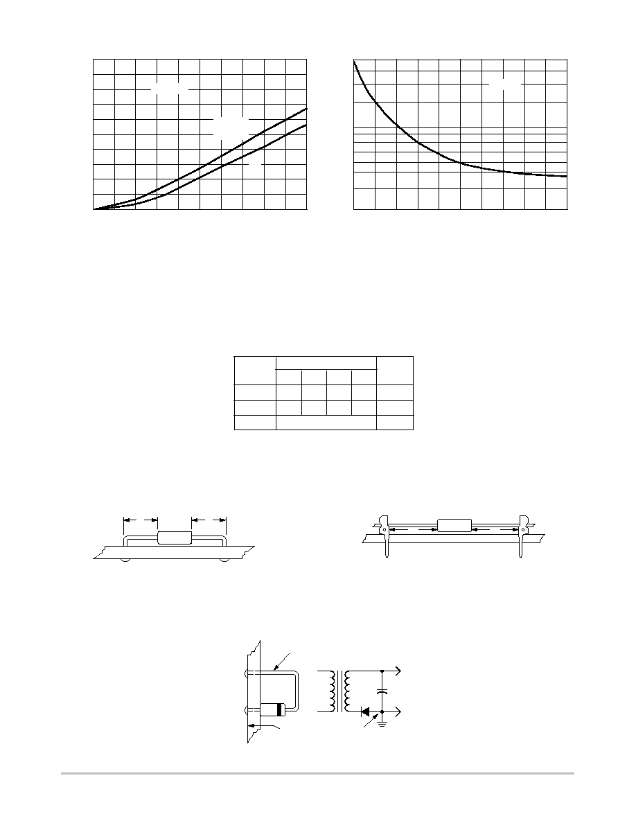
Figure 1. Typical Forward Voltage
Figure 2. Typical Reverse Current*
Figure 3. Current Derating Ambient
(Mounting Method #3 per Note 4)
MBR350, MBR360
http://onsemi.com
3
V
R
, REVERSE VOLTAGE (VOLTS)
I
F (AV)
, AVERAGE FORWARD CURRENT (AMPS)
0
2.0
1.0
3.0
4.0
5.0
1.0
2.0
3.0
4.0
5.0
T
J
= 150
∞
C
P
,
A
VERAGE POWER DISSIP
A
TION (W
A
TTS)
F (A
V)
dc
SQUARE
WAVE
0
20
10
30
40
50
70
300
T
J
= 25
∞
C
C, CAP
ACIT
ANCE (pF)
200
40
30
50
100
Figure 4. Power Dissipation
Figure 5. Typical Capacitance
0
TYPICAL VALUES FOR R
q
JA
IN STILL AIR
Data shown for thermal resistance junction-to-ambient
(R
qJA
) for the mountings shown is to be used as typical
guideline values for preliminary engineering, or in case the
tie point temperature cannot be measured.
1
2
3
Mounting
Method
Lead Length, L (in)
1/8
1/4
1/2
3/4
R
q
JA
50
51
53
55
∞
C/W
∞
C/W
∞
C/W
58
59
61
63
28
NOTE 4 -- MOUNTING DATA
……………………………
……………………………
…………………………………
…………………………………
……
……
……
……
……
……
……
Mounting Method 1
P.C. Board where available
copper surface is small.
L
L
L
Mounting Method 2
Vector Push-In
Terminals T-28
L
Mounting Method 3
P.C. Board with
2-1/2
X 2-1/2
copper surface.
L = 1/2''
Board Ground Plane
MBR350, MBR360
http://onsemi.com
4
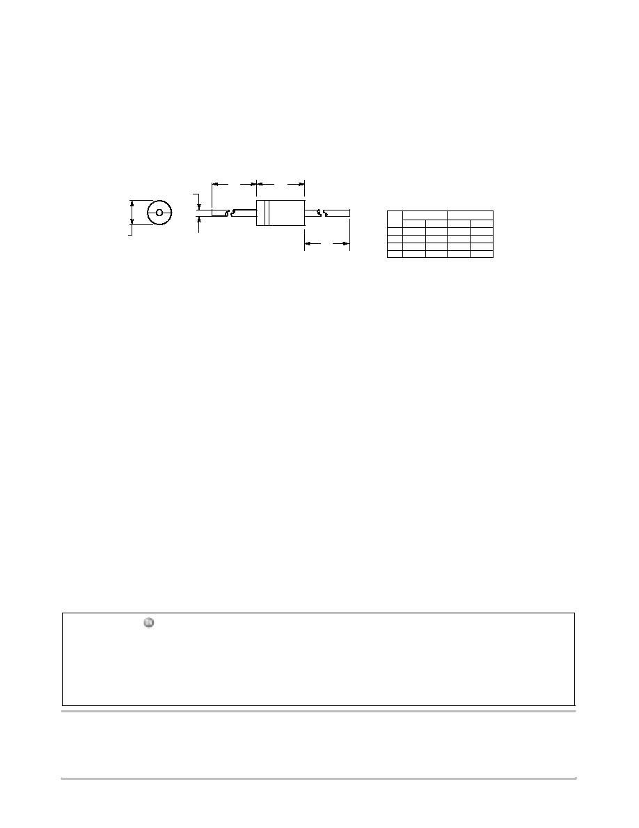
PACKAGE DIMENSIONS
AXIAL LEAD
CASE 267-05
(DO-201AD)
ISSUE G
NOTES:
1. DIMENSIONING AND TOLERANCING PER ANSI
Y14.5M, 1982.
2. CONTROLLING DIMENSION: INCH.
STYLE 1:
PIN 1. CATHODE (POLARITY BAND)
2. ANODE
1
2
K
A
K
D
B
DIM
MIN
MAX
MIN
MAX
MILLIMETERS
INCHES
A
0.287
0.374
7.30
9.50
B
0.189
0.209
4.80
5.30
D
0.047
0.051
1.20
1.30
K
1.000
---
25.40
---
ON Semiconductor and are registered trademarks of Semiconductor Components Industries, LLC (SCILLC). SCILLC reserves the right to make changes without further notice
to any products herein. SCILLC makes no warranty, representation or guarantee regarding the suitability of its products for any particular purpose, nor does SCILLC assume any liability
arising out of the application or use of any product or circuit, and specifically disclaims any and all liability, including without limitation special, consequential or incidental damages.
"Typical" parameters which may be provided in SCILLC data sheets and/or specifications can and do vary in different applications and actual performance may vary over time. All
operating parameters, including "Typicals" must be validated for each customer application by customer's technical experts. SCILLC does not convey any license under its patent rights
nor the rights of others. SCILLC products are not designed, intended, or authorized for use as components in systems intended for surgical implant into the body, or other applications
intended to support or sustain life, or for any other application in which the failure of the SCILLC product could create a situation where personal injury or death may occur. Should
Buyer purchase or use SCILLC products for any such unintended or unauthorized application, Buyer shall indemnify and hold SCILLC and its officers, employees, subsidiaries, affiliates,
and distributors harmless against all claims, costs, damages, and expenses, and reasonable attorney fees arising out of, directly or indirectly, any claim of personal injury or death
associated with such unintended or unauthorized use, even if such claim alleges that SCILLC was negligent regarding the design or manufacture of the part. SCILLC is an Equal
Opportunity/Affirmative Action Employer. This literature is subject to all applicable copyright laws and is not for resale in any manner.
PUBLICATION ORDERING INFORMATION
N. American Technical Support: 800-282-9855 Toll Free
USA/Canada
Japan: ON Semiconductor, Japan Customer Focus Center
2-9-1 Kamimeguro, Meguro-ku, Tokyo, Japan 153-0051
Phone: 81-3-5773-3850
MBR350/D
LITERATURE FULFILLMENT:
Literature Distribution Center for ON Semiconductor
P.O. Box 61312, Phoenix, Arizona 85082-1312 USA
Phone: 480-829-7710 or 800-344-3860 Toll Free USA/Canada
Fax: 480-829-7709 or 800-344-3867 Toll Free USA/Canada
Email: orderlit@onsemi.com
ON Semiconductor Website: http://onsemi.com
Order Literature: http://www.onsemi.com/litorder
For additional information, please contact your
local Sales Representative.