 | Электронный компонент: MBRS320T3 | Скачать:  PDF PDF  ZIP ZIP |
⌐
Semiconductor Components Industries, LLC, 2000
October, 2000 ¡ Rev. 3
1
Publication Order Number:
MBRS340T3/D
MBRS320T3, MBRS330T3,
MBRS340T3, MBRS360T3
Preferred Devices
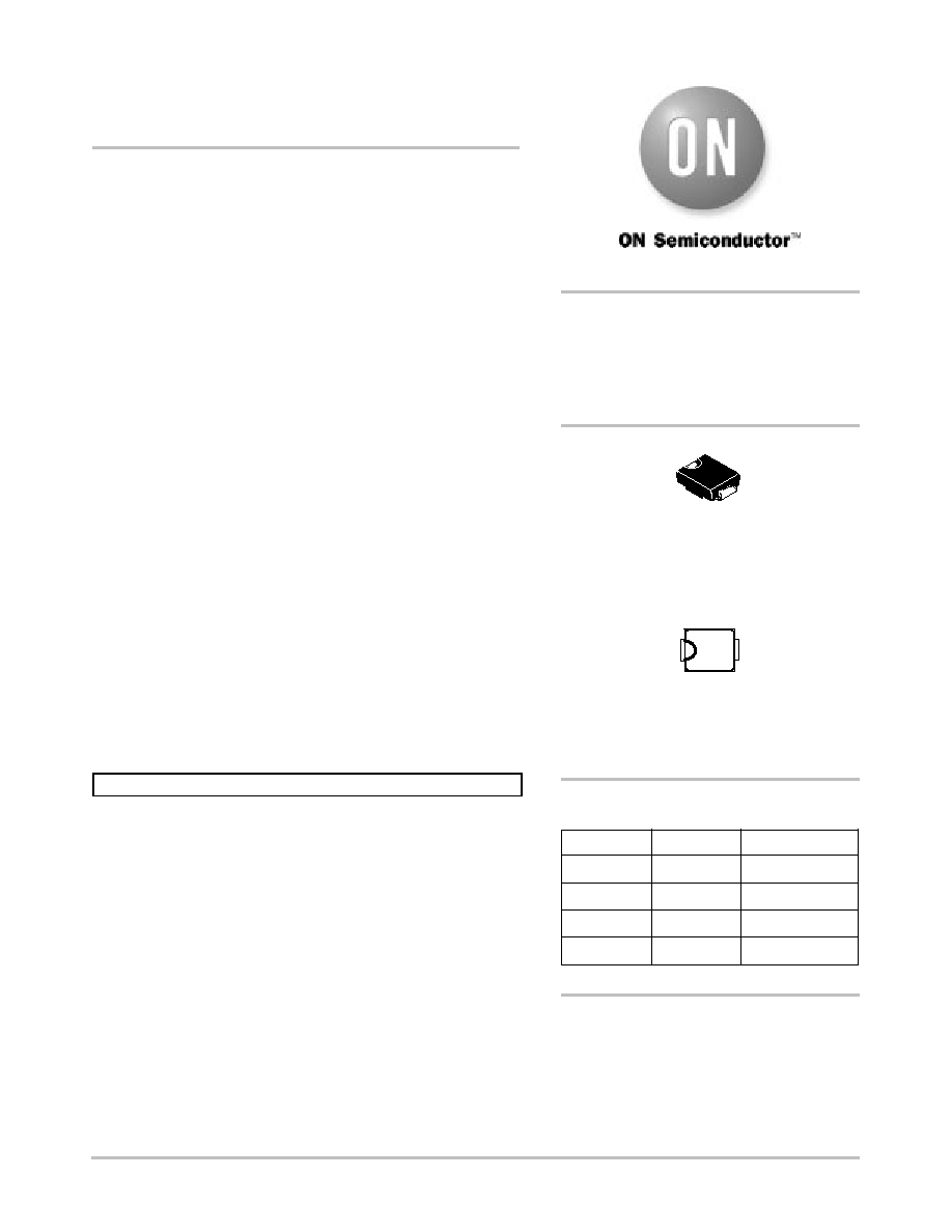
Surface Mount
Schottky Power Rectifier
. . . employing the Schottky Barrier principle in a large area
metal¡to¡silicon power diode. State¡of¡the¡art geometry features
epitaxial construction with oxide passivation and metal overlay
contact. Ideally suited for low voltage, high frequency rectification, or
as free wheeling and polarity protection diodes, in surface mount
applications where compact size and weight are critical to the system.
╖
Small Compact Surface Mountable Package with J¡Bend Leads
╖
Rectangular Package for Automated Handling
╖
Highly Stable Oxide Passivated Junction
╖
Very Low Forward Voltage Drop
(0.5 Volts Max @ 3.0 A, T
J
= 25
░
C)
╖
Excellent Ability to Withstand Reverse Avalanche Energy Transients
╖
Guardring for Stress Protection
Mechanical Characteristics:
╖
Case: Epoxy, Molded
╖
Weight: 217 mg (approximately)
╖
Finish: All External Surfaces Corrosion Resistant and Terminal
Leads are Readily Solderable
╖
Lead and Mounting Surface Temperature for Soldering Purposes:
260
░
C Max. for 10 Seconds
╖
Shipped in 16 mm Tape and Reel, 2500 units per reel
╖
Polarity: Notch in Plastic Body Indicates Cathode Lead
╖
Marking: B32, B33, B34, B36
MAXIMUM RATINGS
Please See the Table on the Following Page
Device
Package
Shipping
ORDERING INFORMATION
SMC
CASE 403
PLASTIC
http://onsemi.com
MBRS320T3
SMC
2500/Tape & Reel
SCHOTTKY BARRIER
RECTIFIERS
3.0 AMPERES
20, 30, 40, 60 VOLTS
Preferred devices are recommended choices for future use
and best overall value.
MBRS330T3
SMC
2500/Tape & Reel
MBRS340T3
SMC
2500/Tape & Reel
MBRS360T3
SMC
2500/Tape & Reel
MARKING DIAGRAM
YWW
B3x
B3x = Device Code
x
= 2, 3, 4 or 6
Y
= Year
W
= Work Week

MBRS320T3, MBRS330T3, MBRS340T3, MBRS360T3
http://onsemi.com
2
MAXIMUM RATINGS
Rating
Symbol
MBRS320T3
MBRS330T3
MBRS340T3
MBRS360T3
Unit
Peak Repetitive Reverse Voltage
Working Peak Reverse Voltage
DC Blocking Voltage
V
RRM
V
RWM
V
R
20
30
40
60
Volts
Average Rectified Forward Current
I
F(AV)
3.0 @ T
L
= 100
░
C
4.0 @ T
L
= 90
░
C
Amps
Nonrepetitive Peak Surge Current
(Surge applied at rated load conditions halfwave,
single phase, 60 Hz)
I
FSM
80
80
80
80
Amps
Operating Junction Temperature
T
J
¡ 65 to +125
¡ 65 to +125
¡ 65 to +125
░
C
THERMAL CHARACTERISTICS
Thermal Resistance -- Junction to Lead
R
JL
11
11
11
11
░
C/W
ELECTRICAL CHARACTERISTICS
Maximum Instantaneous Forward Voltage (Note 1.)
(i
F
= 3.0 A, T
J
= 25
░
C)
V
F
0.50
0.50
0.525
0.740
Volts
Maximum Instantaneous Reverse Current (Note 1.)
(Rated dc Voltage, T
J
= 25
░
C)
(Rated dc Voltage, T
J
= 100
░
C)
i
R
2.0
20
2.0
20
2.0
20
0.5
20
mA
1. Pulse Test: Pulse Width = 300
╡
s, Duty Cycle
2.0%.

MBRS320T3, MBRS330T3, MBRS340T3, MBRS360T3
http://onsemi.com
3
i F
, INST
ANT
ANEOUS FOR
W
ARD CURRENT
(AMPS)
1
0.5
0.2
0.1
0.05
3
2
1
0.1 0.2 0.3 0.4 0.5 0.6 0.7
v
F
, INSTANTANEOUS VOLTAGE (VOLTS)
Figure 1. Typical Forward Voltage
I R
, REVERSE CURRENT
(mA)
100
10
1
0.1
0.01 0
4
8
12
16
20
24
28
32
36
40
V
R
, REVERSE VOLTAGE (VOLTS)
Figure 2. Typical Reverse Current
T
J
= 125
░
C
25
░
C
T
J
= 100
░
C
P F(A
V)
,
A
VERAGE POWER DISSIP
A
TION (W
A
TTS) 5
4
3
2
1
0
0
1
2
3
4
5
I
F(AV)
, AVERAGE FORWARD CURRENT (AMPS)
Figure 3. Power Dissipation
= 20
10
5
DC
I
PK
I
AV
SQUARE
WAVE
20
2
0.2
0.02
50
5
0.5
0.05
(CAPACITIVE LOAD)
0.7
0.07
0.3
0.8 0.9
1.1
T
C
= 100
░
C
T
C
= 25
░
C
100
░
C
75
░
C
1.2 1.3 1.4
0
I F(A
V)
,
A
VERAGE FOR
W
ARD CURRENT
(AMPS)
8
7
6
5
4
3
2
1
0
50
60
70
80
90
100
110
120 130
T
C
, CASE TEMPERATURE (
░
C)
SQUARE
WAVE
DC
RATED VOLTAGE APPLIED
R
JC
= 10.5
░
C/W
T
J
= 125
░
C
C, CAP
ACIT
ANCE (pF)
400
300
200
100
0
0
4
8
12
16
20
24
28
32
V
R
, REVERSE VOLTAGE (VOLTS)
TYPICAL CAPACITANCE AT 0 V = 480 pF
36
40
500
40
140
9
10
Figure 4. Current Derating (Case)
Figure 5. Typical Capacitance
T
J
= 25
░
C
MBRS320T3, MBRS330T3, MBRS340T3, MBRS360T3
http://onsemi.com
4
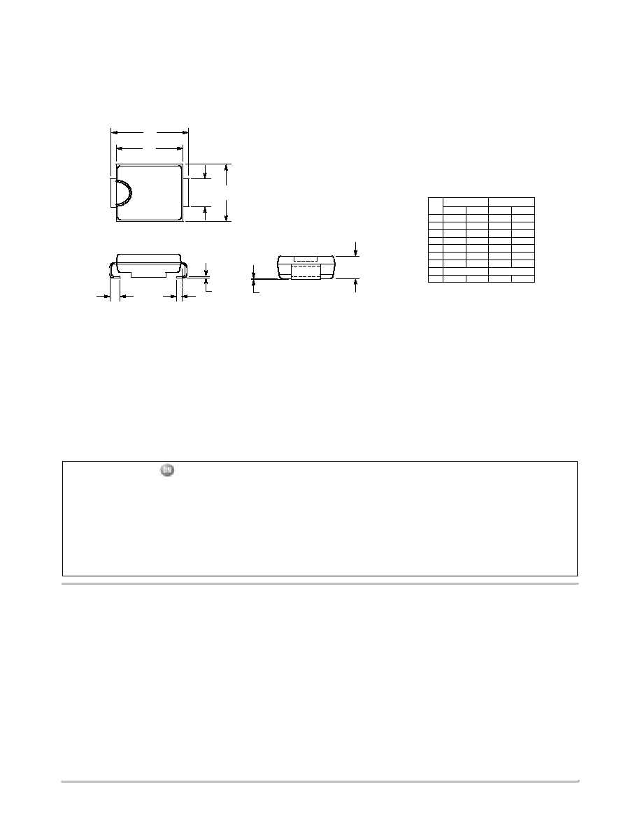
PACKAGE DIMENSIONS
SMC
PLASTIC PACKAGE
CASE 403¡03
ISSUE B
S
A
D
B
J
P
K
H
C
DIM
MIN
MAX
MIN
MAX
MILLIMETERS
INCHES
A
0.260
0.280
6.60
7.11
B
0.220
0.240
5.59
6.10
C
0.075
0.095
1.90
2.41
D
0.115
0.121
2.92
3.07
H 0.0020 0.0060
0.051
0.152
J
0.006
0.012
0.15
0.30
K
0.030
0.050
0.76
1.27
P
0.020 REF
0.51 REF
S
0.305
0.320
7.75
8.13
NOTES:
1. DIMENSIONING AND TOLERANCING PER ANSI
Y14.5M, 1982.
2. CONTROLLING DIMENSION: INCH.
3. D DIMENSION SHALL BE MEASURED WITHIN
DIMENSION P.
ON Semiconductor and are trademarks of Semiconductor Components Industries, LLC (SCILLC). SCILLC reserves the right to make changes
without further notice to any products herein. SCILLC makes no warranty, representation or guarantee regarding the suitability of its products for any particular
purpose, nor does SCILLC assume any liability arising out of the application or use of any product or circuit, and specifically disclaims any and all liability,
including without limitation special, consequential or incidental damages. "Typical" parameters which may be provided in SCILLC data sheets and/or
specifications can and do vary in different applications and actual performance may vary over time. All operating parameters, including "Typicals" must be
validated for each customer application by customer's technical experts. SCILLC does not convey any license under its patent rights nor the rights of others.
SCILLC products are not designed, intended, or authorized for use as components in systems intended for surgical implant into the body, or other applications
intended to support or sustain life, or for any other application in which the failure of the SCILLC product could create a situation where personal injury or
death may occur. Should Buyer purchase or use SCILLC products for any such unintended or unauthorized application, Buyer shall indemnify and hold
SCILLC and its officers, employees, subsidiaries, affiliates, and distributors harmless against all claims, costs, damages, and expenses, and reasonable
attorney fees arising out of, directly or indirectly, any claim of personal injury or death associated with such unintended or unauthorized use, even if such claim
alleges that SCILLC was negligent regarding the design or manufacture of the part. SCILLC is an Equal Opportunity/Affirmative Action Employer.
PUBLICATION ORDERING INFORMATION
CENTRAL/SOUTH AMERICA:
Spanish Phone: 303¡308¡7143 (Mon¡Fri 8:00am to 5:00pm MST)
Email: ONlit¡spanish@hibbertco.com
Toll¡Free from Mexico: Dial 01¡800¡288¡2872 for Access ¡
then Dial 866¡297¡9322
ASIA/PACIFIC: LDC for ON Semiconductor ¡ Asia Support
Phone: 303¡675¡2121 (Tue¡Fri 9:00am to 1:00pm, Hong Kong Time)
Toll Free from Hong Kong & Singapore:
001¡800¡4422¡3781
Email: ONlit¡asia@hibbertco.com
JAPAN: ON Semiconductor, Japan Customer Focus Center
4¡32¡1 Nishi¡Gotanda, Shinagawa¡ku, Tokyo, Japan 141¡0031
Phone: 81¡3¡5740¡2700
Email: r14525@onsemi.com
ON Semiconductor Website: http://onsemi.com
For additional information, please contact your local
Sales Representative.
MBRS340T3/D
NORTH AMERICA Literature Fulfillment:
Literature Distribution Center for ON Semiconductor
P.O. Box 5163, Denver, Colorado 80217 USA
Phone: 303¡675¡2175 or 800¡344¡3860 Toll Free USA/Canada
Fax: 303¡675¡2176 or 800¡344¡3867 Toll Free USA/Canada
Email: ONlit@hibbertco.com
Fax Response Line: 303¡675¡2167 or 800¡344¡3810 Toll Free USA/Canada
N. American Technical Support: 800¡282¡9855 Toll Free USA/Canada
EUROPE: LDC for ON Semiconductor ¡ European Support
German Phone: (+1) 303¡308¡7140 (Mon¡Fri 2:30pm to 7:00pm CET)
Email: ONlit¡german@hibbertco.com
French Phone: (+1) 303¡308¡7141 (Mon¡Fri 2:00pm to 7:00pm CET)
Email: ONlit¡french@hibbertco.com
English Phone: (+1) 303¡308¡7142 (Mon¡Fri 12:00pm to 5:00pm GMT)
Email: ONlit@hibbertco.com
EUROPEAN TOLL¡FREE ACCESS*: 00¡800¡4422¡3781
*Available from Germany, France, Italy, UK, Ireland