
©
Semiconductor Components Industries, LLC, 2000
October, 2000 ≠ Rev. 3
1
Publication Order Number:
MC10EL52/D
MC10EL52, MC100EL52
5V ECL Differential Data
and Clock D Flip Flop
The MC10EL/100EL52 is a differential data, differential clock D
flip-flop with reset. The device is functionally equivalent to the E452
device with higher performance capabilities. With propagation delays and
output transition times significantly faster than the E452, the EL52 is
ideally suited for those applications which require the ultimate in AC
performance.
Data enters the master portion of the flip-flop when the clock is LOW
and is transferred to the slave, and thus the outputs, upon a positive
transition of the clock. The differential clock inputs of the EL52 allow the
device to also be used as a negative edge triggered device.
The EL52 employs input clamping circuitry so that under open input
conditions (pulled down to V
EE
) the outputs of the device will remain
stable.
The 100 Series contains temperature compensation.
∑
365 ps Propagation Delay
∑
2.0 GHz Toggle Frequency
∑
ESD Protection: > 1 KV HBM, > 100 V MM
∑
PECL Mode Operating Range: V
CC
= 4.2 V to 5.7 V
with V
EE
= 0 V
∑
NECL Mode Operating Range: V
CC
= 0 V
with V
EE
= ≠4.2 V to ≠5.7 V
∑
Internal Input Pulldown Resistors on D and CLK
∑
Meets or Exceeds JEDEC Spec EIA/JESD78 IC Latchup Test
∑
Moisture Sensitivity Level 1
For Additional Information, see Application Note AND8003/D
∑
Flammability Rating: UL≠94 code V≠0 @ 1/8",
Oxygen Index 28 to 34
∑
Transistor Count = 48 devices
http://onsemi.com
Device
Package
Shipping
ORDERING INFORMATION
MC10EL52D
SO≠8
98 Units/Rail
MC10EL52DR2
SO≠8
2500 Tape & Reel
MC100EL52D
SO≠8
98 Units/Rail
MC100EL52DR2
SO≠8
2500 Tape & Reel
MC10EL52DT
TSSOP≠8
98 Units/Rail
MC10EL52DTR2
TSSOP≠8 2500 Tape & Reel
MC100EL52DT
TSSOP≠8
98 Units/Rail
MC100EL52DTR2
TSSOP≠8 2500 Tape & Reel
L = Wafer Lot
Y = Year
W = Work Week
*For additional information, see Application Note
AND8002/D
H = MC10
K = MC100
A = Assembly Location
SO≠8
D SUFFIX
CASE 751
MARKING
DIAGRAMS*
TSSOP≠8
DT SUFFIX
CASE 948R
1
8
1
8
ALYW
KEL52
1
8
HEL52
1
8
ALYW
ALYW
HL52
1
8
ALYW
KL52
1
8

MC10EL52, MC100EL52
http://onsemi.com
2
LOGIC DIAGRAM AND PINOUT ASSIGNMENT
1
2
3
4
5
6
7
8
Q
V
EE
V
CC
D
Q
CLK
CLK
D
D
TRUTH TABLE
D*
L
H
CLK*
Z
Z
Q
L
H
Z = LOW to HIGH Transition
D, D
ECL Data Input
CLK, CLK
ECL Clock Input
Q, Q
ECL Data Output
V
CC
Positive Supply
V
EE
Negative Supply
PIN DESCRIPTION
PIN
FUNCTION
* Pin will default low when left open.
MAXIMUM RATINGS
(Note 1.)
Symbol
Parameter
Condition 1
Condition 2
Rating
Units
V
CC
PECL Mode Power Supply
V
EE
= 0 V
8
V
V
EE
NECL Mode Power Supply
V
CC
= 0 V
≠8
V
V
I
PECL Mode Input Voltage
V
EE
= 0 V
V
I
V
CC
6
V
I
C
ode
u
o age
NECL Mode Input Voltage
EE
0
V
CC
= 0 V
I
CC
V
I
V
EE
6
≠6
V
I
out
Output Current
Continuous
Surge
50
100
mA
mA
TA
Operating Temperature Range
≠40 to +85
∞
C
T
stg
Storage Temperature Range
≠65 to +150
∞
C
JA
Thermal Resistance (Junction to Ambient)
0 LFPM
500 LFPM
8 SOIC
8 SOIC
190
130
∞
C/W
∞
C/W
JC
Thermal Resistance (Junction to Case)
std bd
8 SOIC
41 to 44
∞
C/W
JA
Thermal Resistance (Junction to Ambient)
0 LFPM
500 LFPM
8 TSSOP
8 TSSOP
185
140
∞
C/W
∞
C/W
JC
Thermal Resistance (Junction to Case)
std bd
8 TSSOP
41 to 44
±
5%
∞
C/W
T
sol
Wave Solder
<2 to 3 sec @ 248
∞
C
265
∞
C
1. Maximum Ratings are those values beyond which device damage may occur.

MC10EL52, MC100EL52
http://onsemi.com
3
10EL SERIES PECL DC CHARACTERISTICS
V
CC
= 5.0 V; V
EE
= 0.0 V (Note 1.)
≠40
∞
C
25
∞
C
85
∞
C
Symbol
Characteristic
Min
Typ
Max
Min
Typ
Max
Min
Typ
Max
Unit
I
EE
Power Supply Current
21
25
21
25
21
25
mA
V
OH
Output HIGH Voltage (Note 2.)
3920
4010
4110
4020
4105
4190
4090
4185
4280
mV
V
OL
Output LOW Voltage (Note 2.)
3050
3200
3350
3050
3210
3370
3050
3227
3405
mV
V
IH
Input HIGH Voltage (Single Ended)
3770
4110
3870
4190
3940
4280
mV
V
IL
Input LOW Voltage (Single Ended)
3050
3500
3050
3520
3050
3555
mV
V
IHCMR
Input HIGH Voltage Common Mode
Range (DIfferential) (Note 3.)
D
CLK
3.4
2.5
4.6
4.4
3.4
2.5
4.6
4.4
3.4
2.5
4.6
4.4
V
I
IH
Input HIGH Current
150
150
150
µ
A
I
IL
Input LOW Current
0.5
0.5
0.3
µ
A
NOTE: Devices are designed to meet the DC specifications shown in the above table, after thermal equilibrium has been established. The
circuit is in a test socket or mounted on a printed circuit board and transverse air flow greater than 500 lfpm is maintained.
1. Input and output parameters vary 1:1 with V
CC
.
V
EE
can vary +0.25 V / ≠0.5 V for +25
∞
C and +85
∞
C. or V
EE
can vary +0.06 V / ≠0.5 V for ≠40
∞
C.
2. Outputs are terminated through a 50 ohm resistor to V
CC
≠2 volts.
3. V
IHCMR
min varies 1:1 with V
EE
, V
IHCMR
max varies 1:1 with V
CC
. The V
IHCMR
range is referenced to the most positive side of the differential input
signal. Normal operation is obtained if the HIGH level falls within the specified range and the peak-to-peak voltage lies between V
PP
min and 1 V.
10EL SERIES NECL DC CHARACTERISTICS
V
CC
= 0.0 V; V
EE
= ≠5.0 V (Note 1.)
≠40
∞
C
25
∞
C
85
∞
C
Symbol
Characteristic
Min
Typ
Max
Min
Typ
Max
Min
Typ
Max
Unit
I
EE
Power Supply Current
21
25
21
25
21
25
mA
V
OH
Output HIGH Voltage (Note 2.)
≠1080
≠990
≠890
≠980
≠895
≠810
≠910
≠815
≠720
mV
V
OL
Output LOW Voltage (Note 2.)
≠1950
≠1800
≠1650
≠1950
≠1790
≠1630
≠1950
≠1773
≠1595
mV
V
IH
Input HIGH Voltage (Single Ended)
≠1230
≠890
≠1130
≠810
≠1060
≠720
mV
V
IL
Input LOW Voltage (Single Ended)
≠1950
≠1500
≠1950
≠1480
≠1950
≠1445
mV
V
IHCMR
Input HIGH Voltage Common Mode
Range (DIfferential) (Note 3.)
D
CLK
≠1.6
≠2.5
≠0.4
≠0.6
≠1.6
≠2.5
≠0.4
≠0.6
≠1.6
≠2.5
≠0.4
≠0.6
V
I
IH
Input HIGH Current
150
150
150
µ
A
I
IL
Input LOW Current
0.5
0.5
0.3
µ
A
NOTE: Devices are designed to meet the DC specifications shown in the above table, after thermal equilibrium has been established. The
circuit is in a test socket or mounted on a printed circuit board and transverse air flow greater than 500 lfpm is maintained.
1. Input and output parameters vary 1:1 with V
CC
.
V
EE
can vary +0.25 V / ≠0.5 V for +25
∞
C and +85
∞
C. or V
EE
can vary +0.06 V / ≠0.5 V for ≠40
∞
C.
2. Outputs are terminated through a 50 ohm resistor to V
CC
≠2 volts.
3. V
IHCMR
min varies 1:1 with V
EE
, V
IHCMR
max varies 1:1 with V
CC
. The V
IHCMR
range is referenced to the most positive side of the differential input
signal. Normal operation is obtained if the HIGH level falls within the specified range and the peak-to-peak voltage lies between V
PP
min and 1 V.

MC10EL52, MC100EL52
http://onsemi.com
4
100EL SERIES PECL DC CHARACTERISTICS
V
CC
= 5.0 V; V
EE
= 0.0 V (Note 1.)
≠40
∞
C
25
∞
C
85
∞
C
Symbol
Characteristic
Min
Typ
Max
Min
Typ
Max
Min
Typ
Max
Unit
I
EE
Power Supply Current
21
25
21
25
24
29
mA
V
OH
Output HIGH Voltage (Note 2.)
3915
3995
4120
3975
4045
4120
3975
4050
4120
mV
V
OL
Output LOW Voltage (Note 2.)
3170
3305
3445
3190
3295
3380
3190
3295
3380
mV
V
IH
Input HIGH Voltage (Single Ended)
3835
4120
3835
4120
3835
4120
mV
V
IL
Input LOW Voltage (Single Ended)
3190
3525
3190
3525
3190
3525
mV
V
IHCMR
Input HIGH Voltage Common Mode
Range (DIfferential) (Note 3.)
D
CLK
2.6
2.5
4.6
4.2
2.6
2.5
4.6
4.2
2.6
2.5
4.6
4.2
V
I
IH
Input HIGH Current
150
150
150
µ
A
I
IL
Input LOW Current
0.5
0.5
0.5
µ
A
NOTE: Devices are designed to meet the DC specifications shown in the above table, after thermal equilibrium has been established. The
circuit is in a test socket or mounted on a printed circuit board and transverse air flow greater than 500 lfpm is maintained.
1. Input and output parameters vary 1:1 with V
CC
. V
EE
can vary +0.8 V / ≠0.5 V.
2. Outputs are terminated through a 50 ohm resistor to V
CC
≠2 volts.
3. V
IHCMR
min varies 1:1 with V
EE
, V
IHCMR
max varies 1:1 with V
CC
. The V
IHCMR
range is referenced to the most positive side of the differential input
signal. Normal operation is obtained if the HIGH level falls within the specified range and the peak-to-peak voltage lies between V
PP
min and 1 V.
100EL SERIES NECL DC CHARACTERISTICS
V
CC
= 0.0 V; V
EE
= ≠5.0 V (Note 1.)
≠40
∞
C
25
∞
C
85
∞
C
Symbol
Characteristic
Min
Typ
Max
Min
Typ
Max
Min
Typ
Max
Unit
I
EE
Power Supply Current
21
25
21
25
24
29
mA
V
OH
Output HIGH Voltage (Note 2.)
≠1085
≠1005
≠880
≠1025
≠955
≠880
≠1025
≠955
≠880
mV
V
OL
Output LOW Voltage (Note 2.)
≠1830
≠1695
≠1555
≠1810
≠1705
≠1620
≠1810
≠1705
≠1620
mV
V
IH
Input HIGH Voltage (Single Ended)
≠1165
≠880
≠1165
≠880
≠1165
≠880
mV
V
IL
Input LOW Voltage (Single Ended)
≠1810
≠1475
≠1810
≠1475
≠1810
≠1475
mV
V
IHCMR
Input HIGH Voltage Common Mode
Range (DIfferential) (Note 3.)
D
CLK
≠2.4
≠2.5
≠0.4
≠0.8
≠2.4
≠2.5
≠0.4
≠0.8
≠2.4
≠2.5
≠0.4
≠0.8
V
I
IH
Input HIGH Current
150
150
150
µ
A
I
IL
Input LOW Current
0.5
0.5
0.5
µ
A
NOTE: Devices are designed to meet the DC specifications shown in the above table, after thermal equilibrium has been established. The
circuit is in a test socket or mounted on a printed circuit board and transverse air flow greater than 500 lfpm is maintained.
1. Input and output parameters vary 1:1 with V
CC
. V
EE
can vary +0.8 V / ≠0.5 V.
2. Outputs are terminated through a 50 ohm resistor to V
CC
≠2 volts.
3. V
IHCMR
min varies 1:1 with V
EE
, V
IHCMR
max varies 1:1 with V
CC
. The V
IHCMR
range is referenced to the most positive side of the differential input
signal. Normal operation is obtained if the HIGH level falls within the specified range and the peak-to-peak voltage lies between V
PP
min and 1 V.
MC10EL52, MC100EL52
http://onsemi.com
5
AC CHARACTERISTICS
V
CC
= 5.0 V; V
EE
= 0.0 V or V
CC
= 0.0 V; V
EE
= ≠5.0 V (Note 1.)
≠40
∞
C
25
∞
C
85
∞
C
Symbol
Characteristic
Min
Typ
Max
Min
Typ
Max
Min
Typ
Max
Unit
f
max
Maximum Toggle Frequency
1.8
2.5
2.2
2.8
2.2
2.8
GHz
t
PLH
t
PHL
Propagation Delay
to Output
CLK
225
335
515
275
365
465
320
410
510
ps
t
S
Setup Time
125
0
125
0
125
0
ps
t
H
Hold Time
150
50
150
50
150
50
ps
t
PW
Minimum Pulse Width
400
400
400
ps
V
PP
Input Swing (Note 2.)
150
1000
150
1000
150
1000
mV
t
JITTER
Cycle≠to≠Cycle Jitter
TBD
TBD
TBD
ps
t
r
t
f
Output Rise/Fall Times Q
(20% ≠ 80%)
100
225
350
100
225
350
100
225
350
ps
1. 10 Series: V
EE
can vary +0.25 V / ≠0.5 V for +25
∞
C and +85
∞
C. or V
EE
can vary +0.06 V / ≠0.5 V for ≠40
∞
C
100 Series: V
EE
can vary +0.8 V / ≠0.5 V.
2. V
PP(
min) is minimum input swing for which AC parameters guaranteed. The device has a DC gain of
40.
V TT = V CC ≠ 2.0 V
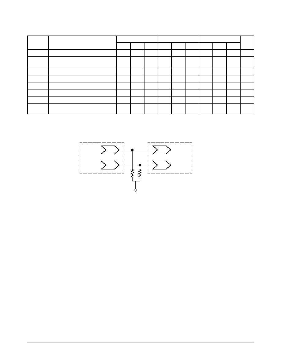
Figure 1. Typical Termination for Output Driver and Device Evaluation
(See Application Note AND8020 ≠ Termination of ECL Logic Devices.)
W
Driver
Device
Receiver
Device
Q
Qb
D
Db
50
W
50
V TT
Resource Reference of Application Notes
AN1404
≠
ECLinPS Circuit Performance at Non≠Standard V
IH
Levels
AN1405
≠
ECL Clock Distribution Techniques
AN1406
≠
Designing with PECL (ECL at +5.0 V)
AN1503
≠
ECLinPS I/O SPICE Modeling Kit
AN1504
≠
Metastability and the ECLinPS Family
AN1560
≠
Low Voltage ECLinPS SPICE Modeling Kit
AN1568
≠
Interfacing Between LVDS and ECL
AN1596
≠
ECLinPS Lite Translator ELT Family SPICE I/O Model Kit
AN1650
≠
Using Wire≠OR Ties in ECLinPS Designs
AN1672
≠
The ECL Translator Guide
AND8001
≠
Odd Number Counters Design
AND8002
≠
Marking and Date Codes
AND8020
≠
Termination of ECL Logic Devices