
©
Semiconductor Components Industries, LLC, 2001
April, 2001 ≠ Rev. 3
1
Publication Order Number:
MC10EP08/D
MC10EP08, MC100EP08
3.3V / 5V ECL 2-Input
Differential XOR/XNOR
The MC10/100EP08 is a differential XOR/XNOR gate. The EP08 is
ideal for applications requiring the fastest AC performance available.
The 100 Series contains temperature compensation.
∑
250 ps Typical Propagation Delay
∑
Maximum Frequency > 3 GHz Typical
∑
PECL Mode Operating Range: V
CC
= 3.0 V to 5.5 V
with V
EE
= 0 V
∑
NECL Mode Operating Range: V
CC
= 0 V
with V
EE
= ≠3.0 V to ≠5.5 V
∑
Open Input Default State
∑
Safety Clamp on Inputs
∑
Q Output Will Default LOW with Inputs Open or at V
EE
http://onsemi.com
Device
Package
Shipping
ORDERING INFORMATION
MC10EP08D
SO≠8
98 Units/Rail
MC10EP08DR2
SO≠8
2500 Tape & Reel
MC100EP08D
SO≠8
98 Units/Rail
MC100EP08DR2
SO≠8
2500 Tape & Reel
MC10EP08DT
TSSOP≠8
100 Units/Rail
MC10EP08DTR2
TSSOP≠8
2500 Tape & Reel
MC100EP08DT
TSSOP≠8
100 Units/Rail
MC100EP08DTR2 TSSOP≠8
2500 Tape & Reel
L = Wafer Lot
Y = Year
W = Work Week
*For additional information, see Application Note
AND8002/D
H = MC10
K = MC100
A = Assembly Location
SO≠8
D SUFFIX
CASE 751
MARKING DIAGRAMS*
TSSOP≠8
DT SUFFIX
CASE 948R
ALYW
KEP08
ALYW
HP08
HEP08
ALYW
ALYW
KP08
1
8
1
8
1
8
1
8
1
8
1
8
MC10EP08, MC100EP08
http://onsemi.com
2
1
2
3
4
5
6
7
8
Q
V
EE
V
CC
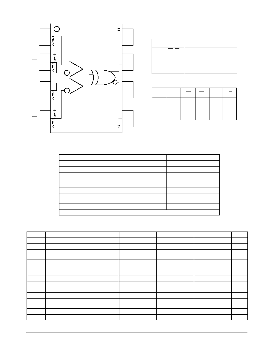
Figure 1. 8≠Lead Pinout (Top View) and Logic Diagram
D0
Q
D1
D1
D0
PIN DESCRIPTION
PIN
D0, D1, D0, D1
Q, Q
ECL Data Outputs
FUNCTION
ECL Data Inputs
D0*
D1*
D0**
D1**
Q
Q
L
L
H
H
L
H
L
H
H
L
H
L
H
L
L
H
H
L
H
H
L
L
L
H
TRUTH TABLE
V
CC
V
EE
Positive Supply
Negative Supply
* Pins will default LOW when left open.
** Pins will default to V
CC
/2 when left open.
ATTRIBUTES
Characteristics
Value
Internal Input Pulldown Resistor
75 k
W
Internal Input Pullup Resistor
37.5 k
W
ESD Protection
Human Body Model
Machine Model
Charged Device Model
> 4 kV
> 200 V
> 2 kV
Moisture Sensitivity, Indefinite Time Out of Drypack (Note 1.)
Level 1
Flammability Rating
Oxygen Index
UL≠94 code V≠0 A 1/8"
28 to 34
Transistor Count
135
Meets or exceeds JEDEC Spec EIA/JESD78 IC Latchup Test
1. For additional information, see Application Note AND8003/D.
MAXIMUM RATINGS
(Note 2.)
Symbol
Parameter
Condition 1
Condition 2
Rating
Units
V
CC
PECL Mode Power Supply
V
EE
= 0 V
6
V
V
EE
NECL Mode Power Supply
V
CC
= 0 V
≠6
V
V
I
PECL Mode Input Voltage
V
EE
= 0 V
V
I
V
CC
6
V
V
I
PECL Mode In ut Voltage
NECL Mode Input Voltage
V
EE
0 V
V
CC
= 0 V
V
I
V
CC
V
I
V
EE
6
≠6
V
V
I
out
Output Current
Continuous
Surge
50
100
mA
mA
TA
Operating Temperature Range
≠40 to +85
∞
C
T
stg
Storage Temperature Range
≠65 to +150
∞
C
JA
Thermal Resistance (Junction to Ambient)
0 LFPM
500 LFPM
8 SOIC
8 SOIC
190
130
∞
C/W
∞
C/W
JC
Thermal Resistance (Junction to Case)
std bd
8 SOIC
41 to 44
∞
C/W
JA
Thermal Resistance (Junction to Ambient)
0 LFPM
500 LFPM
8 TSSOP
8 TSSOP
185
140
∞
C/W
∞
C/W
JC
Thermal Resistance (Junction to Case)
std bd
8 TSSOP
41 to 44
∞
C/W
T
sol
Wave Solder
<2 to 3 sec @ 248
∞
C
265
∞
C
2. Maximum Ratings are those values beyond which device damage may occur.
MC10EP08, MC100EP08
http://onsemi.com
3
10EP DC CHARACTERISTICS, PECL
V
CC
= 3.3 V, V
EE
= 0 V (Note 3.)
≠40
∞
C
25
∞
C
85
∞
C
Symbol
Characteristic
Min
Typ
Max
Min
Typ
Max
Min
Typ
Max
Unit
I
EE
Power Supply Current
20
28
36
20
30
38
20
32
38
mA
V
OH
Output HIGH Voltage (Note 4.)
2165
2290
2415
2230
2355
2480
2290
2415
2540
mV
V
OL
Output LOW Voltage (Note 4.)
1365
1490
1615
1430
1555
1680
1490
1615
1740
mV
V
IH
Input HIGH Voltage (Single Ended)
2090
2415
2155
2480
2215
2540
mV
V
IL
Input LOW Voltage (Single Ended)
1365
1690
1430
1755
1490
1815
mV
V
IHCMR
Input HIGH Voltage Common Mode
Range (Differential) (Note 5.)
2.0
3.3
2.0
3.3
2.0
3.3
V
I
IH
Input HIGH Current
150
150
150
µ
A
I
IL
Input LOW Current
D
D
0.5
≠150
0.5
≠150
0.5
≠150
µ
A
NOTE: EP circuits are designed to meet the DC specifications shown in the above table after thermal equilibrium has been established. The
circuit is in a test socket or mounted on a printed circuit board and transverse airflow greater than 500 lfpm is maintained.
3. Input and output parameters vary 1:1 with V
CC
. V
EE
can vary +0.3 V to ≠2.2 V.
4. All loading with 50 ohms to V
CC
≠2.0 volts.
5. V
IHCMR
min varies 1:1 with V
EE
, V
IHCMR
max varies 1:1 with V
CC
. The V
IHCMR
range is referenced to the most positive side of the differential
input signal.
10EP DC CHARACTERISTICS, PECL
V
CC
= 5.0 V, V
EE
= 0 V (Note 6.)
≠40
∞
C
25
∞
C
85
∞
C
Symbol
Characteristic
Min
Typ
Max
Min
Typ
Max
Min
Typ
Max
Unit
I
EE
Power Supply Current
20
28
36
20
30
38
20
32
38
mA
V
OH
Output HIGH Voltage (Note 7.)
3865
3940
4115
3930
4055
4180
3990
4115
4240
mV
V
OL
Output LOW Voltage (Note 7.)
3065
3190
3315
3130
3255
3380
3190
3315
3440
mV
V
IH
Input HIGH Voltage (Single Ended)
3790
4115
3855
4180
3915
4240
mV
V
IL
Input LOW Voltage (Single Ended)
3065
3390
3130
3455
3190
3515
mV
V
IHCMR
Input HIGH Voltage Common Mode
Range (Differential) (Note 8.)
2.0
5.0
2.0
5.0
2.0
5.0
V
I
IH
Input HIGH Current
150
150
150
µ
A
I
IL
Input LOW Current
D
D
0.5
≠150
0.5
≠150
0.5
≠150
µ
A
NOTE: EP circuits are designed to meet the DC specifications shown in the above table after thermal equilibrium has been established. The
circuit is in a test socket or mounted on a printed circuit board and transverse airflow greater than 500 lfpm is maintained.
6. Input and output parameters vary 1:1 with V
CC
. V
EE
can vary +2.0 V to ≠0.5 V.
7. All loading with 50 ohms to V
CC
≠2.0 volts.
8. V
IHCMR
min varies 1:1 with V
EE
, V
IHCMR
max varies 1:1 with V
CC
. The V
IHCMR
range is referenced to the most positive side of the differential
input signal.
10EP DC CHARACTERISTICS, NECL
V
CC
= 0 V; V
EE
= ≠5.5 V to ≠3.0 V (Note 9.)
≠40
∞
C
25
∞
C
85
∞
C
Symbol
Characteristic
Min
Typ
Max
Min
Typ
Max
Min
Typ
Max
Unit
I
EE
Power Supply Current
20
28
36
20
30
38
20
32
38
mA
V
OH
Output HIGH Voltage (Note 10.)
≠1135
≠1010
≠885
≠1070
≠945
≠820
≠1010
≠885
≠760
mV
V
OL
Output LOW Voltage (Note 10.)
≠1935
≠1810
≠1685
≠1870
≠1745
≠1620
≠1810
≠1685
≠1560
mV
V
IH
Input HIGH Voltage (Single Ended)
≠1210
≠885
≠1145
≠820
≠1085
≠760
mV
V
IL
Input LOW Voltage (Single Ended)
≠1935
≠1610
≠1870
≠1545
≠1810
≠1485
mV
V
IHCMR
Input HIGH Voltage Common Mode
Range (Differential) (Note 11.)
V
EE
+2.0
0.0
V
EE
+2.0
0.0
V
EE
+2.0
0.0
V
I
IH
Input HIGH Current
150
150
150
µ
A
I
IL
Input LOW Current
D
D
0.5
≠150
0.5
≠150
0.5
≠150
µ
A
NOTE: EP circuits are designed to meet the DC specifications shown in the above table after thermal equilibrium has been established. The
circuit is in a test socket or mounted on a printed circuit board and transverse airflow greater than 500 lfpm is maintained.
9. Input and output parameters vary 1:1 with V
CC
.
10. All loading with 50 ohms to V
CC
≠2.0 volts.
11. V
IHCMR
min varies 1:1 with V
EE
, V
IHCMR
max varies 1:1 with V
CC
. The V
IHCMR
range is referenced to the most positive side of the differential
input signal.

MC10EP08, MC100EP08
http://onsemi.com
4
100EP DC CHARACTERISTICS, PECL
V
CC
= 3.3 V, V
EE
= 0 V (Note 12.)
≠40
∞
C
25
∞
C
85
∞
C
Symbol
Characteristic
Min
Typ
Max
Min
Typ
Max
Min
Typ
Max
Unit
I
EE
Power Supply Current
20
28
36
20
30
38
20
32
40
mA
V
OH
Output HIGH Voltage (Note 13.)
2155
2280
2405
2155
2280
2405
2155
2280
2405
mV
V
OL
Output LOW Voltage (Note 13.)
1355
1480
1605
1355
1480
1605
1355
1480
1605
mV
V
IH
Input HIGH Voltage (Single Ended)
2075
2420
2075
2420
2075
2420
mV
V
IL
Input LOW Voltage (Single Ended)
1355
1675
1355
1675
1355
1675
mV
V
IHCMR
Input HIGH Voltage Common Mode
Range (Differential) (Note 14.)
2.0
3.3
2.0
3.3
2.0
3.3
V
I
IH
Input HIGH Current
150
150
150
µ
A
I
IL
Input LOW Current
D
D
0.5
≠150
0.5
≠150
0.5
≠150
µ
A
NOTE: EP circuits are designed to meet the DC specifications shown in the above table after thermal equilibrium has been established. The
circuit is in a test socket or mounted on a printed circuit board and transverse airflow greater than 500 lfpm is maintained.
12. Input and output parameters vary 1:1 with V
CC
. V
EE
can vary +0.3 V to ≠2.2 V.
13. All loading with 50 ohms to V
CC
≠2.0 volts.
14. V
IHCMR
min varies 1:1 with V
EE
, V
IHCMR
max varies 1:1 with V
CC
. The V
IHCMR
range is referenced to the most positive side of the differential
input signal.
100EP DC CHARACTERISTICS, PECL
V
CC
= 5.0 V, V
EE
= 0 V (Note 15.)
≠40
∞
C
25
∞
C
85
∞
C
Symbol
Characteristic
Min
Typ
Max
Min
Typ
Max
Min
Typ
Max
Unit
I
EE
Power Supply Current
20
28
36
20
30
38
20
32
40
mA
V
OH
Output HIGH Voltage (Note 16.)
3855
3980
4105
3855
3980
4105
3855
3980
4105
mV
V
OL
Output LOW Voltage (Note 16.)
3055
3180
3305
3055
3180
3305
3055
3180
3305
mV
V
IH
Input HIGH Voltage (Single Ended)
3775
4120
3775
4120
3775
4120
mV
V
IL
Input LOW Voltage (Single Ended)
3055
3375
3055
3375
3055
3375
mV
V
IHCMR
Input HIGH Voltage Common Mode
Range (Differential) (Note 17.)
2.0
5.0
2.0
5.0
2.0
5.0
V
I
IH
Input HIGH Current
150
150
150
µ
A
I
IL
Input LOW Current
D
D
0.5
≠150
0.5
≠150
0.5
≠150
µ
A
NOTE: EP circuits are designed to meet the DC specifications shown in the above table after thermal equilibrium has been established. The
circuit is in a test socket or mounted on a printed circuit board and transverse airflow greater than 500 lfpm is maintained.
15. Input and output parameters vary 1:1 with V
CC
. V
EE
can vary +2.0 V to ≠0.5 V.
16. All loading with 50 ohms to V
CC
≠2.0 volts.
17. V
IHCMR
min varies 1:1 with V
EE
, V
IHCMR
max varies 1:1 with V
CC
. The V
IHCMR
range is referenced to the most positive side of the differential
input signal.
100EP DC CHARACTERISTICS, NECL
V
CC
= 0 V; V
EE
= ≠5.5 V to ≠3.0 V (Note 18.)
≠40
∞
C
25
∞
C
85
∞
C
Symbol
Characteristic
Min
Typ
Max
Min
Typ
Max
Min
Typ
Max
Unit
I
EE
Power Supply Current
20
28
36
20
30
38
20
32
40
mA
V
OH
Output HIGH Voltage (Note 19.)
≠1145
≠1020
≠895
≠1145
≠1020
≠895
≠1145
≠1020
≠895
mV
V
OL
Output LOW Voltage (Note 19.)
≠1945
≠1820
≠1695
≠1945
≠1820
≠1695
≠1945
≠1820
≠1695
mV
V
IH
Input HIGH Voltage (Single Ended)
≠1225
≠880
≠1225
≠880
≠1225
≠880
mV
V
IL
Input LOW Voltage (Single Ended)
≠1945
≠1625
≠1945
≠1625
≠1945
≠1625
mV
V
IHCMR
Input HIGH Voltage Common Mode
Range (Differential) (Note 20.)
V
EE
+2.0
0.0
V
EE
+2.0
0.0
V
EE
+2.0
0.0
V
I
IH
Input HIGH Current
150
150
150
µ
A
I
IL
Input LOW Current
D
D
0.5
≠150
0.5
≠150
0.5
≠150
µ
A
NOTE: EP circuits are designed to meet the DC specifications shown in the above table after thermal equilibrium has been established. The
circuit is in a test socket or mounted on a printed circuit board and transverse airflow greater than 500 lfpm is maintained.
18. Input and output parameters vary 1:1 with V
CC
.
19. All loading with 50 ohms to V
CC
≠2.0 volts.
20. V
IHCMR
min varies 1:1 with V
EE
, V
IHCMR
max varies 1:1 with V
CC
. The V
IHCMR
range is referenced to the most positive side of the differential
input signal.
MC10EP08, MC100EP08
http://onsemi.com
5
AC CHARACTERISTICS
V
CC
= 0 V; V
EE
= ≠3.0 V to ≠5.5 V or V
CC
= 3.0 V to 5.5 V; V
EE
= 0 V (Note 21.)
≠40
∞
C
25
∞
C
85
∞
C
Symbol
Characteristic
Min
Typ
Max
Min
Typ
Max
Min
Typ
Max
Unit
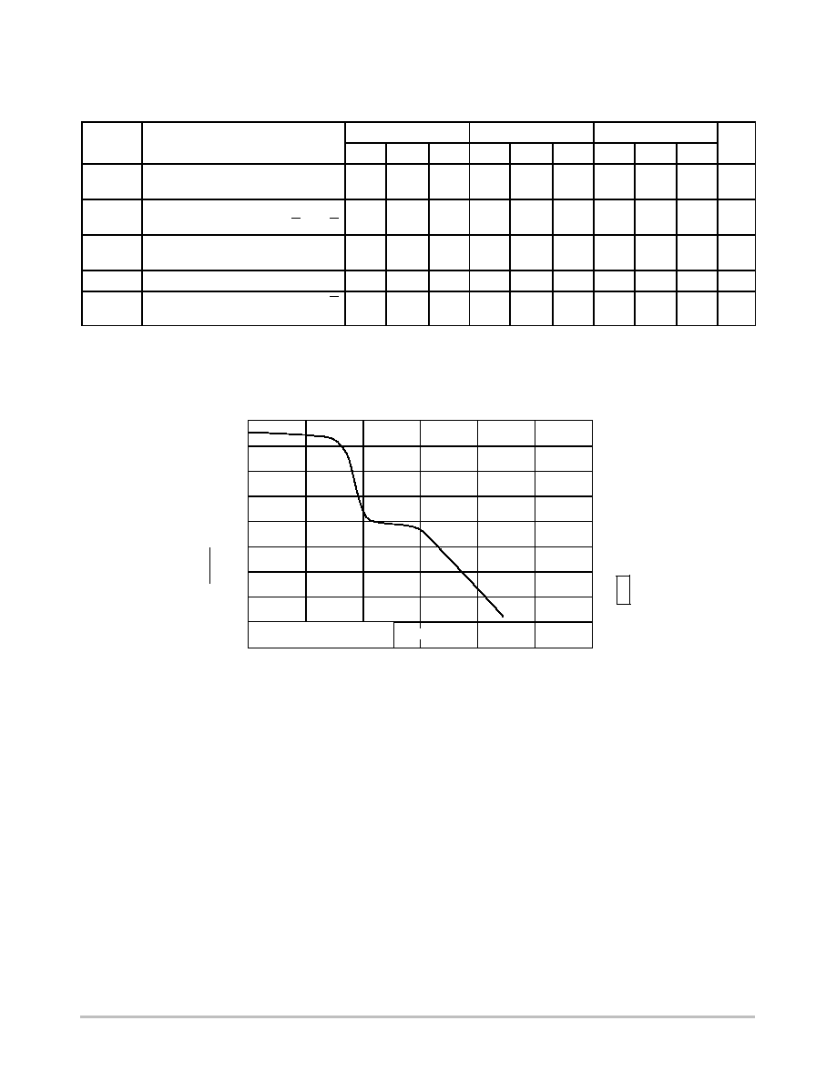
f
max
Maximum Frequency
(See Figure 2. F
max
/JITTER)
> 3
> 3
> 3
GHz
t
PLH
,
t
PHL
Propagation Delay to
Output Differential
D, D to Q, Q
170
220
280
180
250
300
200
270
320
ps
t
JITTER
Cycle≠to≠Cycle Jitter
(See Figure 2. F
max
/JITTER)
0.2
< 1
0.2
< 1
0.2
< 1
ps
V
PP
Input Voltage Swing (Differential)
150
800
1200
150
800
1200
150
800
1200
mV
t
r
t
f
Output Rise/Fall Times
Q, Q
(20% ≠ 80%)
70
120
170
80
130
180
100
150
200
ps
21. Measured using a 750 mV source, 50% duty cycle clock source. All loading with 50 ohms to V
CC
≠2.0 V.
0
100
200
300
400
500
600
700
800
900
0
1000
2000
3000
4000
5000
6000
Figure 2. F
max
/Jitter
FREQUENCY (MHz)
1
2
3
4
5
6
7
8
(JITTER)
……………………
……………………
9
V
OUTpp
(mV)
JITTER
OUT
ps (RMS)
……
……