©
Semiconductor Components Industries, LLC, 2005
February, 2005 - Rev. 4
1
Publication Order Number:
MC14001B/D
MC14001B Series
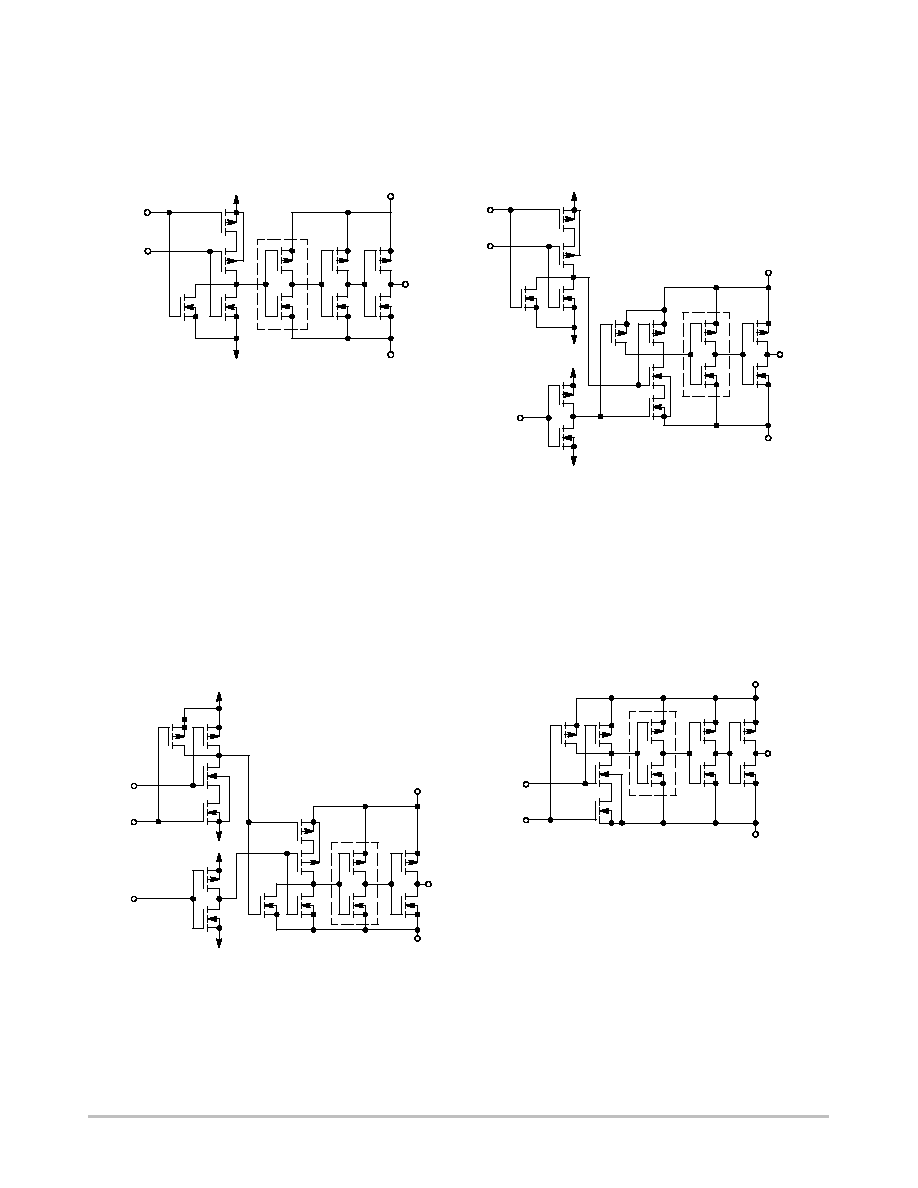
B-Suffix Series CMOS Gates
MC14001B, MC14011B, MC14023B,
MC14025B, MC14071B, MC14073B,
MC14081B, MC14082B
The B Series logic gates are constructed with P and N channel
enhancement mode devices in a single monolithic structure
(Complementary MOS). Their primary use is where low power
dissipation and/or high noise immunity is desired.
Features
∑
Supply Voltage Range = 3.0 Vdc to 18 Vdc
∑
All Outputs Buffered
∑
Capable of Driving Two Low-power TTL Loads or One Low-power
Schottky TTL Load Over the Rated Temperature Range.
∑
Double Diode Protection on All Inputs Except: Triple Diode
Protection on MC14011B and MC14081B
∑
Pin-for-Pin Replacements for Corresponding CD4000 Series
B Suffix Devices
∑
Pb-Free Packages are Available*
MAXIMUM RATINGS
(Voltages Referenced to V
SS
)
Symbol
Parameter
Value
Unit
V
DD
DC Supply Voltage Range
- 0.5 to +18.0
V
V
in
, V
out
Input or Output Voltage Range
(DC or Transient)
- 0.5 to V
DD
+ 0.5
V
I
in
, I
out
Input or Output Current
(DC or Transient) per Pin
±
10
mA
P
D
Power Dissipation, per Package
(Note 1)
500
mW
T
A
Ambient Temperature Range
- 55 to +125
∞
C
T
stg
Storage Temperature Range
- 65 to +150
∞
C
T
L
Lead Temperature
(8-Second Soldering)
260
∞
C
Maximum ratings are those values beyond which device damage can occur.
Maximum ratings applied to the device are individual stress limit values (not
normal operating conditions) and are not valid simultaneously. If these limits are
exceeded, device functional operation is not implied, damage may occur and
reliability may be affected.
1. Temperature Derating:
Plastic "P and D/DW" Packages: ≠ 7.0 mW/
_
C From 65
_
C To 125
_
C
This device contains protection circuitry to guard against damage due to high
static voltages or electric fields. However, precautions must be taken to avoid
applications of any voltage higher than maximum rated voltages to this
high-impedance circuit. For proper operation, V
in
and V
out
should be constrained
to the range V
SS
v
(V
in
or V
out
)
v
V
DD
.
Unused inputs must always be tied to an appropriate logic voltage level
(e.g., either V
SS
or V
DD
). Unused outputs must be left open.
*For additional information on our Pb-Free strategy and soldering details, please
download the ON Semiconductor Soldering and Mounting Techniques
Reference Manual, SOLDERRM/D.
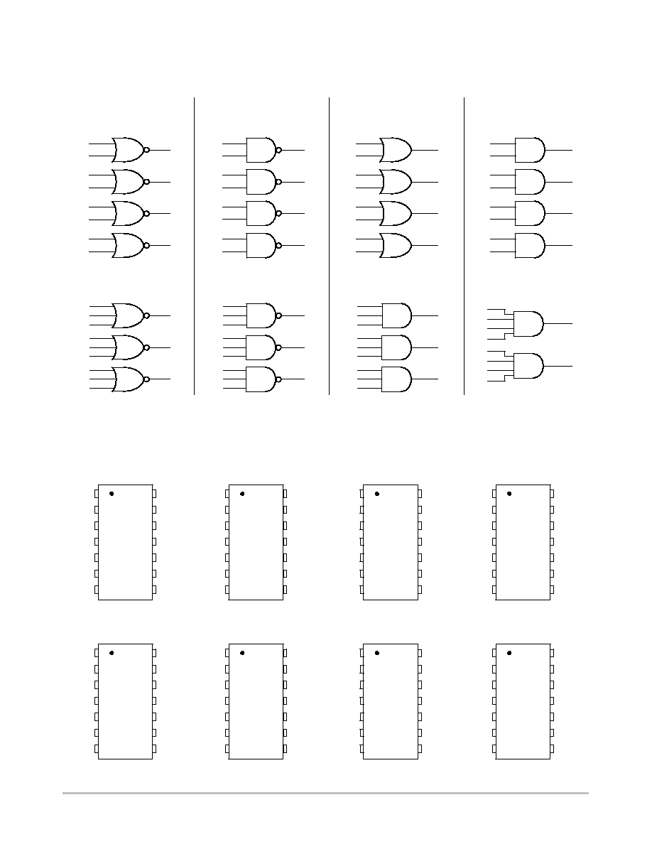
Device
Description
DEVICE INFORMATION
MC14001B
Quad 2-Input NOR Gate
MC14011B
Quad 2-Input NAND Gate
MC14023B
Triple 3-Input NAND Gate
MC14025B
Triple 3-Input NOR Gate
MC14071B
Quad 2-Input OR Gate
MARKING
DIAGRAMS
1
14
PDIP-14
P SUFFIX
CASE 646
MC140xxBCP
AWLYYWW
SOIC-14
D SUFFIX
CASE 751A
TSSOP-14
DT SUFFIX
CASE 948G
1
14
140xxB
AWLYWW
14
0xxB
ALYW
1
14
xx
= Specific Device Code
A
= Assembly Location
WL, L
= Wafer Lot
YY, Y
= Year
WW, W
= Work Week
SOEIAJ-14
F SUFFIX
CASE 965
1
14
MC140xxB
AWLYWW
MC14073B
Triple 3-Input AND Gate
MC14081B
Quad 2-Input AND Gate
MC14082B
Dual 4-Input AND Gate
See detailed ordering and shipping information in the package
dimensions section on page 8 of this data sheet.
ORDERING INFORMATION
http://onsemi.com

MC14001B Series
http://onsemi.com
3
ŒŒŒŒŒŒŒŒŒŒŒŒŒŒŒŒŒŒŒŒŒŒŒŒŒŒŒŒŒŒŒŒŒ
ŒŒŒŒŒŒŒŒŒŒŒŒŒŒŒŒŒŒŒŒŒŒŒŒŒŒŒŒŒŒŒŒŒ
ELECTRICAL CHARACTERISTICS
(Voltages Referenced to V
SS
)
ŒŒŒŒŒŒŒŒŒŒ
ŒŒŒŒŒŒŒŒŒŒ
ŒŒŒŒ
ŒŒŒŒ
ŒŒŒ
ŒŒŒ
V
DD
ŒŒŒŒŒ
ŒŒŒŒŒ
- 55
_
C
ŒŒŒŒŒŒŒŒŒ
ŒŒŒŒŒŒŒŒŒ
25
_
C
ŒŒŒŒŒ
ŒŒŒŒŒ
125
_
C
ŒŒŒ
ŒŒŒ
ŒŒŒŒŒŒŒŒŒŒ
ŒŒŒŒŒŒŒŒŒŒ
Characteristic
ŒŒŒŒ
ŒŒŒŒ
Symbol
ŒŒŒ
ŒŒŒ
V
DD
Vdc
ŒŒŒ
ŒŒŒ
Min
ŒŒŒ
ŒŒŒ
Max
ŒŒŒŒ
ŒŒŒŒ
Min
ŒŒŒ
ŒŒŒ
Typ
(2)
ŒŒŒŒ
ŒŒŒŒ
Max
ŒŒŒ
ŒŒŒ
Min
ŒŒŒ
ŒŒŒ
Max
ŒŒŒ
ŒŒŒ
Unit
ŒŒŒŒŒŒŒŒŒŒ
Œ
ŒŒŒŒŒŒŒŒ
Œ
ŒŒŒŒŒŒŒŒŒŒ
Output Voltage
"0" Level
V
in
= V
DD
or 0
ŒŒŒŒ
Œ
ŒŒ
Œ
ŒŒŒŒ
V
OL
ŒŒŒ
Œ
Œ
Œ
ŒŒŒ
5.0
10
15
ŒŒŒ
Œ
Œ
Œ
ŒŒŒ
-
-
-
ŒŒŒ
Œ
Œ
Œ
ŒŒŒ
0.05
0.05
0.05
ŒŒŒŒ
Œ
ŒŒ
Œ
ŒŒŒŒ
-
-
-
ŒŒŒ
Œ
Œ
Œ
ŒŒŒ
0
0
0
ŒŒŒŒ
Œ
ŒŒ
Œ
ŒŒŒŒ
0.05
0.05
0.05
ŒŒŒ
Œ
Œ
Œ
ŒŒŒ
-
-
-
ŒŒŒ
Œ
Œ
Œ
ŒŒŒ
0.05
0.05
0.05
ŒŒŒ
Œ
Œ
Œ
ŒŒŒ
Vdc
ŒŒŒŒŒŒŒŒŒŒ
Œ
ŒŒŒŒŒŒŒŒ
Œ
ŒŒŒŒŒŒŒŒŒŒ
"1" Level
V
in
= 0 or V
DD
ŒŒŒŒ
Œ
ŒŒ
Œ
ŒŒŒŒ
V
OH
ŒŒŒ
Œ
Œ
Œ
ŒŒŒ
5.0
10
15
ŒŒŒ
Œ
Œ
Œ
ŒŒŒ
4.95
9.95
14.95
ŒŒŒ
Œ
Œ
Œ
ŒŒŒ
-
-
-
ŒŒŒŒ
Œ
ŒŒ
Œ
ŒŒŒŒ
4.95
9.95
14.95
ŒŒŒ
Œ
Œ
Œ
ŒŒŒ
5.0
10
15
ŒŒŒŒ
Œ
ŒŒ
Œ
ŒŒŒŒ
-
-
-
ŒŒŒ
Œ
Œ
Œ
ŒŒŒ
4.95
9.95
14.95
ŒŒŒ
Œ
Œ
Œ
ŒŒŒ
-
-
-
ŒŒŒ
Œ
Œ
Œ
ŒŒŒ
Vdc
ŒŒŒŒŒŒŒŒŒŒ
Œ
ŒŒŒŒŒŒŒŒ
Œ
Œ
ŒŒŒŒŒŒŒŒ
Œ
ŒŒŒŒŒŒŒŒŒŒ
Input Voltage
"0" Level
(V
O
= 4.5 or 0.5 Vdc)
(V
O
= 9.0 or 1.0 Vdc)
(V
O
= 13.5 or 1.5 Vdc)
ŒŒŒŒ
Œ
ŒŒ
Œ
Œ
ŒŒ
Œ
ŒŒŒŒ
V
IL
ŒŒŒ
Œ
Œ
Œ
Œ
Œ
Œ
ŒŒŒ
5.0
10
15
ŒŒŒ
Œ
Œ
Œ
Œ
Œ
Œ
ŒŒŒ
-
-
-
ŒŒŒ
Œ
Œ
Œ
Œ
Œ
Œ
ŒŒŒ
1.5
3.0
4.0
ŒŒŒŒ
Œ
ŒŒ
Œ
Œ
ŒŒ
Œ
ŒŒŒŒ
-
-
-
ŒŒŒ
Œ
Œ
Œ
Œ
Œ
Œ
ŒŒŒ
2.25
4.50
6.75
ŒŒŒŒ
Œ
ŒŒ
Œ
Œ
ŒŒ
Œ
ŒŒŒŒ
1.5
3.0
4.0
ŒŒŒ
Œ
Œ
Œ
Œ
Œ
Œ
ŒŒŒ
-
-
-
ŒŒŒ
Œ
Œ
Œ
Œ
Œ
Œ
ŒŒŒ
1.5
3.0
4.0
ŒŒŒ
Œ
Œ
Œ
Œ
Œ
Œ
ŒŒŒ
Vdc
ŒŒŒŒŒŒŒŒŒŒ
Œ
ŒŒŒŒŒŒŒŒ
Œ
Œ
ŒŒŒŒŒŒŒŒ
Œ
ŒŒŒŒŒŒŒŒŒŒ
"1" Level
(V
O
= 0.5 or 4.5 Vdc)
(V
O
= 1.0 or 9.0 Vdc)
(V
O
= 1.5 or 13.5 Vdc)
ŒŒŒŒ
Œ
ŒŒ
Œ
Œ
ŒŒ
Œ
ŒŒŒŒ
V
IH
ŒŒŒ
Œ
Œ
Œ
Œ
Œ
Œ
ŒŒŒ
5.0
10
15
ŒŒŒ
Œ
Œ
Œ
Œ
Œ
Œ
ŒŒŒ
3.5
7.0
11
ŒŒŒ
Œ
Œ
Œ
Œ
Œ
Œ
ŒŒŒ
-
-
-
ŒŒŒŒ
Œ
ŒŒ
Œ
Œ
ŒŒ
Œ
ŒŒŒŒ
3.5
7.0
11
ŒŒŒ
Œ
Œ
Œ
Œ
Œ
Œ
ŒŒŒ
2.75
5.50
8.25
ŒŒŒŒ
Œ
ŒŒ
Œ
Œ
ŒŒ
Œ
ŒŒŒŒ
-
-
-
ŒŒŒ
Œ
Œ
Œ
Œ
Œ
Œ
ŒŒŒ
3.5
7.0
11
ŒŒŒ
Œ
Œ
Œ
Œ
Œ
Œ
ŒŒŒ
-
-
-
ŒŒŒ
Œ
Œ
Œ
Œ
Œ
Œ
ŒŒŒ
Vdc
ŒŒŒŒŒŒŒŒŒŒ
Œ
ŒŒŒŒŒŒŒŒ
Œ
Œ
ŒŒŒŒŒŒŒŒ
Œ
Œ
ŒŒŒŒŒŒŒŒ
Œ
ŒŒŒŒŒŒŒŒŒŒ
Output Drive Current
(V
OH
= 2.5 Vdc)
Source
(V
OH
= 4.6 Vdc)
(V
OH
= 9.5 Vdc)
(V
OH
= 13.5 Vdc)
ŒŒŒŒ
Œ
ŒŒ
Œ
Œ
ŒŒ
Œ
Œ
ŒŒ
Œ
ŒŒŒŒ
I
OH
ŒŒŒ
Œ
Œ
Œ
Œ
Œ
Œ
Œ
Œ
Œ
ŒŒŒ
5.0
5.0
10
15
ŒŒŒ
Œ
Œ
Œ
Œ
Œ
Œ
Œ
Œ
Œ
ŒŒŒ
≠ 3.0
≠ 0.64
≠ 1.6
≠ 4.2
ŒŒŒ
Œ
Œ
Œ
Œ
Œ
Œ
Œ
Œ
Œ
ŒŒŒ
-
-
-
-
ŒŒŒŒ
Œ
ŒŒ
Œ
Œ
ŒŒ
Œ
Œ
ŒŒ
Œ
ŒŒŒŒ
≠ 2.4
≠ 0.51
≠ 1.3
≠ 3.4
ŒŒŒ
Œ
Œ
Œ
Œ
Œ
Œ
Œ
Œ
Œ
ŒŒŒ
≠ 4.2
≠ 0.88
≠ 2.25
≠ 8.8
ŒŒŒŒ
Œ
ŒŒ
Œ
Œ
ŒŒ
Œ
Œ
ŒŒ
Œ
ŒŒŒŒ
-
-
-
-
ŒŒŒ
Œ
Œ
Œ
Œ
Œ
Œ
Œ
Œ
Œ
ŒŒŒ
≠ 1.7
≠ 0.36
≠ 0.9
≠ 2.4
ŒŒŒ
Œ
Œ
Œ
Œ
Œ
Œ
Œ
Œ
Œ
ŒŒŒ
-
-
-
-
ŒŒŒ
Œ
Œ
Œ
Œ
Œ
Œ
Œ
Œ
Œ
ŒŒŒ
mAdc
ŒŒŒŒŒŒŒŒŒŒ
Œ
ŒŒŒŒŒŒŒŒ
Œ
ŒŒŒŒŒŒŒŒŒŒ
(V
OL
= 0.4 Vdc)
Sink
(V
OL
= 0.5 Vdc)
(V
OL
= 1.5 Vdc)
ŒŒŒŒ
Œ
ŒŒ
Œ
ŒŒŒŒ
I
OL
ŒŒŒ
Œ
Œ
Œ
ŒŒŒ
5.0
10
15
ŒŒŒ
Œ
Œ
Œ
ŒŒŒ
0.64
1.6
4.2
ŒŒŒ
Œ
Œ
Œ
ŒŒŒ
-
-
-
ŒŒŒŒ
Œ
ŒŒ
Œ
ŒŒŒŒ
0.51
1.3
3.4
ŒŒŒ
Œ
Œ
Œ
ŒŒŒ
0.88
2.25
8.8
ŒŒŒŒ
Œ
ŒŒ
Œ
ŒŒŒŒ
-
-
-
ŒŒŒ
Œ
Œ
Œ
ŒŒŒ
0.36
0.9
2.4
ŒŒŒ
Œ
Œ
Œ
ŒŒŒ
-
-
-
ŒŒŒ
Œ
Œ
Œ
ŒŒŒ
mAdc
ŒŒŒŒŒŒŒŒŒŒ
ŒŒŒŒŒŒŒŒŒŒ
Input Current
ŒŒŒŒ
ŒŒŒŒ
I
in
ŒŒŒ
ŒŒŒ
15
ŒŒŒ
ŒŒŒ
-
ŒŒŒ
ŒŒŒ
±
0.1
ŒŒŒŒ
ŒŒŒŒ
-
ŒŒŒ
ŒŒŒ
±
0.00001
ŒŒŒŒ
ŒŒŒŒ
±
0.1
ŒŒŒ
ŒŒŒ
-
ŒŒŒ
ŒŒŒ
±
1.0
ŒŒŒ
ŒŒŒ
m
Adc
ŒŒŒŒŒŒŒŒŒŒ
Œ
ŒŒŒŒŒŒŒŒ
Œ
ŒŒŒŒŒŒŒŒŒŒ
Input Capacitance
(V
in
= 0)
ŒŒŒŒ
Œ
ŒŒ
Œ
ŒŒŒŒ
C
in
ŒŒŒ
Œ
Œ
Œ
ŒŒŒ
-
ŒŒŒ
Œ
Œ
Œ
ŒŒŒ
-
ŒŒŒ
Œ
Œ
Œ
ŒŒŒ
-
ŒŒŒŒ
Œ
ŒŒ
Œ
ŒŒŒŒ
-
ŒŒŒ
Œ
Œ
Œ
ŒŒŒ
5.0
ŒŒŒŒ
Œ
ŒŒ
Œ
ŒŒŒŒ
7.5
ŒŒŒ
Œ
Œ
Œ
ŒŒŒ
-
ŒŒŒ
Œ
Œ
Œ
ŒŒŒ
-
ŒŒŒ
Œ
Œ
Œ
ŒŒŒ
pF
ŒŒŒŒŒŒŒŒŒŒ
Œ
ŒŒŒŒŒŒŒŒ
Œ
ŒŒŒŒŒŒŒŒŒŒ
Quiescent Current
(Per Package)
ŒŒŒŒ
Œ
ŒŒ
Œ
ŒŒŒŒ
I
DD
ŒŒŒ
Œ
Œ
Œ
ŒŒŒ
5.0
10
15
ŒŒŒ
Œ
Œ
Œ
ŒŒŒ
-
-
-
ŒŒŒ
Œ
Œ
Œ
ŒŒŒ
0.25
0.5
1.0
ŒŒŒŒ
Œ
ŒŒ
Œ
ŒŒŒŒ
-
-
-
ŒŒŒ
Œ
Œ
Œ
ŒŒŒ
0.0005
0.0010
0.0015
ŒŒŒŒ
Œ
ŒŒ
Œ
ŒŒŒŒ
0.25
0.5
1.0
ŒŒŒ
Œ
Œ
Œ
ŒŒŒ
-
-
-
ŒŒŒ
Œ
Œ
Œ
ŒŒŒ
7.5
15
30
ŒŒŒ
Œ
Œ
Œ
ŒŒŒ
m
Adc
ŒŒŒŒŒŒŒŒŒŒ
Œ
ŒŒŒŒŒŒŒŒ
Œ
Œ
ŒŒŒŒŒŒŒŒ
Œ
ŒŒŒŒŒŒŒŒŒŒ
Total Supply Current
(3) (4)
(Dynamic plus Quiescent,
Per Gate, C
L
= 50 pF)
ŒŒŒŒ
Œ
ŒŒ
Œ
Œ
ŒŒ
Œ
ŒŒŒŒ
I
T
ŒŒŒ
Œ
Œ
Œ
Œ
Œ
Œ
ŒŒŒ
5.0
10
15
ŒŒŒŒŒŒŒŒŒŒŒŒŒŒŒŒŒ
Œ
ŒŒŒŒŒŒŒŒŒŒŒŒŒŒŒ
Œ
Œ
ŒŒŒŒŒŒŒŒŒŒŒŒŒŒŒ
Œ
ŒŒŒŒŒŒŒŒŒŒŒŒŒŒŒŒŒ
I
T
= (0.3
m
A/kHz) f + I
DD
/N
I
T
= (0.6
m
A/kHz) f + I
DD
/N
I
T
= (0.9
m
A/kHz) f + I
DD
/N
ŒŒŒ
Œ
Œ
Œ
Œ
Œ
Œ
ŒŒŒ
m
Adc
2. Data labelled "Typ" is not to be used for design purposes but is intended as an indication of the IC's potential performance.
3. The formulas given are for the typical characteristics only at 25
_
C.
4. To calculate total supply current at loads other than 50 pF:
I
T
(C
L
) = I
T
(50 pF) + (C
L
- 50) Vfk
where: I
T
is in
m
A (per package), C
L
in pF, V = (V
DD
- V
SS
) in volts, f in kHz is input frequency, and k = 0.001 x the number of exercised gates
per package.

MC14001B Series
http://onsemi.com
4
B-SERIES GATE SWITCHING TIMES
ŒŒŒŒŒŒŒŒŒŒŒŒŒŒŒŒŒŒŒŒŒŒŒŒŒŒŒŒŒŒŒŒŒ
SWITCHING CHARACTERISTICS
(5)
(C
L
= 50 pF, T
A
= 25
_
C)
ŒŒŒŒŒŒŒŒŒŒŒŒŒŒŒ
Œ
ŒŒŒŒŒŒŒŒŒŒŒŒŒ
Œ
ŒŒŒŒŒŒŒŒŒŒŒŒŒŒŒ
Characteristic
ŒŒŒŒŒ
Œ
ŒŒŒ
Œ
ŒŒŒŒŒ
Symbol
ŒŒŒŒ
Œ
ŒŒ
Œ
ŒŒŒŒ
V
DD
Vdc
ŒŒŒŒ
Œ
ŒŒ
Œ
ŒŒŒŒ
Min
ŒŒŒŒ
Œ
ŒŒ
Œ
ŒŒŒŒ
Typ
(6)
ŒŒŒŒ
Œ
ŒŒ
Œ
ŒŒŒŒ
Max
ŒŒŒ
Œ
Œ
Œ
ŒŒŒ
Unit
ŒŒŒŒŒŒŒŒŒŒŒŒŒŒŒ
Œ
ŒŒŒŒŒŒŒŒŒŒŒŒŒ
Œ
Œ
ŒŒŒŒŒŒŒŒŒŒŒŒŒ
Œ
ŒŒŒŒŒŒŒŒŒŒŒŒŒŒŒ
Output Rise Time, All B-Series Gates
t
TLH
= (1.35 ns/pF) C
L
+ 33 ns
t
TLH
= (0.60 ns/pF) C
L
+ 20 ns
t
TLH
= (0.40 ns/PF) C
L
+ 20 ns
ŒŒŒŒŒ
Œ
ŒŒŒ
Œ
Œ
ŒŒŒ
Œ
ŒŒŒŒŒ
t
TLH
ŒŒŒŒ
Œ
ŒŒ
Œ
Œ
ŒŒ
Œ
ŒŒŒŒ
5.0
10
15
ŒŒŒŒ
Œ
ŒŒ
Œ
Œ
ŒŒ
Œ
ŒŒŒŒ
-
-
-
ŒŒŒŒ
Œ
ŒŒ
Œ
Œ
ŒŒ
Œ
ŒŒŒŒ
100
50
40
ŒŒŒŒ
Œ
ŒŒ
Œ
Œ
ŒŒ
Œ
ŒŒŒŒ
200
100
80
ŒŒŒ
Œ
Œ
Œ
Œ
Œ
Œ
ŒŒŒ
ns
ŒŒŒŒŒŒŒŒŒŒŒŒŒŒŒ
Œ
ŒŒŒŒŒŒŒŒŒŒŒŒŒ
Œ
Œ
ŒŒŒŒŒŒŒŒŒŒŒŒŒ
Œ
ŒŒŒŒŒŒŒŒŒŒŒŒŒŒŒ
Output Fall Time, All B-Series Gates
t
THL
= (1.35 ns/pF) C
L
+ 33 ns
t
THL
= (0.60 ns/pF) C
L
+ 20 ns
t
THL
= (0.40 ns/pF) C
L
+ 20 ns
ŒŒŒŒŒ
Œ
ŒŒŒ
Œ
Œ
ŒŒŒ
Œ
ŒŒŒŒŒ
t
THL
ŒŒŒŒ
Œ
ŒŒ
Œ
Œ
ŒŒ
Œ
ŒŒŒŒ
5.0
10
15
ŒŒŒŒ
Œ
ŒŒ
Œ
Œ
ŒŒ
Œ
ŒŒŒŒ
-
-
-
ŒŒŒŒ
Œ
ŒŒ
Œ
Œ
ŒŒ
Œ
ŒŒŒŒ
100
50
40
ŒŒŒŒ
Œ
ŒŒ
Œ
Œ
ŒŒ
Œ
ŒŒŒŒ
200
100
80
ŒŒŒ
Œ
Œ
Œ
Œ
Œ
Œ
ŒŒŒ
ns
ŒŒŒŒŒŒŒŒŒŒŒŒŒŒŒ
Œ
ŒŒŒŒŒŒŒŒŒŒŒŒŒ
Œ
Œ
ŒŒŒŒŒŒŒŒŒŒŒŒŒ
Œ
Œ
ŒŒŒŒŒŒŒŒŒŒŒŒŒ
Œ
Œ
ŒŒŒŒŒŒŒŒŒŒŒŒŒ
Œ
Œ
ŒŒŒŒŒŒŒŒŒŒŒŒŒ
Œ
Œ
ŒŒŒŒŒŒŒŒŒŒŒŒŒ
Œ
Œ
ŒŒŒŒŒŒŒŒŒŒŒŒŒ
Œ
Œ
ŒŒŒŒŒŒŒŒŒŒŒŒŒ
Œ
ŒŒŒŒŒŒŒŒŒŒŒŒŒŒŒ
Propagation Delay Time
MC14001B, MC14011B only
t
PLH
, t
PHL
= (0.90 ns/pF) C
L
+ 80 ns
t
PLH
, t
PHL
= (0.36 ns/pF) C
L
+ 32 ns
t
PLH
, t
PHL
= (0.26 ns/pF) C
L
+ 27 ns
All Other 2, 3, and 4 Input Gates
t
PLH
, t
PHL
= (0.90 ns/pF) C
L
+ 115 ns
t
PLH
, t
PHL
= (0.36 ns/pF) C
L
+ 47 ns
t
PLH
, t
PHL
= (0.26 ns/pF) C
L
+ 37 ns
8-Input Gates (MC14068B, MC14078B)
t
PLH
, t
PHL
= (0.90 ns/pF) C
L
+ 155 ns
t
PLH
, t
PHL
= (0.36 ns/pF) C
L
+ 62 ns
t
PLH
, t
PHL
= (0.26 ns/pF) C
L
+ 47 ns
ŒŒŒŒŒ
Œ
ŒŒŒ
Œ
Œ
ŒŒŒ
Œ
Œ
ŒŒŒ
Œ
Œ
ŒŒŒ
Œ
Œ
ŒŒŒ
Œ
Œ
ŒŒŒ
Œ
Œ
ŒŒŒ
Œ
Œ
ŒŒŒ
Œ
ŒŒŒŒŒ
t
PLH
, t
PHL
ŒŒŒŒ
Œ
ŒŒ
Œ
Œ
ŒŒ
Œ
Œ
ŒŒ
Œ
Œ
ŒŒ
Œ
Œ
ŒŒ
Œ
Œ
ŒŒ
Œ
Œ
ŒŒ
Œ
Œ
ŒŒ
Œ
ŒŒŒŒ
5.0
10
15
5.0
10
15
5.0
10
15
ŒŒŒŒ
Œ
ŒŒ
Œ
Œ
ŒŒ
Œ
Œ
ŒŒ
Œ
Œ
ŒŒ
Œ
Œ
ŒŒ
Œ
Œ
ŒŒ
Œ
Œ
ŒŒ
Œ
Œ
ŒŒ
Œ
ŒŒŒŒ
-
-
-
-
-
-
-
-
-
ŒŒŒŒ
Œ
ŒŒ
Œ
Œ
ŒŒ
Œ
Œ
ŒŒ
Œ
Œ
ŒŒ
Œ
Œ
ŒŒ
Œ
Œ
ŒŒ
Œ
Œ
ŒŒ
Œ
Œ
ŒŒ
Œ
ŒŒŒŒ
125
50
40
160
65
50
200
80
60
ŒŒŒŒ
Œ
ŒŒ
Œ
Œ
ŒŒ
Œ
Œ
ŒŒ
Œ
Œ
ŒŒ
Œ
Œ
ŒŒ
Œ
Œ
ŒŒ
Œ
Œ
ŒŒ
Œ
Œ
ŒŒ
Œ
ŒŒŒŒ
250
100
80
300
130
100
350
150
110
ŒŒŒ
Œ
Œ
Œ
Œ
Œ
Œ
Œ
Œ
Œ
Œ
Œ
Œ
Œ
Œ
Œ
Œ
Œ
Œ
Œ
Œ
Œ
Œ
Œ
Œ
ŒŒŒ
ns
5. The formulas given are for the typical characteristics only at 25
_
C.
6. Data labelled "Typ" is not to be used for design purposes but is intended as an indication of the IC's potential performance.
V
DD
14
C
L
V
SS
7
PULSE
GENERATOR
INPUT
OUTPUT
90%
50%
10%
10%
50%
90%
20 ns
20 ns
t
PHL
t
PLH
t
TLH
t
THL
V
OL
V
OH
0 V
V
DD
INPUT
OUTPUT
INVERTING
*All unused inputs of AND, NAND gates must be connected to V
DD
.
All unused inputs of OR, NOR gates must be connected to V
SS
.
90%
50%
10%
V
OL
V
OH
OUTPUT
NON-INVERTING
t
THL
t
TLH
t
PLH
t
PHL
*
Figure 1. Switching Time Test Circuit and Waveforms