─εΩ≤∞σφ≥α÷Φ Φ ε∩Φ±αφΦ www.docs.chipfind.ru
⌐
Semiconductor Components Industries, LLC, 2000
March, 2000 ¡ Rev. 3
1
Publication Order Number:
MC14094B/D
MC14094B
8-Stage Shift/Store Register
with Three-State Outputs
The MC14094B combines an 8¡stage shift register with a data latch
for each stage and a three¡state output from each latch.
Data is shifted on the positive clock transition and is shifted from the
seventh stage to two serial outputs. The Q
S
output data is for use in
high¡speed cascaded systems. The Q
S
output data is shifted on the
following negative clock transition for use in low¡speed cascaded
systems.
Data from each stage of the shift register is latched on the negative
transition of the strobe input. Data propagates through the latch while
strobe is high.
Outputs of the eight data latches are controlled by three¡state
buffers which are placed in the high¡impedance state by a logic Low
on Output Enable.
╖
Three¡State Outputs
╖
Capable of Driving Two Low¡Power TTL Loads or One Low¡Power
Schottky TTL Load Over the Rated Temperature Range
╖
Input Diode Protection
╖
Data Latch
╖
Dual Outputs for Data Out on Both Positive and
Negative Clock Transitions
╖
Useful for Serial¡to¡Parallel Data Conversion
╖
Pin¡for¡Pin Compatible with CD4094B
MAXIMUM RATINGS
(Voltages Referenced to V
SS
) (Note 2.)
Symbol
Parameter
Value
Unit
V
DD
DC Supply Voltage Range
¡ 0.5 to +18.0
V
V
in
, V
out
Input or Output Voltage Range
(DC or Transient)
¡ 0.5 to V
DD
+ 0.5
V
I
in
, I
out
Input or Output Current
(DC or Transient) per Pin
▒
10
mA
P
D
Power Dissipation,
per Package (Note 3.)
500
mW
T
A
Ambient Temperature Range
¡ 55 to +125
░
C
T
stg
Storage Temperature Range
¡ 65 to +150
░
C
T
L
Lead Temperature
(8¡Second Soldering)
260
░
C
2. Maximum Ratings are those values beyond which damage to the device
may occur.
3. Temperature Derating:
Plastic "P and D/DW" Packages: ¡ 7.0 mW/
_
C From 65
_
C To 125
_
C
This device contains protection circuitry to guard against damage due to high
static voltages or electric fields. However, precautions must be taken to avoid
applications of any voltage higher than maximum rated voltages to this
high¡impedance circuit. For proper operation, V
in
and V
out
should be constrained
to the range V
SS
v
(V
in
or V
out
)
v
V
DD
.
Unused inputs must always be tied to an appropriate logic voltage level (e.g.,
either V
SS
or V
DD
). Unused outputs must be left open.
Device
Package
Shipping
ORDERING INFORMATION
MC14094BCP
PDIP¡16
2000/Box
MC14094BD
SOIC¡16
http://onsemi.com
48/Rail
MC14094BDR2
SOIC¡16
2500/Tape & Reel
MC14094BDT
TSSOP¡16
96/Rail
MC14094BDTR2
TSSOP¡16
2500/Tape & Reel
MARKING
DIAGRAMS
1
16
PDIP¡16
P SUFFIX
CASE 648
MC14094BCP
AWLYYWW
SOIC¡16
D SUFFIX
CASE 751B
TSSOP¡16
DT SUFFIX
CASE 948F
1
16
14094B
AWLYWW
14
094B
ALYW
1
16
A
= Assembly Location
WL or L
= Wafer Lot
YY or Y
= Year
WW or W = Work Week
SOEIAJ¡16
F SUFFIX
CASE 966
1
16
MC14094B
AWLYWW
MC14094BF
SOEIAJ¡16
See Note 1.
1. For ordering information on the EIAJ version of the
SOIC packages, please contact your local ON
Semiconductor representative.
MC14094B
http://onsemi.com
2
13
14
15
16
9
10
11
12
5
4
3
2
1
8
7
6
Q7
Q6
Q5
OUTPUT
ENABLE
V
DD
Q
S
Q
S
Q8
Q1
CLOCK
DATA
STROBE
V
SS
Q4
Q3
Q2
PIN ASSIGNMENT
Output
Parallel Outputs
Serial Outputs
Clock
Output
Enable
Strobe
Data
Q1
Q
N
Q
S
*
Q
S
0
X
X
Z
Z
Q7
No Chg.
0
X
X
Z
Z
No Chg.
Q7
1
0
X
No Chg.
No Chg.
Q7
No Chg.
1
1
0
0
Q
N
¡1
Q7
No Chg.
1
1
1
1
Q
N
¡1
Q7
No Chg.
1
1
1
No Chg.
No Chg.
No Chg.
Q7
Z = High Impedance
X = Don't Care
* At the positive clock edge, information in the 7th shift register stage is transferred to Q8 and Q
S
.
MC14094B
http://onsemi.com
3
╬╬╬╬╬╬╬╬╬╬╬╬╬╬╬╬╬╬╬╬╬╬╬╬╬╬╬╬╬╬╬╬╬
╬╬╬╬╬╬╬╬╬╬╬╬╬╬╬╬╬╬╬╬╬╬╬╬╬╬╬╬╬╬╬╬╬
ELECTRICAL CHARACTERISTICS
(Voltages Referenced to V
SS
)
╬╬╬╬╬╬╬╬╬╬
╬╬╬╬╬╬╬╬╬╬
╬╬╬╬
╬╬╬╬
╬╬╬
╬╬╬
V
DD
╬╬╬╬╬
╬╬╬╬╬
¡ 55
_
C
╬╬╬╬╬╬╬╬╬
╬╬╬╬╬╬╬╬╬
25
_
C
╬╬╬╬╬
╬╬╬╬╬
125
_
C
╬╬╬
╬╬╬
╬╬╬╬╬╬╬╬╬╬
╬╬╬╬╬╬╬╬╬╬
Characteristic
╬╬╬╬
╬╬╬╬
Symbol
╬╬╬
╬╬╬
V
DD
Vdc
╬╬╬
╬╬╬
Min
╬╬╬
╬╬╬
Max
╬╬╬╬
╬╬╬╬
Min
╬╬╬
╬╬╬
Typ
(4.)
╬╬╬╬
╬╬╬╬
Max
╬╬╬
╬╬╬
Min
╬╬╬
╬╬╬
Max
╬╬╬
╬╬╬
Unit
╬╬╬╬╬╬╬╬╬╬
╬
╬╬╬╬╬╬╬╬
╬
╬╬╬╬╬╬╬╬╬╬
Output Voltage
"0" Level
V
in
= V
DD
or 0
╬╬╬╬
╬
╬╬
╬
╬╬╬╬
V
OL
╬╬╬
╬
╬
╬
╬╬╬
5.0
10
15
╬╬╬
╬
╬
╬
╬╬╬
--
--
--
╬╬╬
╬
╬
╬
╬╬╬
0.05
0.05
0.05
╬╬╬╬
╬
╬╬
╬
╬╬╬╬
--
--
--
╬╬╬
╬
╬
╬
╬╬╬
0
0
0
╬╬╬╬
╬
╬╬
╬
╬╬╬╬
0.05
0.05
0.05
╬╬╬
╬
╬
╬
╬╬╬
--
--
--
╬╬╬
╬
╬
╬
╬╬╬
0.05
0.05
0.05
╬╬╬
╬
╬
╬
╬╬╬
Vdc
╬╬╬╬╬╬╬╬╬╬
╬
╬╬╬╬╬╬╬╬
╬
╬╬╬╬╬╬╬╬╬╬
"1" Level
V
in
= 0 or V
DD
╬╬╬╬
╬
╬╬
╬
╬╬╬╬
V
OH
╬╬╬
╬
╬
╬
╬╬╬
5.0
10
15
╬╬╬
╬
╬
╬
╬╬╬
4.95
9.95
14.95
╬╬╬
╬
╬
╬
╬╬╬
--
--
--
╬╬╬╬
╬
╬╬
╬
╬╬╬╬
4.95
9.95
14.95
╬╬╬
╬
╬
╬
╬╬╬
5.0
10
15
╬╬╬╬
╬
╬╬
╬
╬╬╬╬
--
--
--
╬╬╬
╬
╬
╬
╬╬╬
4.95
9.95
14.95
╬╬╬
╬
╬
╬
╬╬╬
--
--
--
╬╬╬
╬
╬
╬
╬╬╬
Vdc
╬╬╬╬╬╬╬╬╬╬
╬
╬╬╬╬╬╬╬╬
╬
╬
╬╬╬╬╬╬╬╬
╬
╬╬╬╬╬╬╬╬╬╬
Input Voltage
"0" Level
(V
O
= 4.5 or 0.5 Vdc)
(V
O
= 9.0 or 1.0 Vdc)
(V
O
= 13.5 or 1.5 Vdc)
╬╬╬╬
╬
╬╬
╬
╬
╬╬
╬
╬╬╬╬
V
IL
╬╬╬
╬
╬
╬
╬
╬
╬
╬╬╬
5.0
10
15
╬╬╬
╬
╬
╬
╬
╬
╬
╬╬╬
--
--
--
╬╬╬
╬
╬
╬
╬
╬
╬
╬╬╬
1.5
3.0
4.0
╬╬╬╬
╬
╬╬
╬
╬
╬╬
╬
╬╬╬╬
--
--
--
╬╬╬
╬
╬
╬
╬
╬
╬
╬╬╬
2.25
4.50
6.75
╬╬╬╬
╬
╬╬
╬
╬
╬╬
╬
╬╬╬╬
1.5
3.0
4.0
╬╬╬
╬
╬
╬
╬
╬
╬
╬╬╬
--
--
--
╬╬╬
╬
╬
╬
╬
╬
╬
╬╬╬
1.5
3.0
4.0
╬╬╬
╬
╬
╬
╬
╬
╬
╬╬╬
Vdc
╬╬╬╬╬╬╬╬╬╬
╬
╬╬╬╬╬╬╬╬
╬
╬
╬╬╬╬╬╬╬╬
╬
╬╬╬╬╬╬╬╬╬╬
"1" Level
(V
O
= 0.5 or 4.5 Vdc)
(V
O
= 1.0 or 9.0 Vdc)
(V
O
= 1.5 or 13.5 Vdc)
╬╬╬╬
╬
╬╬
╬
╬
╬╬
╬
╬╬╬╬
V
IH
╬╬╬
╬
╬
╬
╬
╬
╬
╬╬╬
5.0
10
15
╬╬╬
╬
╬
╬
╬
╬
╬
╬╬╬
3.5
7.0
11
╬╬╬
╬
╬
╬
╬
╬
╬
╬╬╬
--
--
--
╬╬╬╬
╬
╬╬
╬
╬
╬╬
╬
╬╬╬╬
3.5
7.0
11
╬╬╬
╬
╬
╬
╬
╬
╬
╬╬╬
2.75
5.50
8.25
╬╬╬╬
╬
╬╬
╬
╬
╬╬
╬
╬╬╬╬
--
--
--
╬╬╬
╬
╬
╬
╬
╬
╬
╬╬╬
3.5
7.0
11
╬╬╬
╬
╬
╬
╬
╬
╬
╬╬╬
--
--
--
╬╬╬
╬
╬
╬
╬
╬
╬
╬╬╬
Vdc
╬╬╬╬╬╬╬╬╬╬
╬
╬╬╬╬╬╬╬╬
╬
╬
╬╬╬╬╬╬╬╬
╬
╬
╬╬╬╬╬╬╬╬
╬
╬╬╬╬╬╬╬╬╬╬
Output Drive Current
(V
OH
= 2.5 Vdc)
Source
(V
OH
= 4.6 Vdc)
(V
OH
= 9.5 Vdc)
(V
OH
= 13.5 Vdc)
╬╬╬╬
╬
╬╬
╬
╬
╬╬
╬
╬
╬╬
╬
╬╬╬╬
I
OH
╬╬╬
╬
╬
╬
╬
╬
╬
╬
╬
╬
╬╬╬
5.0
5.0
10
15
╬╬╬
╬
╬
╬
╬
╬
╬
╬
╬
╬
╬╬╬
¡ 3.0
¡ 0.64
¡ 1.6
¡ 4.2
╬╬╬
╬
╬
╬
╬
╬
╬
╬
╬
╬
╬╬╬
--
--
--
--
╬╬╬╬
╬
╬╬
╬
╬
╬╬
╬
╬
╬╬
╬
╬╬╬╬
¡ 2.4
¡ 0.51
¡ 1.3
¡ 3.4
╬╬╬
╬
╬
╬
╬
╬
╬
╬
╬
╬
╬╬╬
¡ 4.2
¡ 0.88
¡ 2.25
¡ 8.8
╬╬╬╬
╬
╬╬
╬
╬
╬╬
╬
╬
╬╬
╬
╬╬╬╬
--
--
--
--
╬╬╬
╬
╬
╬
╬
╬
╬
╬
╬
╬
╬╬╬
¡ 1.7
¡ 0.36
¡ 0.9
¡ 2.4
╬╬╬
╬
╬
╬
╬
╬
╬
╬
╬
╬
╬╬╬
--
--
--
--
╬╬╬
╬
╬
╬
╬
╬
╬
╬
╬
╬
╬╬╬
mAdc
╬╬╬╬╬╬╬╬╬╬
╬
╬╬╬╬╬╬╬╬
╬
╬╬╬╬╬╬╬╬╬╬
(V
OL
= 0.4 Vdc)
Sink
(V
OL
= 0.5 Vdc)
(V
OL
= 1.5 Vdc)
╬╬╬╬
╬
╬╬
╬
╬╬╬╬
I
OL
╬╬╬
╬
╬
╬
╬╬╬
5.0
10
15
╬╬╬
╬
╬
╬
╬╬╬
0.64
1.6
4.2
╬╬╬
╬
╬
╬
╬╬╬
--
--
--
╬╬╬╬
╬
╬╬
╬
╬╬╬╬
0.51
1.3
3.4
╬╬╬
╬
╬
╬
╬╬╬
0.88
2.25
8.8
╬╬╬╬
╬
╬╬
╬
╬╬╬╬
--
--
--
╬╬╬
╬
╬
╬
╬╬╬
0.36
0.9
2.4
╬╬╬
╬
╬
╬
╬╬╬
--
--
--
╬╬╬
╬
╬
╬
╬╬╬
mAdc
╬╬╬╬╬╬╬╬╬╬
╬╬╬╬╬╬╬╬╬╬
Input Current
╬╬╬╬
╬╬╬╬
I
in
╬╬╬
╬╬╬
15
╬╬╬
╬╬╬
--
╬╬╬
╬╬╬
▒
0.1
╬╬╬╬
╬╬╬╬
--
╬╬╬
╬╬╬
▒
0.00001
╬╬╬╬
╬╬╬╬
▒
0.1
╬╬╬
╬╬╬
--
╬╬╬
╬╬╬
▒
1.0
╬╬╬
╬╬╬
╡
Adc
╬╬╬╬╬╬╬╬╬╬
╬
╬╬╬╬╬╬╬╬
╬
╬╬╬╬╬╬╬╬╬╬
Input Capacitance
(V
in
= 0)
╬╬╬╬
╬
╬╬
╬
╬╬╬╬
C
in
╬╬╬
╬
╬
╬
╬╬╬
--
╬╬╬
╬
╬
╬
╬╬╬
--
╬╬╬
╬
╬
╬
╬╬╬
--
╬╬╬╬
╬
╬╬
╬
╬╬╬╬
--
╬╬╬
╬
╬
╬
╬╬╬
5.0
╬╬╬╬
╬
╬╬
╬
╬╬╬╬
7.5
╬╬╬
╬
╬
╬
╬╬╬
--
╬╬╬
╬
╬
╬
╬╬╬
--
╬╬╬
╬
╬
╬
╬╬╬
pF
╬╬╬╬╬╬╬╬╬╬
╬
╬╬╬╬╬╬╬╬
╬
╬╬╬╬╬╬╬╬╬╬
Quiescent Current
(Per Package)
╬╬╬╬
╬
╬╬
╬
╬╬╬╬
I
DD
╬╬╬
╬
╬
╬
╬╬╬
5.0
10
15
╬╬╬
╬
╬
╬
╬╬╬
--
--
--
╬╬╬
╬
╬
╬
╬╬╬
5.0
10
20
╬╬╬╬
╬
╬╬
╬
╬╬╬╬
--
--
--
╬╬╬
╬
╬
╬
╬╬╬
0.005
0.010
0.015
╬╬╬╬
╬
╬╬
╬
╬╬╬╬
5.0
10
20
╬╬╬
╬
╬
╬
╬╬╬
--
--
--
╬╬╬
╬
╬
╬
╬╬╬
150
300
600
╬╬╬
╬
╬
╬
╬╬╬
╡
Adc
╬╬╬╬╬╬╬╬╬╬
╬
╬╬╬╬╬╬╬╬
╬
╬
╬╬╬╬╬╬╬╬
╬
╬
╬╬╬╬╬╬╬╬
╬
╬╬╬╬╬╬╬╬╬╬
Total Supply Current
(5.) (6.)
(Dynamic plus Quiescent,
Per Package)
(C
L
= 50 pF on all outputs, all
buffers switching)
╬╬╬╬
╬
╬╬
╬
╬
╬╬
╬
╬
╬╬
╬
╬╬╬╬
I
T
╬╬╬
╬
╬
╬
╬
╬
╬
╬
╬
╬
╬╬╬
5.0
10
15
╬╬╬╬╬╬╬╬╬╬╬╬╬╬╬╬╬
╬
╬╬╬╬╬╬╬╬╬╬╬╬╬╬╬
╬
╬
╬╬╬╬╬╬╬╬╬╬╬╬╬╬╬
╬
╬
╬╬╬╬╬╬╬╬╬╬╬╬╬╬╬
╬
╬╬╬╬╬╬╬╬╬╬╬╬╬╬╬╬╬
I
T
= (4.1
╡
A/kHz) f + I
DD
I
T
= (14
╡
A/kHz) f + I
DD
I
T
= (140
╡
A/kHz) f + I
DD
╬╬╬
╬
╬
╬
╬
╬
╬
╬
╬
╬
╬╬╬
╡
Adc
╬╬╬╬╬╬╬╬╬╬
╬╬╬╬╬╬╬╬╬╬
3¡State Output Leakage Current
╬╬╬╬
╬╬╬╬
I
TL
╬╬╬
╬╬╬
15
╬╬╬
╬╬╬
--
╬╬╬
╬╬╬
▒
0.1
╬╬╬╬
╬╬╬╬
--
╬╬╬
╬╬╬
▒
0.0001
╬╬╬╬
╬╬╬╬
▒
0.1
╬╬╬
╬╬╬
--
╬╬╬
╬╬╬
▒
3.0
╬╬╬
╬╬╬
╡
A
4. Data labelled "Typ" is not to be used for design purposes but is intended as an indication of the IC's potential performance.
5. The formulas given are for the typical characteristics only at 25
_
C.
6. To calculate total supply current at loads other than 50 pF:
I
T
(C
L
) = I
T
(50 pF) + (C
L
¡ 50) Vfk
where: I
T
is in
╡
A (per package), C
L
in pF, V = (V
DD
¡ V
SS
) in volts, f in kHz is input frequency, and k = 0.001.

MC14094B
http://onsemi.com
4
╬╬╬╬╬╬╬╬╬╬╬╬╬╬╬╬╬╬╬╬╬╬╬╬╬╬╬╬╬╬╬╬╬
╬╬╬╬╬╬╬╬╬╬╬╬╬╬╬╬╬╬╬╬╬╬╬╬╬╬╬╬╬╬╬╬╬
SWITCHING CHARACTERISTICS
(7.)
(C
L
= 50 pF, T
A
= 25
_
C)
╬╬╬╬╬╬╬╬╬╬╬╬╬╬╬
╬╬╬╬╬╬╬╬╬╬╬╬╬╬╬
Characteristic
╬╬╬╬╬
╬╬╬╬╬
Symbol
╬╬╬╬
╬╬╬╬
V
DD
Vdc
╬╬╬╬
╬╬╬╬
Min
╬╬╬╬
╬╬╬╬
Typ
(8.)
╬╬╬╬
╬╬╬╬
Max
╬╬╬
╬╬╬
Unit
╬╬╬╬╬╬╬╬╬╬╬╬╬╬╬
╬
╬╬╬╬╬╬╬╬╬╬╬╬╬
╬
╬
╬╬╬╬╬╬╬╬╬╬╬╬╬
╬
╬╬╬╬╬╬╬╬╬╬╬╬╬╬╬
Output Rise and Fall Time
t
TLH
, t
THL
= (1.35 ns/pF) C
L
+ 33 ns
t
TLH
, t
THL
= (0.6 ns/pF) C
L
+ 20 ns
t
TLH
, t
THL
= (0.4 ns/pF) C
L
+ 20 ns
╬╬╬╬╬
╬
╬╬╬
╬
╬
╬╬╬
╬
╬╬╬╬╬
t
TLH
,
t
THL
╬╬╬╬
╬
╬╬
╬
╬
╬╬
╬
╬╬╬╬
5.0
10
15
╬╬╬╬
╬
╬╬
╬
╬
╬╬
╬
╬╬╬╬
--
--
--
╬╬╬╬
╬
╬╬
╬
╬
╬╬
╬
╬╬╬╬
100
50
40
╬╬╬╬
╬
╬╬
╬
╬
╬╬
╬
╬╬╬╬
200
100
80
╬╬╬
╬
╬
╬
╬
╬
╬
╬╬╬
ns
╬╬╬╬╬╬╬╬╬╬╬╬╬╬╬
╬
╬╬╬╬╬╬╬╬╬╬╬╬╬
╬
╬
╬╬╬╬╬╬╬╬╬╬╬╬╬
╬
╬
╬╬╬╬╬╬╬╬╬╬╬╬╬
╬
╬╬╬╬╬╬╬╬╬╬╬╬╬╬╬
Propagation Delay Time
Clock to Serial out QS
t
PLH
, t
PHL
= (0.90 ns/pF) C
L
+ 305 ns
t
PLH
, t
PHL
= (0.36 ns/pF) C
L
+ 107 ns
t
PLH
, t
PHL
= (0.26 ns/pF) C L + 82 ns
╬╬╬╬╬
╬
╬╬╬
╬
╬
╬╬╬
╬
╬
╬╬╬
╬
╬╬╬╬╬
t
PLH
,
t
PHL
╬╬╬╬
╬
╬╬
╬
╬
╬╬
╬
╬
╬╬
╬
╬╬╬╬
5.0
10
15
╬╬╬╬
╬
╬╬
╬
╬
╬╬
╬
╬
╬╬
╬
╬╬╬╬
--
--
--
╬╬╬╬
╬
╬╬
╬
╬
╬╬
╬
╬
╬╬
╬
╬╬╬╬
350
125
95
╬╬╬╬
╬
╬╬
╬
╬
╬╬
╬
╬
╬╬
╬
╬╬╬╬
600
250
190
╬╬╬
╬
╬
╬
╬
╬
╬
╬
╬
╬
╬╬╬
ns
╬╬╬╬╬╬╬╬╬╬╬╬╬╬╬
╬
╬╬╬╬╬╬╬╬╬╬╬╬╬
╬
╬
╬╬╬╬╬╬╬╬╬╬╬╬╬
╬
╬╬╬╬╬╬╬╬╬╬╬╬╬╬╬
Clock to Serial out Q'S
t
PLH
, t
PHL
= (0.90 ns/pF) C
L
+ 350 ns
t
PLH
, t
PHL
= (0.36 ns/pF) C
L
+ 149 ns
t
PLH
, t
PHL
= (0.26 ns/pF) C
L
+ 62 ns
╬╬╬╬╬
╬
╬╬╬
╬
╬
╬╬╬
╬
╬╬╬╬╬
╬╬╬╬
╬
╬╬
╬
╬
╬╬
╬
╬╬╬╬
5.0
10
15
╬╬╬╬
╬
╬╬
╬
╬
╬╬
╬
╬╬╬╬
--
--
--
╬╬╬╬
╬
╬╬
╬
╬
╬╬
╬
╬╬╬╬
230
110
75
╬╬╬╬
╬
╬╬
╬
╬
╬╬
╬
╬╬╬╬
460
220
150
╬╬╬
╬
╬
╬
╬
╬
╬
╬╬╬
╬╬╬╬╬╬╬╬╬╬╬╬╬╬╬
╬
╬╬╬╬╬╬╬╬╬╬╬╬╬
╬
╬
╬╬╬╬╬╬╬╬╬╬╬╬╬
╬
╬╬╬╬╬╬╬╬╬╬╬╬╬╬╬
Clock to Parallel out
t
PLH
, t
PHL
= (0.90 ns/pF) C
L
+ 375 ns
t
PLH
, t
PHL
= (0.35 ns/pF) C
L
+ 177 ns
t
PLH
, t
PHL
= (0.26 ns/pF) C
L
+ 122 ns
╬╬╬╬╬
╬
╬╬╬
╬
╬
╬╬╬
╬
╬╬╬╬╬
╬╬╬╬
╬
╬╬
╬
╬
╬╬
╬
╬╬╬╬
5.0
10
15
╬╬╬╬
╬
╬╬
╬
╬
╬╬
╬
╬╬╬╬
--
--
--
╬╬╬╬
╬
╬╬
╬
╬
╬╬
╬
╬╬╬╬
420
195
135
╬╬╬╬
╬
╬╬
╬
╬
╬╬
╬
╬╬╬╬
840
390
270
╬╬╬
╬
╬
╬
╬
╬
╬
╬╬╬
╬╬╬╬╬╬╬╬╬╬╬╬╬╬╬
╬
╬╬╬╬╬╬╬╬╬╬╬╬╬
╬
╬╬╬╬╬╬╬╬╬╬╬╬╬╬╬
Strobe to Parallel out
t
PLH
, t
PHL
= (0.90 ns/pF) C
L
+ 245 ns
t
PLH
, t
PHL
= (0.36 ns/pF) C L + 127 ns
t
PLH
, t
PHL
= (0.26 ns/pF) C
L
+ 87 ns
╬╬╬╬╬
╬
╬╬╬
╬
╬╬╬╬╬
╬╬╬╬
╬
╬╬
╬
╬╬╬╬
5.0
10
15
╬╬╬╬
╬
╬╬
╬
╬╬╬╬
--
--
--
╬╬╬╬
╬
╬╬
╬
╬╬╬╬
290
145
100
╬╬╬╬
╬
╬╬
╬
╬╬╬╬
580
290
200
╬╬╬
╬
╬
╬
╬╬╬
╬╬╬╬╬╬╬╬╬╬╬╬╬╬╬
╬
╬╬╬╬╬╬╬╬╬╬╬╬╬
╬
╬
╬╬╬╬╬╬╬╬╬╬╬╬╬
╬
╬╬╬╬╬╬╬╬╬╬╬╬╬╬╬
Output Enable to Output
t
PHZ
, t
PZL
= (0.90 ns/pF) C
L
+ 95 ns
t
PHZ
, t
PZL
= (0.36 ns/PF) C
L
+ 57 ns
t
PHZ
, t
PZL
= (0.26 ns/pF) C
L
+ 42 ns
╬╬╬╬╬
╬
╬╬╬
╬
╬
╬╬╬
╬
╬╬╬╬╬
t
PHZ
,
t
PZL
╬╬╬╬
╬
╬╬
╬
╬
╬╬
╬
╬╬╬╬
5.0
10
15
╬╬╬╬
╬
╬╬
╬
╬
╬╬
╬
╬╬╬╬
--
--
--
╬╬╬╬
╬
╬╬
╬
╬
╬╬
╬
╬╬╬╬
140
75
55
╬╬╬╬
╬
╬╬
╬
╬
╬╬
╬
╬╬╬╬
280
150
110
╬╬╬
╬
╬
╬
╬
╬
╬
╬╬╬
╬╬╬╬╬╬╬╬╬╬╬╬╬╬╬
╬
╬╬╬╬╬╬╬╬╬╬╬╬╬
╬
╬
╬╬╬╬╬╬╬╬╬╬╬╬╬
╬
╬╬╬╬╬╬╬╬╬╬╬╬╬╬╬
t
PLZ
, t
PZH
= (0.90 ns/pF) C
L
+ 180 ns
t
PLZ
, t
PZH
= (0.36 ns/pF) C
L
+ 77 ns
t
PLZ
, t
PZH
= (0.26 ns/pF) C
L
+ 57 ns
╬╬╬╬╬
╬
╬╬╬
╬
╬
╬╬╬
╬
╬╬╬╬╬
t
PLZ
,
t
PZH
╬╬╬╬
╬
╬╬
╬
╬
╬╬
╬
╬╬╬╬
5.0
10
15
╬╬╬╬
╬
╬╬
╬
╬
╬╬
╬
╬╬╬╬
--
--
--
╬╬╬╬
╬
╬╬
╬
╬
╬╬
╬
╬╬╬╬
225
95
70
╬╬╬╬
╬
╬╬
╬
╬
╬╬
╬
╬╬╬╬
450
190
140
╬╬╬
╬
╬
╬
╬
╬
╬
╬╬╬
╬╬╬╬╬╬╬╬╬╬╬╬╬╬╬
╬
╬╬╬╬╬╬╬╬╬╬╬╬╬
╬
╬╬╬╬╬╬╬╬╬╬╬╬╬╬╬
Setup Time
Data in to Clock
╬╬╬╬╬
╬
╬╬╬
╬
╬╬╬╬╬
t
su
╬╬╬╬
╬
╬╬
╬
╬╬╬╬
5.0
10
15
╬╬╬╬
╬
╬╬
╬
╬╬╬╬
125
55
35
╬╬╬╬
╬
╬╬
╬
╬╬╬╬
60
30
20
╬╬╬╬
╬
╬╬
╬
╬╬╬╬
--
--
--
╬╬╬
╬
╬
╬
╬╬╬
ns
╬╬╬╬╬╬╬╬╬╬╬╬╬╬╬
╬
╬╬╬╬╬╬╬╬╬╬╬╬╬
╬
╬╬╬╬╬╬╬╬╬╬╬╬╬╬╬
Hold Time
Clock to Data
╬╬╬╬╬
╬
╬╬╬
╬
╬╬╬╬╬
t
h
╬╬╬╬
╬
╬╬
╬
╬╬╬╬
5.0
10
15
╬╬╬╬
╬
╬╬
╬
╬╬╬╬
0
20
20
╬╬╬╬
╬
╬╬
╬
╬╬╬╬
¡ 40
¡ 10
0
╬╬╬╬
╬
╬╬
╬
╬╬╬╬
--
--
--
╬╬╬
╬
╬
╬
╬╬╬
ns
╬╬╬╬╬╬╬╬╬╬╬╬╬╬╬
╬
╬╬╬╬╬╬╬╬╬╬╬╬╬
╬
╬╬╬╬╬╬╬╬╬╬╬╬╬╬╬
Clock Pulse Width, High
╬╬╬╬╬
╬
╬╬╬
╬
╬╬╬╬╬
t
WH
╬╬╬╬
╬
╬╬
╬
╬╬╬╬
5.0
10
15
╬╬╬╬
╬
╬╬
╬
╬╬╬╬
200
100
83
╬╬╬╬
╬
╬╬
╬
╬╬╬╬
100
50
40
╬╬╬╬
╬
╬╬
╬
╬╬╬╬
--
--
--
╬╬╬
╬
╬
╬
╬╬╬
ns
╬╬╬╬╬╬╬╬╬╬╬╬╬╬╬
╬
╬╬╬╬╬╬╬╬╬╬╬╬╬
╬
╬╬╬╬╬╬╬╬╬╬╬╬╬╬╬
Clock Rise and Fall Time
╬╬╬╬╬
╬
╬╬╬
╬
╬╬╬╬╬
t
r(cl)
t
f(cl)
╬╬╬╬
╬
╬╬
╬
╬╬╬╬
5
10
15
╬╬╬╬
╬
╬╬
╬
╬╬╬╬
--
--
--
╬╬╬╬
╬
╬╬
╬
╬╬╬╬
--
--
--
╬╬╬╬
╬
╬╬
╬
╬╬╬╬
15
5.0
4.0
╬╬╬
╬
╬
╬
╬╬╬
╡
s
╬╬╬╬╬╬╬╬╬╬╬╬╬╬╬
╬
╬╬╬╬╬╬╬╬╬╬╬╬╬
╬
╬╬╬╬╬╬╬╬╬╬╬╬╬╬╬
Clock Pulse Frequency
╬╬╬╬╬
╬
╬╬╬
╬
╬╬╬╬╬
f
cl
╬╬╬╬
╬
╬╬
╬
╬╬╬╬
5.0
10
15
╬╬╬╬
╬
╬╬
╬
╬╬╬╬
--
--
--
╬╬╬╬
╬
╬╬
╬
╬╬╬╬
2.5
5.0
6.0
╬╬╬╬
╬
╬╬
╬
╬╬╬╬
1.25
2.5
3.0
╬╬╬
╬
╬
╬
╬╬╬
MHz
╬╬╬╬╬╬╬╬╬╬╬╬╬╬╬
╬
╬╬╬╬╬╬╬╬╬╬╬╬╬
╬
╬
╬╬╬╬╬╬╬╬╬╬╬╬╬
╬
╬╬╬╬╬╬╬╬╬╬╬╬╬╬╬
Strobe Pulse Width
╬╬╬╬╬
╬
╬╬╬
╬
╬
╬╬╬
╬
╬╬╬╬╬
t
WL
╬╬╬╬
╬
╬╬
╬
╬
╬╬
╬
╬╬╬╬
5.0
10
15
╬╬╬╬
╬
╬╬
╬
╬
╬╬
╬
╬╬╬╬
200
80
70
╬╬╬╬
╬
╬╬
╬
╬
╬╬
╬
╬╬╬╬
100
40
35
╬╬╬╬
╬
╬╬
╬
╬
╬╬
╬
╬╬╬╬
--
--
--
╬╬╬
╬
╬
╬
╬
╬
╬
╬╬╬
ns
7. The formulas given are for the typical characteristics only at 25
_
C.
8. Data labelled "Typ" is not to be used for design purposes but is intended as an indication of the IC's potential performance.
MC14094B
http://onsemi.com
5
3¡STATE TEST CIRCUIT
FOR t
PHZ
AND t
PZH
V
SS
FOR t
PLZ
AND t
PZL
V
DD
1 k
OUTPUT
50 pF
O.E.
CLOCK
ST
DATA
REGISTER STAGE 1
BLOCK DIAGRAM
LATCH 1
3¡STATE BUFFER 1
15
2
SERIAL
DATA IN
OUTPUT
ENABLE
CLOCK
CLOCK
STROBE
CLOCK
CLOCK
CLOCK
CLOCK
STROBE STROBE
STROBE
V
DD
4
5
6
7
14
13
12
11
10
9
Q1
Q2
Q
S
Q3
Q4
Q5
Q6
Q7
Q8
Q
S
2
3
4
5
6
7
8
REGISTER STAGE 2
REGISTER STAGE 3
REGISTER STAGE 4
REGISTER STAGE 5
REGISTER STAGE 6
REGISTER STAGE 7
REGISTER STAGE 8
LATCH 2
LATCH 3
LATCH 4
LATCH 5
LATCH 6
LATCH 7
LATCH 8
3¡STATE BUFFER
2
3¡STATE BUFFER
3
3¡STATE BUFFER
4
3¡STATE BUFFER
5
3¡STATE BUFFER
6
3¡STATE BUFFER
7
3¡STATE BUFFER
8
CLOCK
CLOCK
STROBE STROBE
CLOCK
CLOCK
CLOCK
CLOCK
CLOCK
CLOCK
STROBE
STROBE
CLOCK
STROBE
3
1
*Input Protection Diodes
*
*
*
*
MC14094B
http://onsemi.com
6
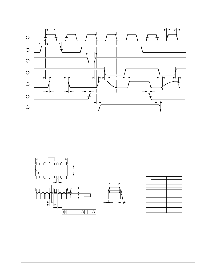
10
DYNAMIC TIMING DIAGRAM
3
15
CLOCK
2
DATA IN
1
STROBE
OUTPUT
ENABLE
N
Q1
│ Q7
9
Q
S
Q
S
t
WH
50%
t
su
t
h
t
WL
50%
t
r
t
f
90%
10%
50%
50%
t
PZL
t
PZH
t
PHZ
t
PHL
t
PLH
t
PLH
t
PLZ
10%
90%
10%
90%
90%
90%
10%
10%
50%
50%
50%
50%
t
PHL
t
PLH
t
THL
t
TLH
t
PLH
t
PHL
PACKAGE DIMENSIONS
PDIP¡16
P SUFFIX
PLASTIC DIP PACKAGE
CASE 648¡08
ISSUE R
NOTES:
1. DIMENSIONING AND TOLERANCING PER ANSI
Y14.5M, 1982.
2. CONTROLLING DIMENSION: INCH.
3. DIMENSION L TO CENTER OF LEADS WHEN
FORMED PARALLEL.
4. DIMENSION B DOES NOT INCLUDE MOLD FLASH.
5. ROUNDED CORNERS OPTIONAL.
¡A¡
B
F
C
S
H
G
D
J
L
M
16 PL
SEATING
1
8
9
16
K
PLANE
¡T¡
M
A
M
0.25 (0.010)
T
DIM
MIN
MAX
MIN
MAX
MILLIMETERS
INCHES
A
0.740
0.770
18.80
19.55
B
0.250
0.270
6.35
6.85
C
0.145
0.175
3.69
4.44
D
0.015
0.021
0.39
0.53
F
0.040
0.70
1.02
1.77
G
0.100 BSC
2.54 BSC
H
0.050 BSC
1.27 BSC
J
0.008
0.015
0.21
0.38
K
0.110
0.130
2.80
3.30
L
0.295
0.305
7.50
7.74
M
0
10
0
10
S
0.020
0.040
0.51
1.01
_
_
_
_
MC14094B
http://onsemi.com
7
PACKAGE DIMENSIONS
SOIC¡16
D SUFFIX
PLASTIC SOIC PACKAGE
CASE 751B¡05
ISSUE J
NOTES:
1. DIMENSIONING AND TOLERANCING PER ANSI
Y14.5M, 1982.
2. CONTROLLING DIMENSION: MILLIMETER.
3. DIMENSIONS A AND B DO NOT INCLUDE
MOLD PROTRUSION.
4. MAXIMUM MOLD PROTRUSION 0.15 (0.006)
PER SIDE.
5. DIMENSION D DOES NOT INCLUDE DAMBAR
PROTRUSION. ALLOWABLE DAMBAR
PROTRUSION SHALL BE 0.127 (0.005) TOTAL
IN EXCESS OF THE D DIMENSION AT
MAXIMUM MATERIAL CONDITION.
1
8
16
9
SEATING
PLANE
F
J
M
R
X 45
_
G
8 PL
P
¡B¡
¡A¡
M
0.25 (0.010)
B
S
¡T¡
D
K
C
16 PL
S
B
M
0.25 (0.010)
A
S
T
DIM
MIN
MAX
MIN
MAX
INCHES
MILLIMETERS
A
9.80
10.00
0.386
0.393
B
3.80
4.00
0.150
0.157
C
1.35
1.75
0.054
0.068
D
0.35
0.49
0.014
0.019
F
0.40
1.25
0.016
0.049
G
1.27 BSC
0.050 BSC
J
0.19
0.25
0.008
0.009
K
0.10
0.25
0.004
0.009
M
0
7
0
7
P
5.80
6.20
0.229
0.244
R
0.25
0.50
0.010
0.019
_
_
_
_
TSSOP¡16
DT SUFFIX
PLASTIC TSSOP PACKAGE
CASE 948F¡01
ISSUE O
╟╟╟
╟╟╟
DIM
MIN
MAX
MIN
MAX
INCHES
MILLIMETERS
A
4.90
5.10
0.193
0.200
B
4.30
4.50
0.169
0.177
C
¡¡¡
1.20
¡¡¡
0.047
D
0.05
0.15
0.002
0.006
F
0.50
0.75
0.020
0.030
G
0.65 BSC
0.026 BSC
H
0.18
0.28
0.007
0.011
J
0.09
0.20
0.004
0.008
J1
0.09
0.16
0.004
0.006
K
0.19
0.30
0.007
0.012
K1
0.19
0.25
0.007
0.010
L
6.40 BSC
0.252 BSC
M
0
8
0
8
NOTES:
1.
DIMENSIONING AND TOLERANCING PER ANSI
Y14.5M, 1982.
2.
CONTROLLING DIMENSION: MILLIMETER.
3.
DIMENSION A DOES NOT INCLUDE MOLD
FLASH. PROTRUSIONS OR GATE BURRS. MOLD
FLASH OR GATE BURRS SHALL NOT EXCEED 0.15
(0.006) PER SIDE.
4.
DIMENSION B DOES NOT INCLUDE INTERLEAD
FLASH OR PROTRUSION. INTERLEAD FLASH OR
PROTRUSION SHALL NOT EXCEED
0.25 (0.010) PER SIDE.
5.
DIMENSION K DOES NOT INCLUDE DAMBAR
PROTRUSION. ALLOWABLE DAMBAR
PROTRUSION SHALL BE 0.08 (0.003) TOTAL IN
EXCESS OF THE K DIMENSION AT MAXIMUM
MATERIAL CONDITION.
6.
TERMINAL NUMBERS ARE SHOWN FOR
REFERENCE ONLY.
7.
DIMENSION A AND B ARE TO BE DETERMINED
AT DATUM PLANE ¡W¡.
_
_
_
_
SECTION N¡N
SEATING
PLANE
IDENT.
PIN 1
1
8
16
9
DETAIL E
J
J1
B
C
D
A
K
K1
H
G
╔╔
╔╔
DETAIL E
F
M
L
2X
L/2
¡U¡
S
U
0.15 (0.006) T
S
U
0.15 (0.006) T
S
U
M
0.10 (0.004)
V
S
T
0.10 (0.004)
¡T¡
¡V¡
¡W¡
0.25 (0.010)
16X REF
K
N
N
MC14094B
http://onsemi.com
8
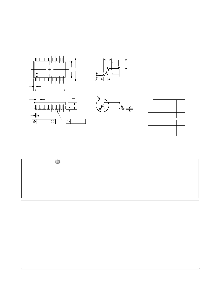
PACKAGE DIMENSIONS
H
E
A
1
DIM
MIN
MAX
MIN
MAX
INCHES
¡¡¡
2.05
¡¡¡
0.081
MILLIMETERS
0.05
0.20
0.002
0.008
0.35
0.50
0.014
0.020
0.18
0.27
0.007
0.011
9.90
10.50
0.390
0.413
5.10
5.45
0.201
0.215
1.27 BSC
0.050 BSC
7.40
8.20
0.291
0.323
0.50
0.85
0.020
0.033
1.10
1.50
0.043
0.059
0
0.70
0.90
0.028
0.035
¡¡¡
0.78
¡¡¡
0.031
A
1
H
E
Q
1
L
E
_
10
_
0
_
10
_
L
E
Q
1
_
NOTES:
1.
DIMENSIONING AND TOLERANCING PER ANSI
Y14.5M, 1982.
2.
CONTROLLING DIMENSION: MILLIMETER.
3.
DIMENSIONS D AND E DO NOT INCLUDE
MOLD FLASH OR PROTRUSIONS AND ARE
MEASURED AT THE PARTING LINE. MOLD FLASH
OR PROTRUSIONS SHALL NOT EXCEED 0.15
(0.006) PER SIDE.
4.
TERMINAL NUMBERS ARE SHOWN FOR
REFERENCE ONLY.
5.
THE LEAD WIDTH DIMENSION (b) DOES NOT
INCLUDE DAMBAR PROTRUSION. ALLOWABLE
DAMBAR PROTRUSION SHALL BE 0.08 (0.003)
TOTAL IN EXCESS OF THE LEAD WIDTH
DIMENSION AT MAXIMUM MATERIAL CONDITION.
DAMBAR CANNOT BE LOCATED ON THE LOWER
RADIUS OR THE FOOT. MINIMUM SPACE
BETWEEN PROTRUSIONS AND ADJACENT LEAD
TO BE 0.46 ( 0.018).
M
L
DETAIL P
VIEW P
c
A
b
e
M
0.13 (0.005)
0.10 (0.004)
1
16
9
8
D
Z
E
A
b
c
D
E
e
L
M
Z
SOEIAJ¡16
F SUFFIX
PLASTIC EIAJ SOIC PACKAGE
CASE 966¡01
ISSUE O
ON Semiconductor and are trademarks of Semiconductor Components Industries, LLC (SCILLC). SCILLC reserves the right to make changes
without further notice to any products herein. SCILLC makes no warranty, representation or guarantee regarding the suitability of its products for any particular
purpose, nor does SCILLC assume any liability arising out of the application or use of any product or circuit, and specifically disclaims any and all liability,
including without limitation special, consequential or incidental damages. "Typical" parameters which may be provided in SCILLC data sheets and/or
specifications can and do vary in different applications and actual performance may vary over time. All operating parameters, including "Typicals" must be
validated for each customer application by customer's technical experts. SCILLC does not convey any license under its patent rights nor the rights of others.
SCILLC products are not designed, intended, or authorized for use as components in systems intended for surgical implant into the body, or other applications
intended to support or sustain life, or for any other application in which the failure of the SCILLC product could create a situation where personal injury or
death may occur. Should Buyer purchase or use SCILLC products for any such unintended or unauthorized application, Buyer shall indemnify and hold
SCILLC and its officers, employees, subsidiaries, affiliates, and distributors harmless against all claims, costs, damages, and expenses, and reasonable
attorney fees arising out of, directly or indirectly, any claim of personal injury or death associated with such unintended or unauthorized use, even if such claim
alleges that SCILLC was negligent regarding the design or manufacture of the part. SCILLC is an Equal Opportunity/Affirmative Action Employer.
PUBLICATION ORDERING INFORMATION
CENTRAL/SOUTH AMERICA:
Spanish Phone: 303¡308¡7143 (Mon¡Fri 8:00am to 5:00pm MST)
Email: ONlit¡spanish@hibbertco.com
ASIA/PACIFIC: LDC for ON Semiconductor ¡ Asia Support
Phone: 303¡675¡2121 (Tue¡Fri 9:00am to 1:00pm, Hong Kong Time)
Toll Free from Hong Kong & Singapore:
001¡800¡4422¡3781
Email: ONlit¡asia@hibbertco.com
JAPAN: ON Semiconductor, Japan Customer Focus Center
4¡32¡1 Nishi¡Gotanda, Shinagawa¡ku, Tokyo, Japan 141¡8549
Phone: 81¡3¡5740¡2745
Email: r14525@onsemi.com
ON Semiconductor Website: http://onsemi.com
For additional information, please contact your local
Sales Representative.
MC14094B/D
NORTH AMERICA Literature Fulfillment:
Literature Distribution Center for ON Semiconductor
P.O. Box 5163, Denver, Colorado 80217 USA
Phone: 303¡675¡2175 or 800¡344¡3860 Toll Free USA/Canada
Fax: 303¡675¡2176 or 800¡344¡3867 Toll Free USA/Canada
Email: ONlit@hibbertco.com
Fax Response Line: 303¡675¡2167 or 800¡344¡3810 Toll Free USA/Canada
N. American Technical Support: 800¡282¡9855 Toll Free USA/Canada
EUROPE: LDC for ON Semiconductor ¡ European Support
German Phone: (+1) 303¡308¡7140 (M¡F 1:00pm to 5:00pm Munich Time)
Email: ONlit¡german@hibbertco.com
French Phone: (+1) 303¡308¡7141 (M¡F 1:00pm to 5:00pm Toulouse Time)
Email: ONlit¡french@hibbertco.com
English Phone: (+1) 303¡308¡7142 (M¡F 12:00pm to 5:00pm UK Time)
Email: ONlit@hibbertco.com
EUROPEAN TOLL¡FREE ACCESS*: 00¡800¡4422¡3781
*Available from Germany, France, Italy, England, Ireland