©
Semiconductor Components Industries, LLC, 2000
March, 2000 ≠ Rev. 3
1
Publication Order Number:
MC14512B/D
MC14512B
8-Channel Data Selector
The MC14512B is an 8≠channel data selector constructed with
MOS P≠channel and N≠channel enhancement mode devices in a
single monolithic structure. This data selector finds primary
application in signal multiplexing functions. It may also be used for
data routing, digital signal switching, signal gating, and number
sequence generation.
∑
Diode Protection on All Inputs
∑
Single Supply Operation
∑
3≠State Output (Logic "1", Logic "0", High Impedance)
∑
Supply Voltage Range = 3.0 Vdc to 18 Vdc
∑
Capable of Driving Two Low≠power TTL Loads or One Low≠power
Schottky TTL Load Over the Rated Temperature Range
MAXIMUM RATINGS
(Voltages Referenced to V
SS
) (Note 2.)
Symbol
Parameter
Value
Unit
V
DD
DC Supply Voltage Range
≠ 0.5 to +18.0
V
V
in
, V
out
Input or Output Voltage Range
(DC or Transient)
≠ 0.5 to V
DD
+ 0.5
V
I
in
, I
out
Input or Output Current
(DC or Transient) per Pin
±
10
mA
P
D
Power Dissipation,
per Package (Note NO TAG)
500
mW
T
A
Ambient Temperature Range
≠ 55 to +125
∞
C
T
stg
Storage Temperature Range
≠ 65 to +150
∞
C
T
L
Lead Temperature
(8≠Second Soldering)
260
∞
C
2. Maximum Ratings are those values beyond which damage to the device
may occur.
3. Temperature Derating:
Plastic "P and D/DW" Packages: ≠ 7.0 mW/
_
C From 65
_
C To 125
_
C
This device contains protection circuitry to guard against damage due to high
static voltages or electric fields. However, precautions must be taken to avoid
applications of any voltage higher than maximum rated voltages to this
high≠impedance circuit. For proper operation, V
in
and V
out
should be constrained
to the range V
SS
v
(V
in
or V
out
)
v
V
DD
.
Unused inputs must always be tied to an appropriate logic voltage level (e.g.,
either V
SS
or V
DD
). Unused outputs must be left open.
http://onsemi.com
A
= Assembly Location
WL or L
= Wafer Lot
YY or Y
= Year
WW or W = Work Week
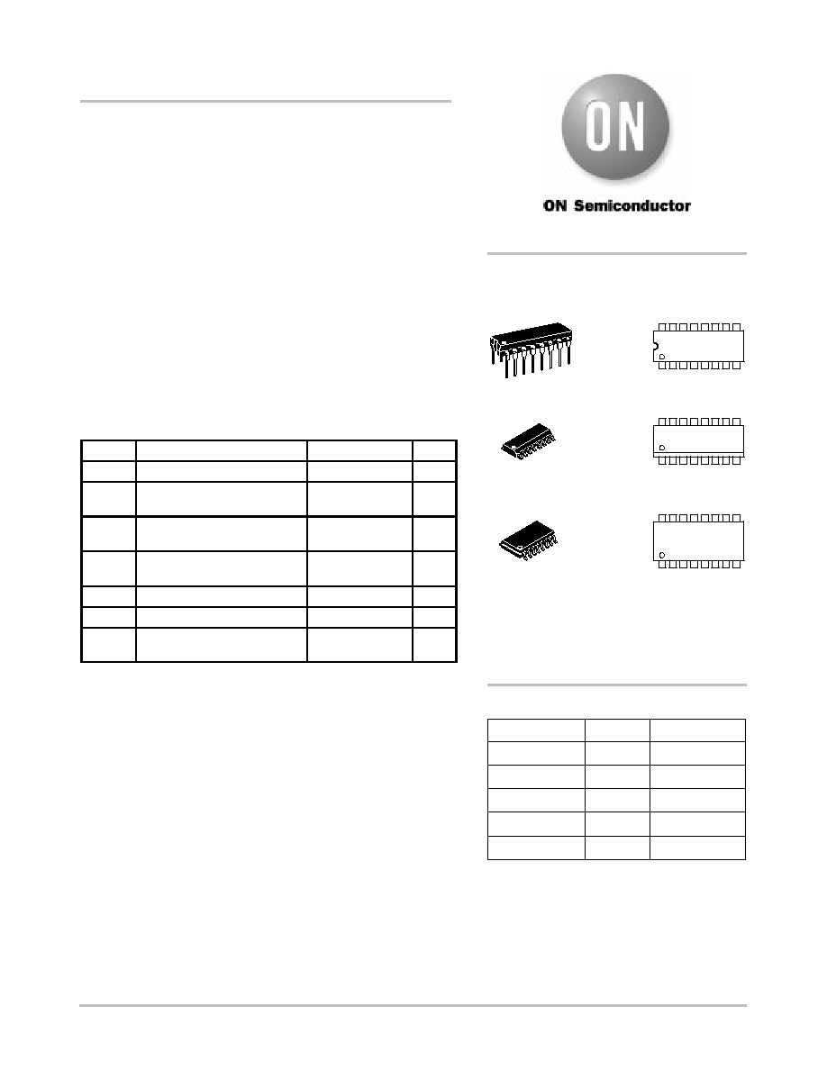
Device
Package
Shipping
ORDERING INFORMATION
MC14512BCP
PDIP≠16
2000/Box
MC14512BD
SOIC≠16
48/Rail
MC14512BDR2
SOIC≠16
2500/Tape & Reel
1. For ordering information on the EIAJ version of
the SOIC packages, please contact your local
ON Semiconductor representative.
MARKING
DIAGRAMS
1
16
PDIP≠16
P SUFFIX
CASE 648
MC14512BCP
AWLYYWW
SOIC≠16
D SUFFIX
CASE 751B
1
16
14512B
AWLYWW
SOEIAJ≠16
F SUFFIX
CASE 966
1
16
MC14512B
AWLYWW
MC14512BF
SOEIAJ≠16
See Note 1.
MC14512BFL1
SOEIAJ≠16
See Note 1.

MC14512B
http://onsemi.com
3
ŒŒŒŒŒŒŒŒŒŒŒŒŒŒŒŒŒŒŒŒŒŒŒŒŒŒŒŒŒŒŒŒŒ
ŒŒŒŒŒŒŒŒŒŒŒŒŒŒŒŒŒŒŒŒŒŒŒŒŒŒŒŒŒŒŒŒŒ
ELECTRICAL CHARACTERISTICS
(Voltages Referenced to V
SS
)
V
DD
≠ 55
_
C
25
_
C
125
_
C
Characteristic
Symbol
V
DD
Vdc
Min
Max
Min
Typ
(4.)
Max
Min
Max
Unit
Output Voltage
"0" Level
V
in
= V
DD
or 0
V
OL
5.0
10
15
--
--
--
0.05
0.05
0.05
--
--
--
0
0
0
0.05
0.05
0.05
--
--
--
0.05
0.05
0.05
Vdc
"1" Level
V
in
= 0 or V
DD
V
OH
5.0
10
15
4.95
9.95
14.95
--
--
--
4.95
9.95
14.95
5.0
10
15
--
--
--
4.95
9.95
14.95
--
--
--
Vdc
Input Voltage
"0" Level
(V
O
= 4.5 or 0.5 Vdc)
(V
O
= 9.0 or 1.0 Vdc)
(V
O
= 13.5 or 1.5 Vdc)
V
IL
5.0
10
15
--
--
--
1.5
3.0
4.0
--
--
--
2.25
4.50
6.75
1.5
3.0
4.0
--
--
--
1.5
3.0
4.0
Vdc
"1" Level
(V
O
= 0.5 or 4.5 Vdc)
(V
O
= 1.0 or 9.0 Vdc)
(V
O
= 1.5 or 13.5 Vdc)
V
IH
5.0
10
15
3.5
7.0
11
--
--
--
3.5
7.0
11
2.75
5.50
8.25
--
--
--
3.5
7.0
11
--
--
--
Vdc
Output Drive Current
(V
OH
= 2.5 Vdc)
Source
(V
OH
= 4.6 Vdc)
(V
OH
= 9.5 Vdc)
(V
OH
= 13.5 Vdc)
I
OH
5.0
5.0
10
15
≠ 3.0
≠ 0.64
≠ 1.6
≠ 4.2
--
--
--
--
≠ 2.4
≠ 0.51
≠ 1.3
≠ 3.4
≠ 4.2
≠ 0.88
≠ 2.25
≠ 8.8
--
--
--
--
≠ 1.7
≠ 0.36
≠ 0.9
≠ 2.4
--
--
--
--
mAdc
(V
OL
= 0.4 Vdc)
Sink
(V
OL
= 0.5 Vdc)
(V
OL
= 1.5 Vdc)
I
OL
5.0
10
15
0.64
1.6
4.2
--
--
--
0.51
1.3
3.4
0.88
2.25
8.8
--
--
--
0.36
0.9
2.4
--
--
--
mAdc
Input Current
I
in
15
--
±
0.1
--
±
0.00001
±
0.1
--
±
1.0
µ
Adc
Input Capacitance
(V
in
= 0)
C
in
--
--
--
--
5.0
7.5
--
--
pF
Quiescent Current
(Per Package)
I
DD
5.0
10
15
--
--
--
5.0
10
20
--
--
--
0.005
0.010
0.015
5.0
10
20
--
--
--
150
300
600
µ
Adc
Total Supply Current
(5.) (6.)
(Dynamic plus Quiescent,
Per Package)
(C
L
= 50 pF on all outputs, all
buffers switching)
I
T
5.0
10
15
I
T
= (0.8
µ
A/kHz) f + I
DD
I
T
= (1.6
µ
A/kHz) f + I
DD
I
T
= (2.4
µ
A/kHz) f + I
DD
µ
Adc
Three≠State Leakage Current
I
TL
15
--
±
0.1
--
±
0.0001
±
0.1
--
±
3.0
µ
Adc
4. Data labelled "Typ" is not to be used for design purposes but is intended as an indication of the IC's potential performance.
5. The formulas given are for the typical characteristics only at 25
_
C.
6. To calculate total supply current at loads other than 50 pF:
I
T
(C
L
) = I
T
(50 pF) + (C
L
≠ 50) Vfk
where: I
T
is in
µ
A (per package), C
L
in pF, V = (V
DD
≠ V
SS
) in volts, f in kHz is input frequency, and k = 0.001.

MC14512B
http://onsemi.com
4
SWITCHING CHARACTERISTICS
(7.)
(C
L
= 50 pF, T
A
= 25
_
C, See Figure 1)
All Types
Characteristic
Symbol
V
DD
Typ
(8.)
Max
Unit
Output Rise and Fall Time
t
TLH
, t
THL
= (1.5 ns/pF) C
L
+ 25 ns
t
TLH
, t
THL
= (0.75 ns/pF) C
L
+ 12.5 ns
t
TLH
, t
THL
= (0.55 ns/pF) C
L
+ 9.5 ns
t
TLH
,
t
THL
5.0
10
15
100
50
40
200
100
80
ns
Propagation Delay Time (Figure 2)
Inhibit, Control, or Data to Z
t
PLH
5.0
10
15
330
125
85
650
250
170
ns
Propagation Delay Time (Figure 2)
Inhibit, Control, or Data to Z
t
PHL
5.0
10
15
330
125
85
650
250
170
ns
3≠State Output Delay Times (Figure 3)
"1" or "0" to High Z, and
High Z to "1" or "0"
t
PHZ
, t
PLZ
,
t
PZH
, t
PZL
5.0
10
15
60
35
30
150
100
75
ns
7. The formulas given are for the typical characteristics only at 25
_
C.
8. Data labelled "Typ" is not to be used for design purposes but is intended as an indication of the IC's potential performance.
Figure 1. Power Dissipation Test Circuit and Waveform
V
DD
I
D
C
L
Z
DISABLE
INHIBIT
A
B
C
X0
X1
X2
X3
X4
X5
X6
X7
V
SS
PULSE
GENERATOR
50%
V
in
50%
DUTY
CYCLE

MC14512B
http://onsemi.com
5
Parameter
Test Conditions
Inhibit to Z
A, B, C = V
SS
, X
O
= V
DD
A, B, C to Z
Inh = V
SS
, X
O
= V
DD
Figure 2. AC Test Circuit and Waveforms
V
DD
V
SS
V
OH
V
OL
V
DD
V
SS
V
OH
V
OL
V
DD
C
L
Z
DISABLE
INHIBIT
A
B
C
X0
X1
X2
X3
X4
X5
X6
X7
V
SS
PULSE
GENERATOR
20 ns
20 ns
90%
50%
10%
t
PLH
t
PHL
90%
10%
50%
DATA
Z
t
TLH
t
THL
TEST CONDITIONS:
INHIBIT = V
SS
A, B, C = V
SS
20 ns
20 ns
t
PHL
t
PLH
50%
90%
10%
t
THL
t
TLH
Z
INHIBIT,
A, B, OR C
90%
50%
10%
Figure 3. 3≠State AC Test Circuit and Waveform
Test
S1
S2
S3
S4
t
PHZ
Open
Closed
Closed
Open
t
PLZ
Closed
Open
Open
Closed
t
PZL
Closed
Open
Open
Closed
t
PZH
Open
Closed
Closed
Open
Switch Positions for 3≠State Test
Z
DISABLE
INHIBIT
A
B
C
X0
X1
X2
X3
X4
X5
X6
X7
V
SS
PULSE
GENERATOR
V
DD
V
DD
C
L
1 k
S1
S2
V
SS
V
DD
S3
S4
V
SS
V
DD
V
OH
V
OL
20 ns
90%
50%
10%
t
PLZ
t
PZL
20 ns
DISABLE
INPUT
OUTPUT
OUTPUT
V
SS
V
OH
V
OL
10%
90%
90%
10%
t
PHZ
t
PZH
2.5 V @ V
DD
= 5 V,
10 V, AND 15 V
2 V @ V
DD
= 5 V
6 V @ V
DD
= 10 V
10 V @ V
DD
= 15 V
