 | ÐлекÑÑоннÑй компоненÑ: MC34064 | СкаÑаÑÑ:  PDF PDF  ZIP ZIP |
Äîêóìåíòàöèÿ è îïèñàíèÿ www.docs.chipfind.ru
©
Semiconductor Components Industries, LLC, 2005
February, 2005 - Rev. 12
1
Publication Order Number:
MC34064/D
MC34064, MC33064,
NCV33064
Undervoltage Sensing
Circuit
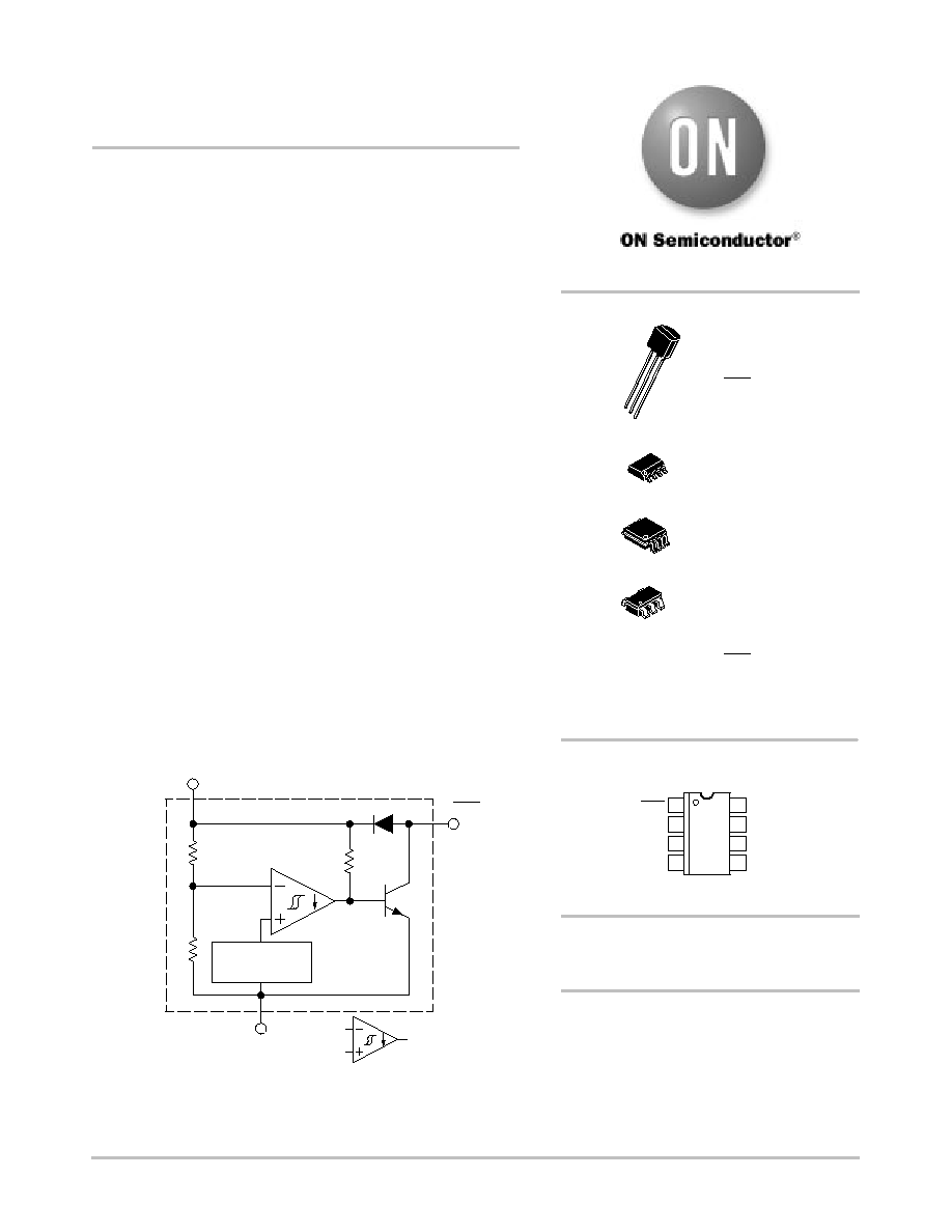
The MC34064 is an undervoltage sensing circuit specifically
designed for use as a reset controller in microprocessor-based
systems. It offers the designer an economical solution for low voltage
detection with a single external resistor. The MC34064 features a
trimmed-in-package bandgap reference, and a comparator with
precise thresholds and built-in hysteresis to prevent erratic reset
operation. The open collector reset output is capable of sinking in
excess of 10 mA, and operation is guaranteed down to 1.0 V input with
low standby current. The MC devices are packaged in 3-pin TO-92,
micro size TSOP-5, 8-pin SOIC-8 and Micro8
t surface mount
packages. The NCV device is packaged in SOIC-8 and TO-92.
Applications include direct monitoring of the 5.0 V MPU/logic
power supply used in appliance, automotive, consumer and industrial
equipment.
Features
·
Trimmed-In-Package Temperature Compensated Reference
·
Comparator Threshold of 4.6 V at 25
°
C
·
Precise Comparator Thresholds Guaranteed Over Temperature
·
Comparator Hysteresis Prevents Erratic Reset
·
Reset Output Capable of Sinking in Excess of 10 mA
·
Internal Clamp Diode for Discharging Delay Capacitor
·
Guaranteed Reset Operation with 1.0 V Input
·
Low Standby Current
·
Economical TO-92, TSOP-5, SOIC-8 and Micro8 Surface Mount
Packages
·
NCV Prefix for Automotive and Other Applications Requiring Site
and Control Changes
·
Pb-Free Packages are Available
1.2 V
ref
2 (2)
1 (1)
3 (4)
Reset
GND
Input
=
Sink Only
Positive True Logic
Pin numbers adjacent to terminals are for the 3-pin TO-92 package.
Pin numbers in parenthesis are for the 8-lead packages.
This device contains 21 active transistors.
Figure 1. Representative Block Diagram
http://onsemi.com
1
2
3
Pin 1. Reset
2. Input
3. Ground
TO-92
P SUFFIX
CASE 29
8
1
(Top View)
3
1
N.C.
Ground
N.C.
N.C.
2
4
8
7
6
5
N.C.
N.C.
Input
Reset
8
1
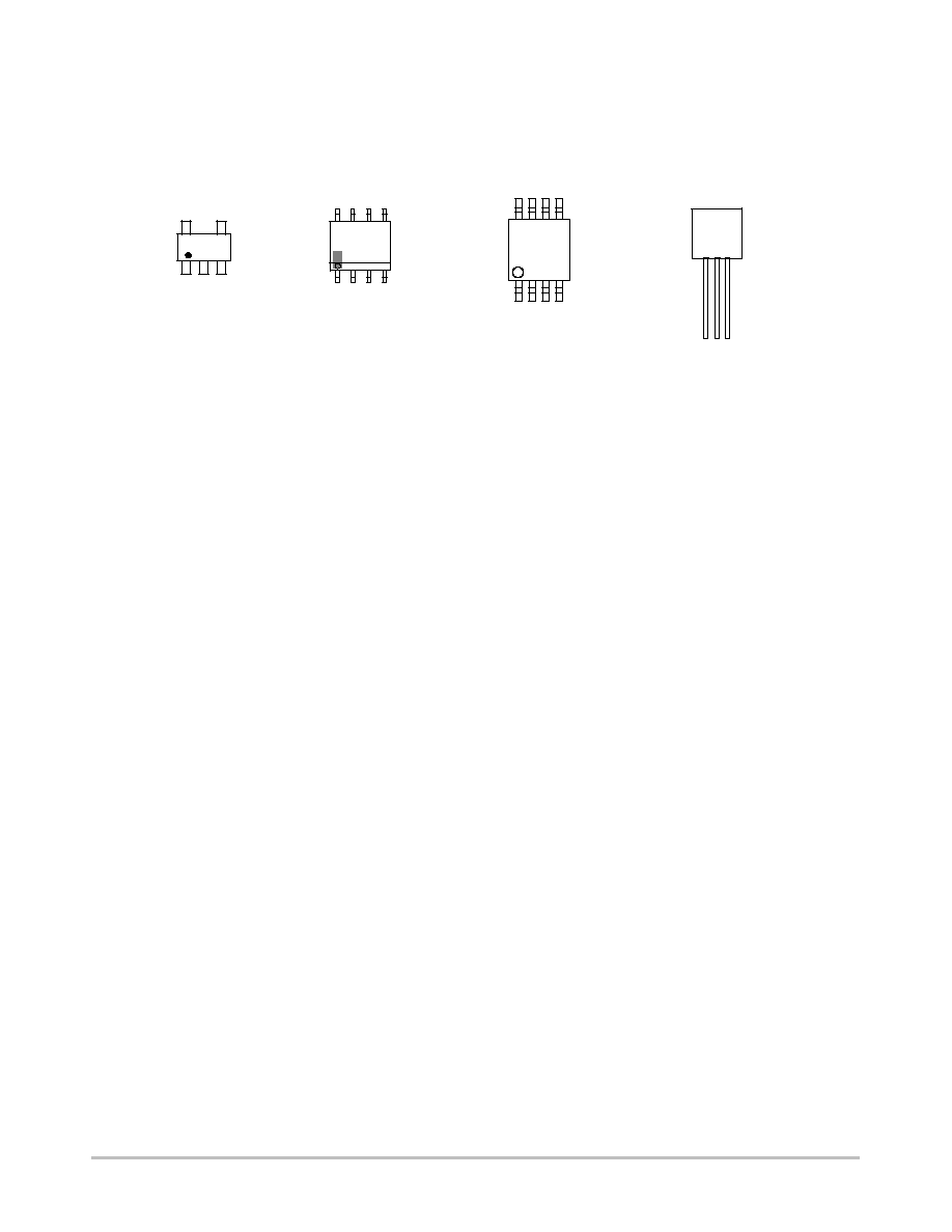
PIN CONNECTIONS
ORDERING INFORMATION
SOIC-8
D SUFFIX
CASE 751
Micro8
DM SUFFIX
CASE 846A
TSOP-5
SN SUFFIX
CASE 483
1
5
Pin 1. Reset
2. Input
3. Ground
4. NC
5. NC
See detailed ordering and shipping information in the package
dimensions section on page 6 of this data sheet.
See general marking information in the device marking
section on page 7 of this data sheet.
DEVICE MARKING INFORMATION
MC34064, MC33064, NCV33064
http://onsemi.com
2
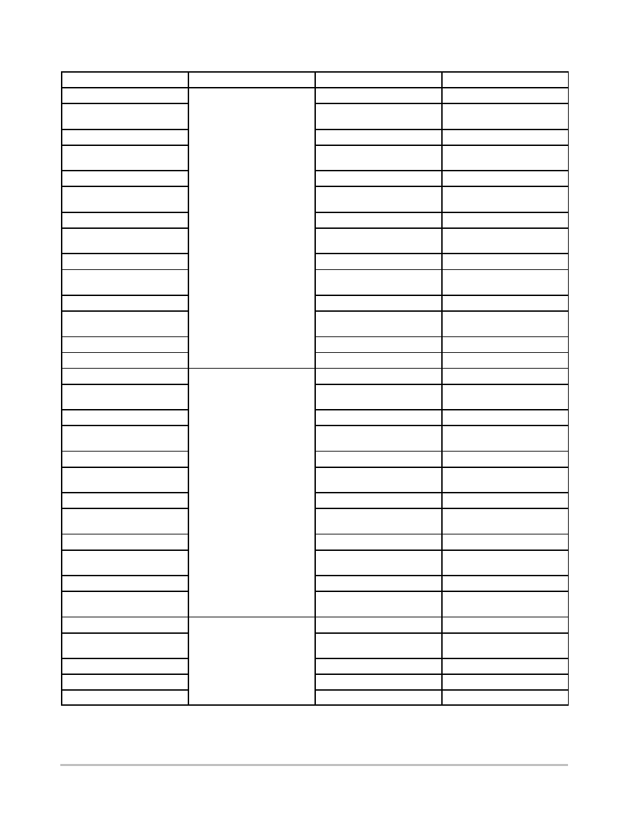
MAXIMUM RATINGS
Rating
Symbol
Value
Unit
Power Input Supply Voltage
V
in
-1.0 to 10
V
Reset Output Voltage
V
O
10
V
Reset Output Sink Current (Note 2)
I
Sink
Internally
Limited
mA
Clamp Diode Forward Current, Pin 1 to 2 (Note 2)
I
F
100
mA
Power Dissipation and Thermal Characteristics
P Suffix, Plastic Package
Maximum Power Dissipation @ T
A
= 25
°
C
Thermal Resistance, Junction-to-Air
D Suffix, Plastic Package
Maximum Power Dissipation @ T
A
= 25
°
C
Thermal Resistance, Junction-to-Air
DM Suffix, Plastic Package
Maximum Power Dissipation @ T
A
= 25
°
C
Thermal Resistance, Junction-to-Air
P
D
R
q
JA
P
D
R
q
JA
P
D
R
q
JA
625
200
625
200
520
240
mW
°
C/W
mW
°
C/W
mW
°
C/W
Operating Junction Temperature
T
J
+150
°
C
Operating Ambient Temperature
MC34064
MC33064
NCV33064
T
A
0 to +70
-40 to +85
-40 to +125
°
C
Storage Temperature Range
T
stg
-65 to +150
°
C
Maximum ratings are those values beyond which device damage can occur. Maximum ratings applied to the device are individual stress limit
values (not normal operating conditions) and are not valid simultaneously. If these limits are exceeded, device functional operation is not implied,
damage may occur and reliability may be affected.
1. ESD data available upon request.
ELECTRICAL CHARACTERISTICS
(For typical values T
A
= 25
°
C, for min/max values T
A
is the operating ambient temperature range
that applies [Notes 3 and 4] unless otherwise noted.)
Characteristics
Symbol
Min
Typ
Max
Unit
COMPARATOR
Threshold Voltage
High State Output (V
in
Increasing)
Low State Output (V
in
Decreasing)
Hysteresis
V
IH
V
IL
V
H
4.5
4.5
0.01
4.61
4.59
0.02
4.7
4.7
0.05
V
RESET OUTPUT
Output Sink Saturation
(V
in
= 4.0 V, I
Sink
= 8.0 mA)
(V
in
= 4.0 V, I
Sink
= 2.0 mA)
(V
in
= 1.0 V, I
Sink
= 0.1 mA)
V
OL
-
-
-
0.46
0.15
-
1.0
0.4
0.1
V
Output Sink Current (V
in
, Reset = 4.0 V)
I
Sink
10
27
60
mA
Output Off-State Leakage (V
in
, Reset = 5.0 V)
I
OH
-
0.02
0.5
m
A
Clamp Diode Forward Voltage, Pin 1 to 2 (I
F
= 10 mA)
V
F
0.6
0.9
1.2
V
TOTAL DEVICE
Operating Input Voltage Range
V
in
1.0 to 6.5
-
-
V
Quiescent Input Current (V
in
= 5.0 V)
I
in
-
390
500
m
A
2. Maximum package power dissipation limits must be observed.
3. Low duty cycle pulse techniques are used during test to maintain junction temperature as close to ambient as possible.
4. T
low
= 0
°
C for MC34064
T
high
= +70
°
C for MC34064
-40
°
C for MC33064
+85
°
C for MC33064
-40
°
C for NCV33064
+125
°
C for NCV33064
5. NCV prefix is for automotive and other applications requiring site and change control.
MC34064, MC33064, NCV33064
http://onsemi.com
3
V
O
, OUTPUT
VOL
T
AGE (V)
V
O
, OUTPUT
VOL
T
AGE (V)
Figure 2. Reset Output Voltage versus
Input Voltage
Figure 3. Reset Output Voltage versus
Input Voltage
Figure 4. Comparator Threshold Voltage
versus Temperature
Figure 5. Input Current versus Input Voltage
Figure 6. Reset Output Saturation versus
Sink Current
Figure 7. Reset Delay Time
V
in
, INPUT VOLTAGE (V)
10
8.0
6.0
4.0
2.0
0
0
2.0
4.0
6.0
8.0
10
R
L
= 10 k to V
in
T
A
= 25
°
C
V
in
, INPUT VOLTAGE (V)
5.0
4.0
3.0
2.0
1.0
0
4.560
4.580
4.600
4.620
4.640
R
L
= 10 k to V
in
T
A
= 25
°
C
T
A
, AMBIENT TEMPERATURE (
°
C)
th
,
THRESHOLD VOL
T
AGE (V)
4.630
4.620
4.610
4.600
4.590
4.580
4.570
-55
-25
0
25
50
75
100
125
V
R
L
= 10 k to V
in
Upper Threshold
High State Output
Lower Threshold
Low State Output
V
in
, INPUT VOLTAGE (V)
in
, INPUT
CURRENT
(mA)
1.0
0.8
0.6
0.4
0.2
0
0
2.0
4.0
6.0
8.0
10
I
T
A
= +25
°
C
-40
°
C
T
A
= +25
°
C
+85
°
C
-40
°
C
V
OL
, OUTPUT
SA
TURA
TION (V)
I
Sink
, SINK CURRENT (mA)
2.0
1.5
1.0
0.5
0
0
10
20
30
40
V
in
= 4.0 V
T
A
= 85
°
C
T
A
= 25
°
C
T
A
= -40
°
C
90%
5.0 V -
4.0 V -
10%
+85
°
C
Reset
V
in
5.0V
4.0V
REF
10k
200 ns/DIV
Reset
V
in
V
in
= 5.0 V to 4.0 V
R
L
= 10 k
T
A
= 25
°
C
MC34064, MC33064, NCV33064
http://onsemi.com
4
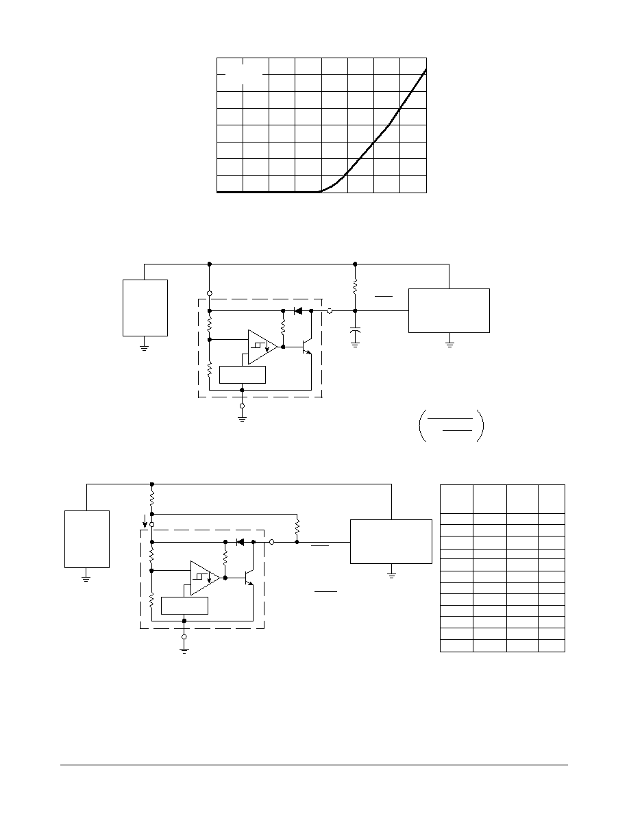
Figure 8. Clamp Diode Forward Current versus Voltage
Figure 9. Low Voltage Microprocessor Reset
Figure 10. Low Voltage Microprocessor Reset with Additional Hysteresis
80
60
40
20
0
0
0.4
0.8
1.2
1.6
V
F
, FORWARD VOLTAGE (V)
, FOR
W
ARD CURRENT
(mA)
FI
V
in
= 0 V
T
A
= 25
°
C
A time delayed reset can be accomplished with the
addition of C
DLY
. For systems with extremely fast
power supply rise times (<500 ns) it is recommended
that the RC
DLY
time constant be greater than 5.0
ms.
V
th(MPU)
is the microprocessor reset input threshold.
t
DLY
= RC
DLY
In
1
1 -
V
th(MPU)
Power
Supply
+
-
2 (2)
R
1 (1)
Reset
C
DLY
Microprocessor
Circuit
1.2 V
ref
3 (4)
-
+
Power
Supply
+
-
2 (2)
R
L
1 (1)
Reset
Microprocessor
Circuit
1.2V
ref
3 (4)
-
+
V
H
4.6 R
H
+ 0.02
DV
th(lower)
340 R
H
x 10
-6
Where: R
H
150
W
Where:
R
L
1.5
W,
10 k
W
Comparator hysteresis can be increased with the addition of resistor R
H
. The hysteresis equation has been
simplified and does not account for the change of input current I
in
as V
CC
crosses the comparator threshold
(Figure 4). An increase of the lower threshold
DV
th(lower)
will be observed due to I
in
which is typically 340
mA at
4.59 V. The equations are accurate to
±
10% with R
H
less than 150
W and R
L
between 1.5 k
W and 10 kW.
I
in
R
H
V
in
R
L
TEST DATA
V
H
(mV)
D
V
th
(mV)
R
H
(
W
)
R
L
(k
W
)
20
51
40
81
71
112
100
164
190
327
276
480
0
3.4
6.8
6.8
10
10
16
16
34
34
51
51
0
10
20
20
30
30
47
47
100
100
150
150
0
1.5
4.7
1.5
2.7
1.5
2.7
1.5
2.7
1.5
2.7
1.5
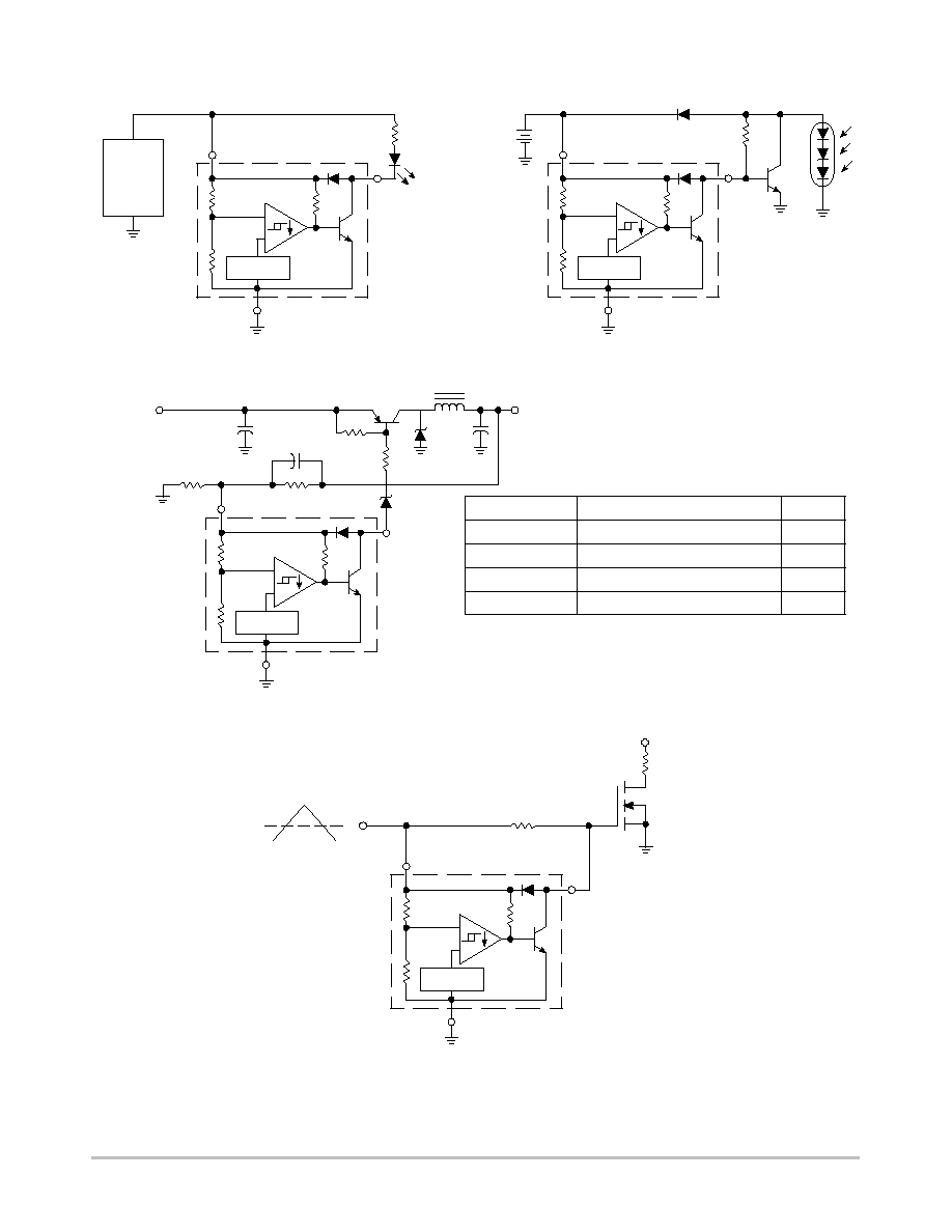
Figure 11. Voltage Monitor
Figure 12. Solar Powered Battery Charger
Figure 13. Low Power Switching Regulator
Figure 14. MOSFET Low Voltage Gate Drive Protection
Overheating of the logic level power MOSFET due to insufficient gate voltage can be prevented with the above
circuit. When the input signal is below the 4.6 V threshold of the MC34064, its output grounds the gate of the L
2
MOSFET.
270
4.6V
V
CC
R
L
MTP3055EL
2 (2)
1 (1)
3 (4)
-
+
1.2V
ref
2 (2)
1 (1)
3 (4)
-
+
1.2V
ref
Power
Supply
+
-
1.0k
2 (2)
1 (1)
3 (4)
-
+
1.2V
ref
+
-
Solar
Cells
2 (2)
1 (1)
3 (4)
-
+
1.2V
ref
V
in
= 11.5
to 14.5V
470
+
MPSW51A
25
mH
V
O
= 5.0 V
I
O
= 50 mA
470
+
680
22
+
1N5819
1.2k
330
1N756
4.7k
MC34064, MC33064, NCV33064
http://onsemi.com
5
Test
Conditions
Results
Line Regulation
V
in
= 11.5 V to 14.5 V, I
O
= 50 mA
35 mV
Load Regulation
V
in
= 12.6 V, I
O
= 0 mA to 50 mA
12 mV
Output Ripple
V
in
= 12.6 V, I
O
= 50 mA
60 mVpp
Efficiency
V
in
= 12.6 V, I
O
= 50 mA
77%
MC34064, MC33064, NCV33064
http://onsemi.com
6
ORDERING INFORMATION
Device
Operating Temperature Range
Package
Shipping
MC34064D-005
SOIC-8
98 Units / Rail
MC34064D-005G
SOIC-8
(Pb-Free)
98 Units / Rail
MC34064D-5R2
SOIC-8
2500 Units/ Tape & Reel
MC34064D-5R2G
SOIC-8
(Pb-Free)
2500 Units/ Tape & Reel
MC34064DM-5R2
Micro8
4000 Units / Tape & Reel
MC34064DM-5R2G
Micro8
(Pb-Free)
4000 Units / Tape & Reel
MC34064P-005
T
0
°
C to +70
°
C
TO-92
2000 Units / Bag
MC34064P-005G
T
A
= 0
°
C to +70
°
C
TO-92
(Pb-Free)
2000 Units / Bag
MC34064P-5RA
TO-92
2000 Units / Tape & Reel
MC34064P-5RAG
TO-92
(Pb-Free)
2000 Units / Tape & Reel
MC34064P-5RP
TO-92
2000 Units / Ammo Pack
MC34064P-5RPG
TO-92
(Pb-Free)
2000 Units / Ammo Pack
MC34064P-5RM
TO-92
2000 Units / Ammo Pack
MC34064SN-5T1
TSOP-5
3000 Units / Tape & Reel
MC33064D-005
SOIC-8
98 Units / Rail
MC33064D-005G
SOIC-8
(Pb-Free)
98 Units / Rail
MC33064D-5R2
SOIC-8
2500 Units / Tape & Reel
MC33064D-5R2G
SOIC-8
(Pb-Free)
2500 Units / Tape & Reel
MC33064DM-5R2
Micro8
4000 Units / Tape & Reel
MC33064DM-5R2G
T = 40
°
C to +85
°
C
Micro8
(Pb-Free)
4000 Units / Tape & Reel
MC33064P-005
T
J
= -40
°
C to +85
°
C
TO-92
2000 Units / Bag
MC33064P-005G
TO-92
(Pb-Free)
2000 Units / Bag
MC33064P-5RA
TO-92
2000 Units / Tape & Reel
MC33064P-5RAG
TO-92
(Pb-Free)
2000 Units / Tape & Reel
MC33064P-5RP
TO-92
2000 Units / Ammo Pack
MC33064P-5RPG
TO-92
(Pb-Free)
2000 Units / Ammo Pack
NCV33064D-5R2*
SOIC-8
2500 Units / Tape & Reel
NCV33064D-5R2G*
SOIC-8
(Pb-Free)
2500 Units / Tape & Reel
NCV33064P-5RA*
T
A
= -40
°
C to +125
°
C
TO-92
2000 Units / Tape & Reel
NCV33064P-5RP*
TO-92
2000 Units / Ammo Pack
NCV33064DM-5R2*
Micro8
4000 Units / Tape & Reel
*NCV33064: T
low
= -40
°
C, T
high
= +125
°
C. Guaranteed by design. NCV prefix is for automotive and other applications requiring site and change
control.
MC34064, MC33064, NCV33064
http://onsemi.com
7
ALYW5
3x064
SOIC-8
D SUFFIX
CASE 751
SDY
= Device Code
x
= 3 or 4
y
= I or C
A
= Assembly Location
WL, L = Wafer Lot
YY, Y
= Year
WW, W = Work Week
MARKING DIAGRAMS
Micro8
DM SUFFIX
CASE 846A
Ly50
AYW
1
8
TO-92
P SUFFIX
CASE 29
MC3x0
64P-5
ALYWW
1 2 3
*
*This marking diagram also applies to NCV33064P.
TSOP-5
SN SUFFIX
CASE 483
SDYYW
1
2 3
5
4
1
8
MC34064, MC33064, NCV33064
http://onsemi.com
8
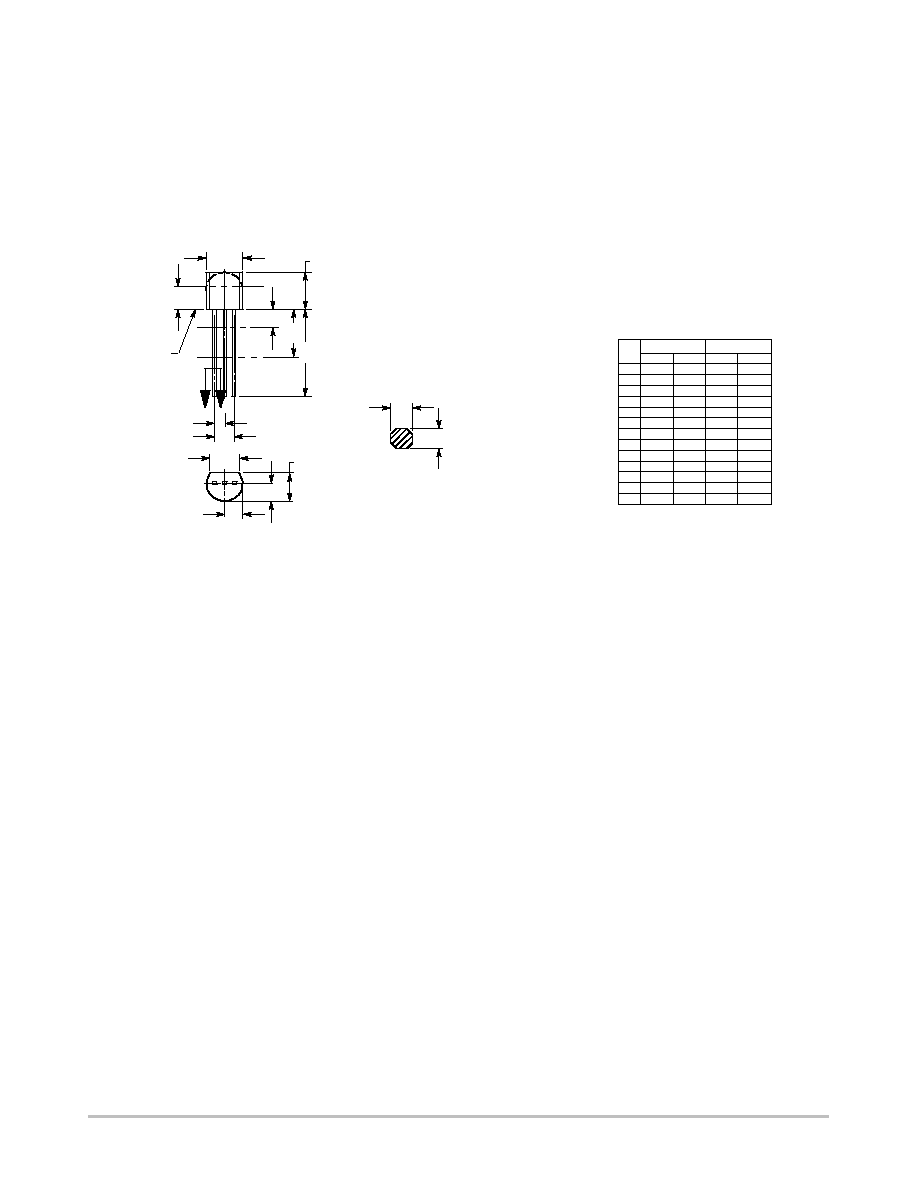
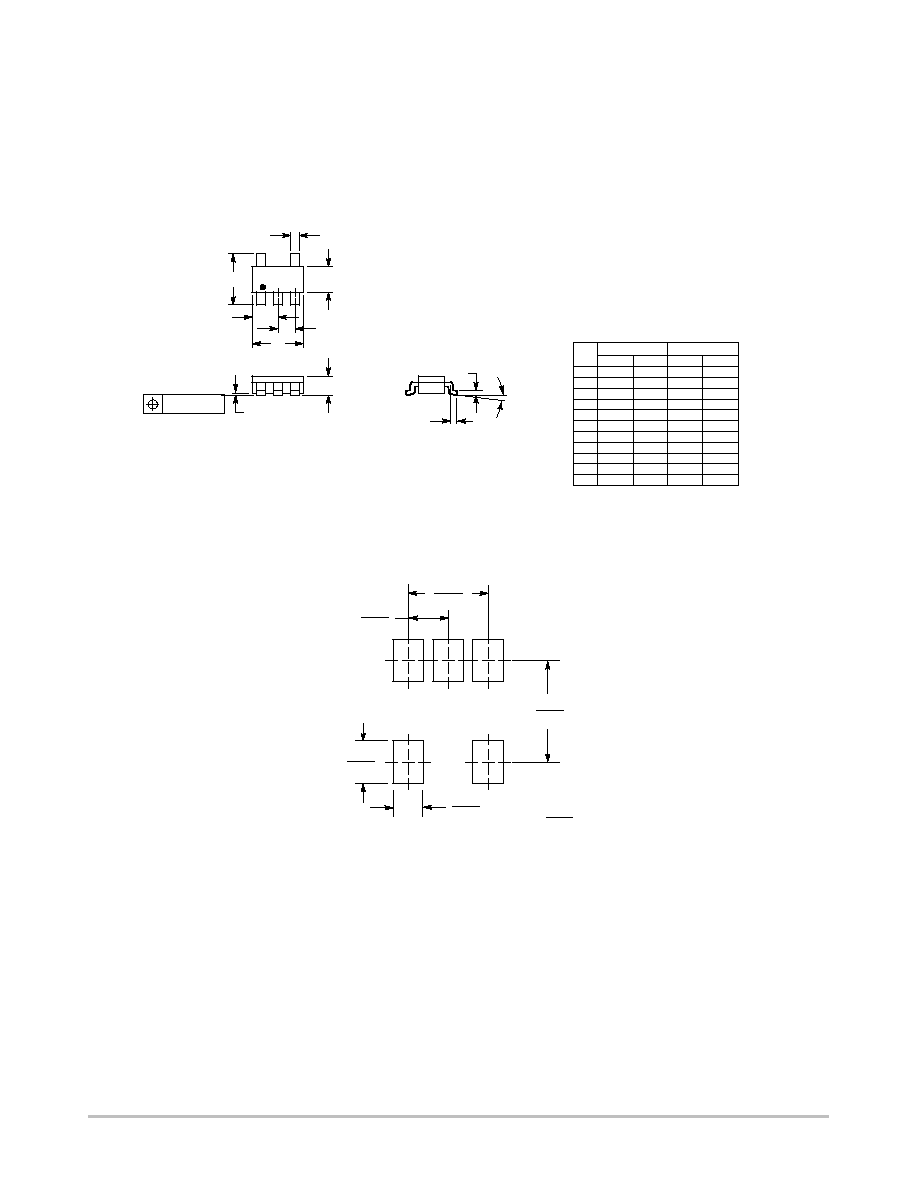
PACKAGE DIMENSIONS
P SUFFIX
PLASTIC PACKAGE
CASE 29-11
(TO-92)
ISSUE AL
NOTES:
1. DIMENSIONING AND TOLERANCING PER ANSI
Y14.5M, 1982.
2. CONTROLLING DIMENSION: INCH.
3. CONTOUR OF PACKAGE BEYOND DIMENSION R
IS UNCONTROLLED.
4. LEAD DIMENSION IS UNCONTROLLED IN P AND
BEYOND DIMENSION K MINIMUM.
R
A
P
J
L
B
K
G
H
SECTION X-X
C
V
D
N
N
X X
SEATING
PLANE
DIM
MIN
MAX
MIN
MAX
MILLIMETERS
INCHES
A
0.175
0.205
4.45
5.20
B
0.170
0.210
4.32
5.33
C
0.125
0.165
3.18
4.19
D
0.016
0.021
0.407
0.533
G
0.045
0.055
1.15
1.39
H
0.095
0.105
2.42
2.66
J
0.015
0.020
0.39
0.50
K
0.500
---
12.70
---
L
0.250
---
6.35
---
N
0.080
0.105
2.04
2.66
P
---
0.100
---
2.54
R
0.115
---
2.93
---
V
0.135
---
3.43
---
1
MC34064, MC33064, NCV33064
http://onsemi.com
9
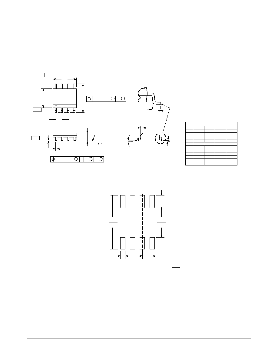
PACKAGE DIMENSIONS
SN SUFFIX
PLASTIC PACKAGE
CASE 483-02
ISSUE C
NOTES:
1. DIMENSIONING AND TOLERANCING PER
ANSI Y14.5M, 1982.
2. CONTROLLING DIMENSION: MILLIMETER.
3. MAXIMUM LEAD THICKNESS INCLUDES
LEAD FINISH THICKNESS. MINIMUM LEAD
THICKNESS IS THE MINIMUM THICKNESS
OF BASE MATERIAL.
4. A AND B DIMENSIONS DO NOT INCLUDE
MOLD FLASH, PROTRUSIONS, OR GATE
BURRS.
DIM
MIN
MAX
MIN
MAX
INCHES
MILLIMETERS
A
2.90
3.10 0.1142 0.1220
B
1.30
1.70 0.0512 0.0669
C
0.90
1.10 0.0354 0.0433
D
0.25
0.50 0.0098 0.0197
G
0.85
1.05 0.0335 0.0413
H
0.013
0.100 0.0005 0.0040
J
0.10
0.26 0.0040 0.0102
K
0.20
0.60 0.0079 0.0236
L
1.25
1.55 0.0493 0.0610
M
0
10
0
10
S
2.50
3.00 0.0985 0.1181
0.05 (0.002)
1
2
3
5
4
S
A
G
L
B
D
H
C
K
M
J
_
_
_
_
0.7
0.028
1.0
0.039
mm
inches
SCALE 10:1
0.95
0.037
2.4
0.094
1.9
0.074
SOLDERING FOOTPRINT
MC34064, MC33064, NCV33064
http://onsemi.com
10
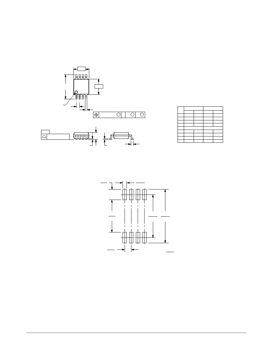
PACKAGE DIMENSIONS
D SUFFIX
PLASTIC PACKAGE
CASE 751-07
(SOIC-8 NB)
ISSUE AE
SEATING
PLANE
1
4
5
8
N
J
X 45
_
K
NOTES:
1. DIMENSIONING AND TOLERANCING PER
ANSI Y14.5M, 1982.
2. CONTROLLING DIMENSION: MILLIMETER.
3. DIMENSION A AND B DO NOT INCLUDE
MOLD PROTRUSION.
4. MAXIMUM MOLD PROTRUSION 0.15 (0.006)
PER SIDE.
5. DIMENSION D DOES NOT INCLUDE DAMBAR
PROTRUSION. ALLOWABLE DAMBAR
PROTRUSION SHALL BE 0.127 (0.005) TOTAL
IN EXCESS OF THE D DIMENSION AT
MAXIMUM MATERIAL CONDITION.
6. 751-01 THRU 751-06 ARE OBSOLETE. NEW
STANDARD IS 751-07.
A
B
S
D
H
C
0.10 (0.004)
DIM
A
MIN
MAX
MIN
MAX
INCHES
4.80
5.00
0.189
0.197
MILLIMETERS
B
3.80
4.00
0.150
0.157
C
1.35
1.75
0.053
0.069
D
0.33
0.51
0.013
0.020
G
1.27 BSC
0.050 BSC
H
0.10
0.25
0.004
0.010
J
0.19
0.25
0.007
0.010
K
0.40
1.27
0.016
0.050
M
0
8
0
8
N
0.25
0.50
0.010
0.020
S
5.80
6.20
0.228
0.244
-X-
-Y-
G
M
Y
M
0.25 (0.010)
-Z-
Y
M
0.25 (0.010)
Z
S
X
S
M
_
_
_
_
1.52
0.060
7.0
0.275
0.6
0.024
1.270
0.050
4.0
0.155
mm
inches
SCALE 6:1
*For additional information on our Pb-Free strategy and soldering
details, please download the ON Semiconductor Soldering and
Mounting Techniques Reference Manual, SOLDERRM/D.
SOLDERING FOOTPRINT*
MC34064, MC33064, NCV33064
http://onsemi.com
11
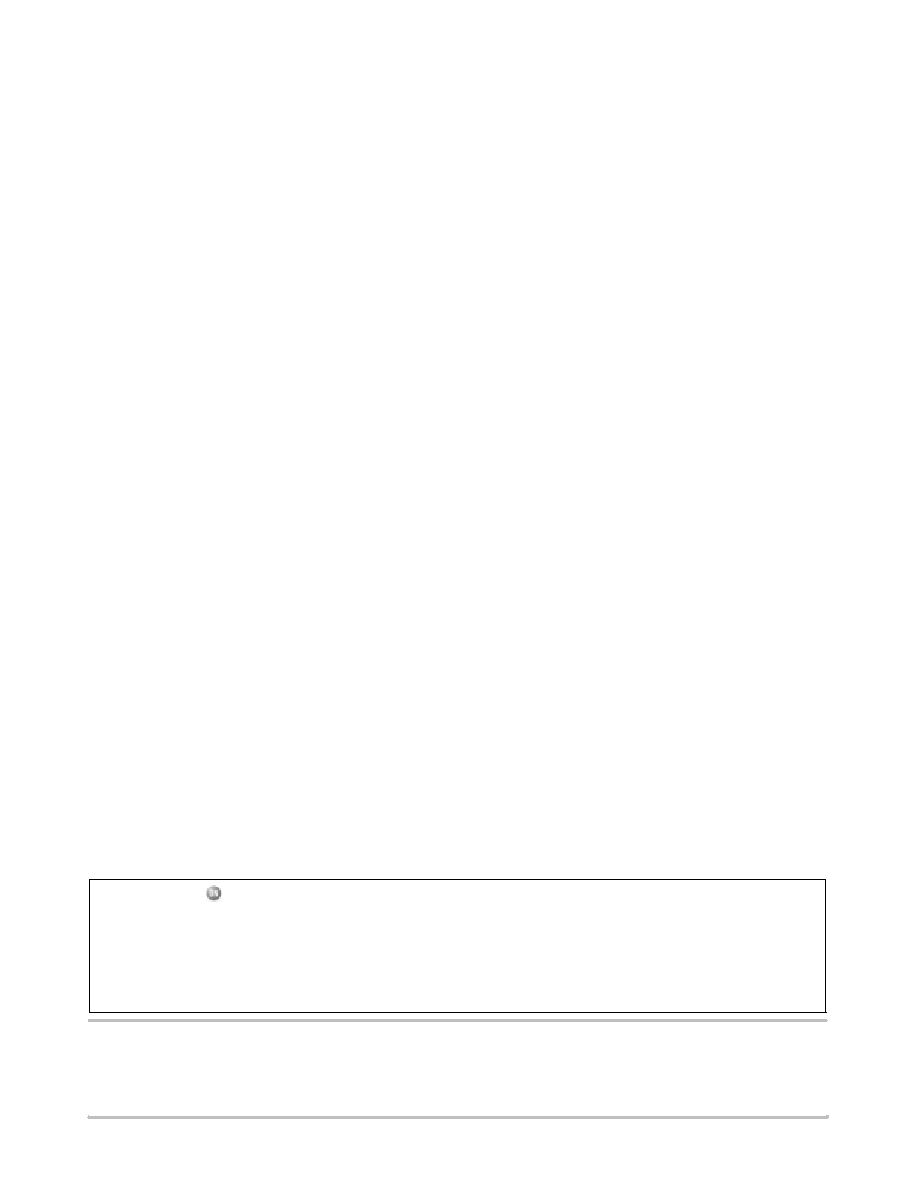
PACKAGE DIMENSIONS
S
B
M
0.08 (0.003)
A
S
T
DIM
MIN
MAX
MIN
MAX
INCHES
MILLIMETERS
A
2.90
3.10
0.114
0.122
B
2.90
3.10
0.114
0.122
C
---
1.10
---
0.043
D
0.25
0.40
0.010
0.016
G
0.65 BSC
0.026 BSC
H
0.05
0.15
0.002
0.006
J
0.13
0.23
0.005
0.009
K
4.75
5.05
0.187
0.199
L
0.40
0.70
0.016
0.028
NOTES:
1. DIMENSIONING AND TOLERANCING PER ANSI
Y14.5M, 1982.
2. CONTROLLING DIMENSION: MILLIMETER.
3. DIMENSION A DOES NOT INCLUDE MOLD FLASH,
PROTRUSIONS OR GATE BURRS. MOLD FLASH,
PROTRUSIONS OR GATE BURRS SHALL NOT
EXCEED 0.15 (0.006) PER SIDE.
4. DIMENSION B DOES NOT INCLUDE INTERLEAD
FLASH OR PROTRUSION. INTERLEAD FLASH OR
PROTRUSION SHALL NOT EXCEED 0.25 (0.010)
PER SIDE.
5. 846A-01 OBSOLETE, NEW STANDARD 846A-02.
-B-
-A-
D
K
G
PIN 1 ID
8 PL
0.038 (0.0015)
-T-
SEATING
PLANE
C
H
J
L
DM SUFFIX
PLASTIC PACKAGE
CASE 846A-02
(Micro8)
ISSUE F
8X
8X
6X
mm
inches
SCALE 8:1
1.04
0.041
0.38
0.015
5.28
0.208
4.24
0.167
3.20
0.126
0.65
0.0256
*For additional information on our Pb-Free strategy and soldering
details, please download the ON Semiconductor Soldering and
Mounting Techniques Reference Manual, SOLDERRM/D.
SOLDERING FOOTPRINT*
MC34064, MC33064, NCV33064
http://onsemi.com
12
ON Semiconductor and are registered trademarks of Semiconductor Components Industries, LLC (SCILLC). SCILLC reserves the right to make changes without further notice
to any products herein. SCILLC makes no warranty, representation or guarantee regarding the suitability of its products for any particular purpose, nor does SCILLC assume any liability
arising out of the application or use of any product or circuit, and specifically disclaims any and all liability, including without limitation special, consequential or incidental damages.
"Typical" parameters which may be provided in SCILLC data sheets and/or specifications can and do vary in different applications and actual performance may vary over time. All
operating parameters, including "Typicals" must be validated for each customer application by customer's technical experts. SCILLC does not convey any license under its patent rights
nor the rights of others. SCILLC products are not designed, intended, or authorized for use as components in systems intended for surgical implant into the body, or other applications
intended to support or sustain life, or for any other application in which the failure of the SCILLC product could create a situation where personal injury or death may occur. Should
Buyer purchase or use SCILLC products for any such unintended or unauthorized application, Buyer shall indemnify and hold SCILLC and its officers, employees, subsidiaries, affiliates,
and distributors harmless against all claims, costs, damages, and expenses, and reasonable attorney fees arising out of, directly or indirectly, any claim of personal injury or death
associated with such unintended or unauthorized use, even if such claim alleges that SCILLC was negligent regarding the design or manufacture of the part. SCILLC is an Equal
Opportunity/Affirmative Action Employer. This literature is subject to all applicable copyright laws and is not for resale in any manner.
PUBLICATION ORDERING INFORMATION
N. American Technical Support: 800-282-9855 Toll Free
USA/Canada
Japan: ON Semiconductor, Japan Customer Focus Center
2-9-1 Kamimeguro, Meguro-ku, Tokyo, Japan 153-0051
Phone: 81-3-5773-3850
MC34064/D
Micro8 is a trademark of International Rectifier.
LITERATURE FULFILLMENT:
Literature Distribution Center for ON Semiconductor
P.O. Box 61312, Phoenix, Arizona 85082-1312 USA
Phone: 480-829-7710 or 800-344-3860 Toll Free USA/Canada
Fax: 480-829-7709 or 800-344-3867 Toll Free USA/Canada
Email: orderlit@onsemi.com
ON Semiconductor Website: http://onsemi.com
Order Literature: http://www.onsemi.com/litorder
For additional information, please contact your
local Sales Representative.