
©
Semiconductor Components Industries, LLC, 2002
June, 2002 ≠ Rev. 6
1
Publication Order Number:
MC74AC10/D
MC74AC10, MC74ACT10
Triple 3-Input NAND Gate
∑
Outputs Source/Sink 24 mA
∑
ACT10 Has TTL Compatible Inputs
13
14
12
11
10
9
8
2
1
3
4
5
6
7
GND
V
CC
Figure 1. Pinout: 14≠Lead Packages Conductors
(Top View)
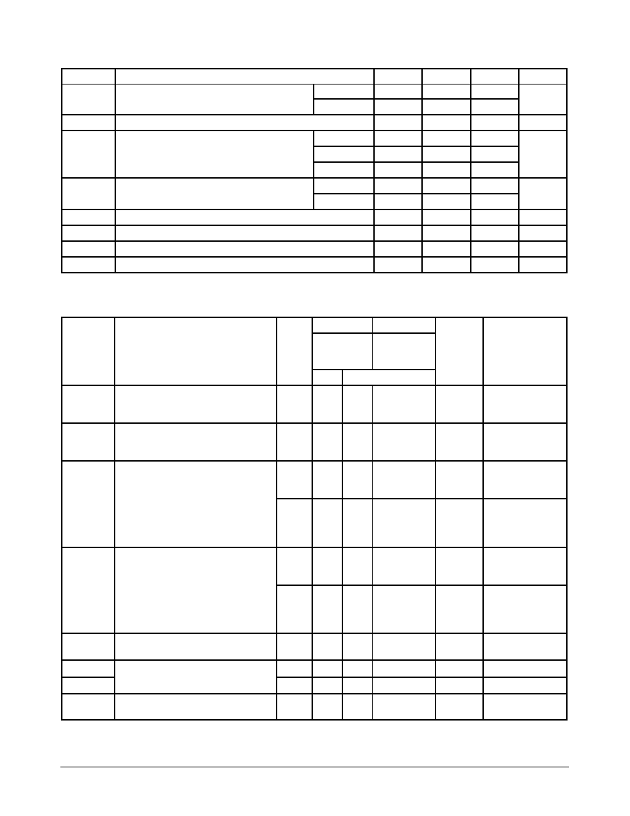
MAXIMUM RATINGS*
Rating
Symbol
Value
Unit
DC Supply Voltage (Referenced to GND)
V
CC
≠0.5 to
+7.0
V
DC Input Voltage (Referenced to GND)
V
in
≠0.5 to
V
CC
+0.5
V
DC Output Voltage (Referenced to GND)
V
out
≠0.5 to
V
CC
+0.5
V
DC Input Current, per Pin
I
in
±
20
mA
DC Output Sink/Source Current, per Pin
I
out
±
50
mA
DC V
CC
or GND Current per Output Pin
I
CC
±
50
mA
Storage Temperature
T
stg
≠65 to
+150
∞
C
*Maximum Ratings are those values beyond which damage to the device may
occur. Functional operation should be restricted to the Recommended
Operating Conditions.
TSSOP≠14
DT SUFFIX
CASE 948G
1
14
EIAJ≠14
M SUFFIX
CASE 965
1
14
SO≠14
D SUFFIX
CASE 751A
1
14
1
14
PDIP≠14
N SUFFIX
CASE 646
Device
Package
Shipping
ORDERING INFORMATION
MC74AC10DT
TSSOP≠14
96 Units/Rail
MC74AC10DTR2
TSSOP≠14 2500 Tape & Reel
MC74ACT10DT
TSSOP≠14
96 Units/Rail
MC74ACT10DTR2
TSSOP≠14 2500 Tape & Reel
MC74AC10N
PDIP≠14
25 Units/Rail
MC74AC10D
SOIC≠14
55 Units/Rail
MC74ACT10N
PDIP≠14
25 Units/Rail
MC74AC10DR2
SOIC≠14
2500 Tape & Reel
MC74ACT10D
SOIC≠14
55 Units/Rail
MC74ACT10DR2
SOIC≠14
2500 Tape & Reel
MC74AC10M
EIAJ≠14
50 Units/Rail
MC74ACT10M
EIAJ≠14
50 Units/Rail
MC74ACT10MEL
EIAJ≠14
2000 Tape & Reel
See general marking information in the device marking
section on page 5 of this data sheet.
DEVICE MARKING INFORMATION
http://onsemi.com
MC74AC10, MC74ACT10
http://onsemi.com
2
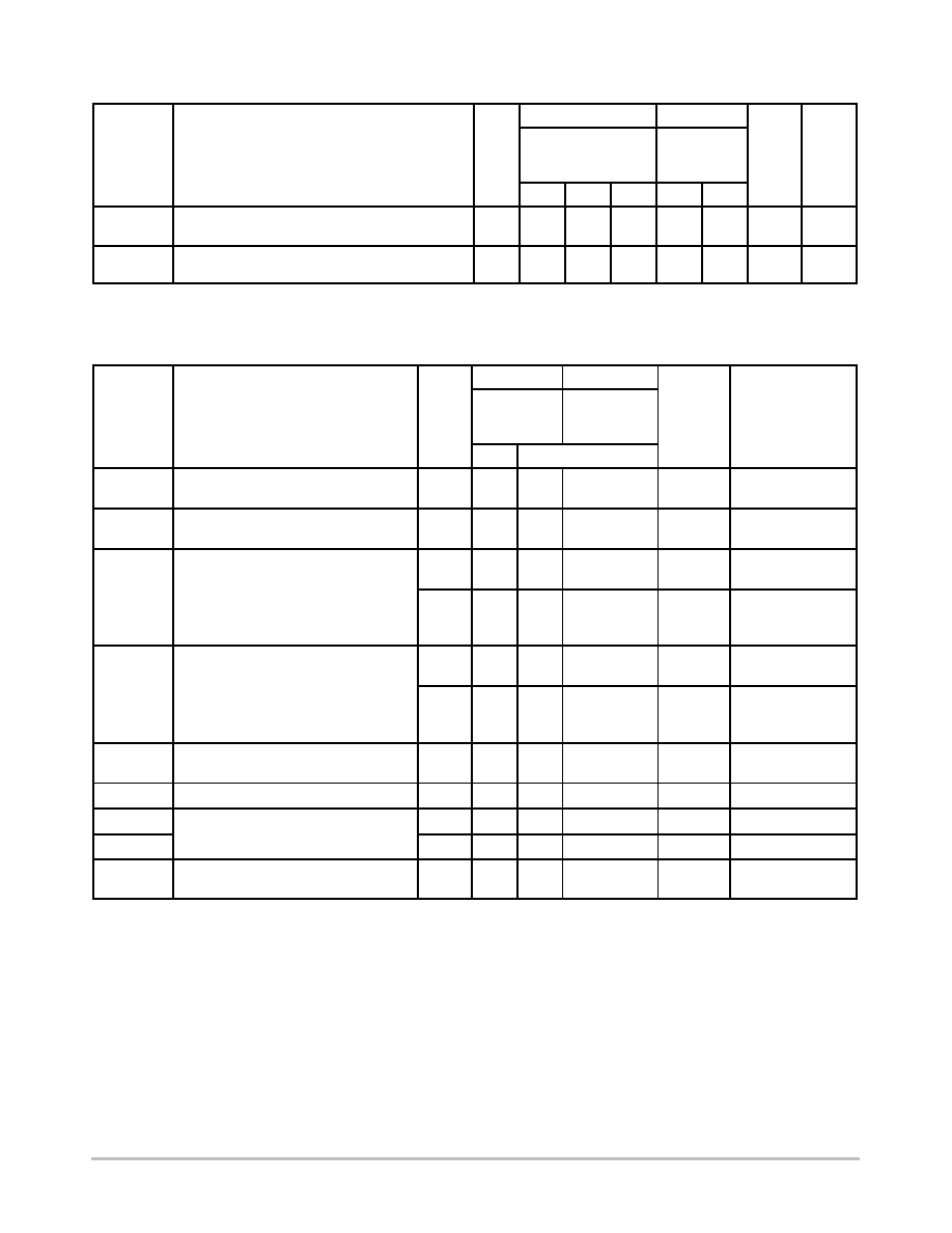
RECOMMENDED OPERATING CONDITIONS
Symbol
Parameter
Min
Typ
Max
Unit
V
Supply Voltage
AC
2.0
5.0
6.0
V
V
CC
Supply Voltage
ACT
4.5
5.0
5.5
V
V
in
, V
out
DC Input Voltage, Output Voltage (Ref. to GND)
0
≠
V
CC
V
V
CC
@ 3.0 V
≠
150
≠
t
r
, t
f
Input Rise and Fall Time (Note 1)
AC Devices except Schmitt Inputs
V
CC
@ 4.5 V
≠
40
≠
ns/V
r
,
f
AC Devices except Schmitt Inputs
V
CC
@ 5.5 V
≠
25
≠
t t
Input Rise and Fall Time (Note 2)
V
CC
@ 4.5 V
≠
10
≠
ns/V
t
r
, t
f
In ut Rise and Fall Time (Note 2)
ACT Devices except Schmitt Inputs
V
CC
@ 5.5 V
≠
8.0
≠
ns/V
T
J
Junction Temperature (PDIP)
≠
≠
140
∞
C
T
A
Operating Ambient Temperature Range
≠40
25
85
∞
C
I
OH
Output Current ≠ High
≠
≠
≠24
mA
I
OL
Output Current ≠ Low
≠
≠
24
mA
1. V
in
from 30% to 70% V
CC
; see individual Data Sheets for devices that differ from the typical input rise and fall times.
2. V
in
from 0.8 V to 2.0 V; see individual Data Sheets for devices that differ from the typical input rise and fall times.
DC CHARACTERISTICS
74AC
74AC
Symbol
Parameter
V
CC
(V)
T
A
= +25
∞
C
T
A
=
≠40
∞
C to
+85
∞
C
Unit
Conditions
Typ
Guaranteed Limits
V
IH
Minimum High Level
3.0
1.5
2.1
2.1
V
OUT
= 0.1 V
u
g
e e
Input Voltage
4.5
2.25
3.15
3.15
V
or V
CC
≠ 0.1 V
5.5
2.75
3.85
3.85
V
IL
Maximum Low Level
3.0
1.5
0.9
0.9
V
OUT
= 0.1 V
a
u
o
e e
Input Voltage
4.5
2.25
1.35
1.35
V
or V
CC
≠ 0.1 V
5.5
2.75
1.65
1.65
V
OH
Minimum High Level
3.0
2.99
2.9
2.9
I
OUT
= ≠50
µ
A
u
g
e e
Output Voltage
4.5
4.49
4.4
4.4
V
5.5
5.49
5.4
5.4
*V
IN
= V
IL
or V
IH
3.0
≠
2.56
2.46
V
≠12 mA
4.5
≠
3.86
3.76
V
I
OH
≠24 mA
5.5
≠
4.86
4.76
≠24 mA
V
OL
Maximum Low Level
3.0
0.002
0.1
0.1
I
OUT
= 50
µ
A
a
u
o
e e
Output Voltage
4.5
0.001
0.1
0.1
V
5.5
0.001
0.1
0.1
*V
IN
= V
IL
or V
IH
3.0
≠
0.36
0.44
V
12 mA
4.5
≠
0.36
0.44
V
I
OL
24 mA
5.5
≠
0.36
0.44
24 mA
I
IN
Maximum Input
5 5
≠
±
0 1
±
1 0
µ
A
V
I
= V
CC
GND
a
u
u
Leakage Current
5.5
≠
±
0.1
±
1.0
µ
A
V
I
= V
CC
, GND
I
OLD
Minimum Dynamic
O t
t C
t
5.5
≠
≠
75
mA
V
OLD
= 1.65 V Max
I
OHD
Output Current
5.5
≠
≠
≠75
mA
V
OHD
= 3.85 V Min
I
CC
Maximum Quiescent
5 5
≠
4 0
40
µ
A
V
IN
= V
CC
or GND
a
u
Qu esce
Supply Current
5.5
≠
4.0
40
µ
A
V
IN
= V
CC
or GND
*All outputs loaded; thresholds on input associated with output under test.
Maximum test duration 2.0 ms, one output loaded at a time.
NOTE:
I
IN
and I
CC
@ 3.0 V are guaranteed to be less than or equal to the respective limit @ 5.5 V V
CC
.
MC74AC10, MC74ACT10
http://onsemi.com
3
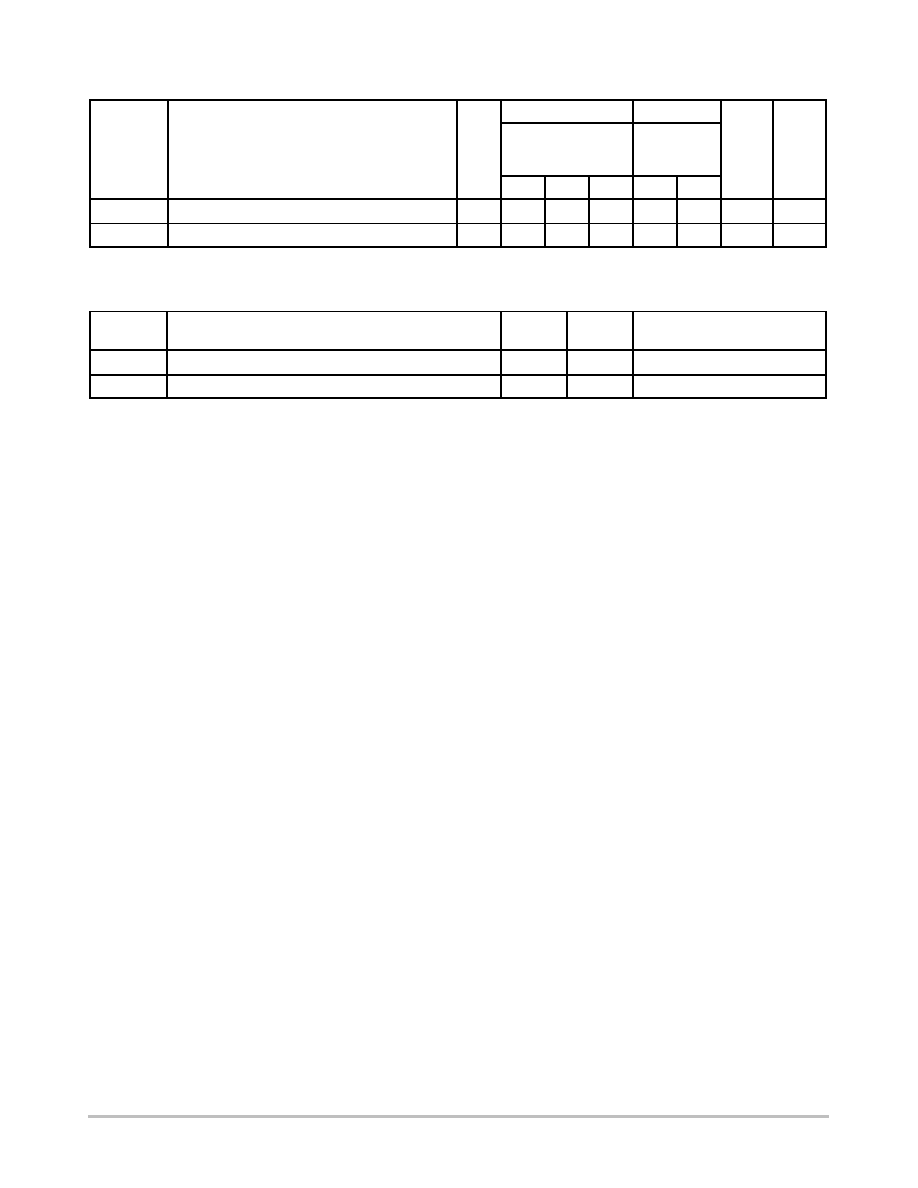
AC CHARACTERISTICS
(For Figures and Waveforms ≠ See Section 3 of the ON Semiconductor FACT Data Book, DL138/D)
74AC
74AC
Symbol
Parameter
V
CC
*
(V)
T
A
= +25
∞
C
C
L
= 50 pF
T
A
= ≠40
∞
C
to +85
∞
C
C
L
= 50 pF
Unit
Fig.
No.
Min
Typ
Max
Min
Max
t
PLH
Propagation Delay
3.3
1.5
6.0
9.5
1.0
10.5
ns
3≠5
t
PLH
Propagation Delay
5.0
1.5
4.5
7.0
1.0
8.0
ns
3≠5
t
PHL
Propagation Delay
3.3
1.5
5.5
8.5
1.0
10.0
ns
3≠5
t
PHL
Propagation Delay
5.0
1.5
4.0
6.0
1.0
6.5
ns
3≠5
*Voltage Range 3.3 V is 3.3 V
±
0.3 V.
Voltage Range 5.0 V is 5.0 V
±
0.5 V.
DC CHARACTERISTICS
74ACT
74ACT
Symbol
Parameter
V
CC
(V)
T
A
= +25
∞
C
T
A
=
≠40
∞
C to
+85
∞
C
Unit
Conditions
Typ
Guaranteed Limits
V
IH
Minimum High Level
4.5
1.5
2.0
2.0
V
V
OUT
= 0.1 V
u
g
e e
Input Voltage
5.5
1.5
2.0
2.0
V
or V
CC
≠ 0.1 V
V
IL
Maximum Low Level
4.5
1.5
0.8
0.8
V
V
OUT
= 0.1 V
a
u
o
e e
Input Voltage
5.5
1.5
0.8
0.8
V
or V
CC
≠ 0.1 V
V
OH
Minimum High Level
4.5
4.49
4.4
4.4
V
I
OUT
= ≠50
µ
A
u
g
e e
Output Voltage
5.5
5.49
5.4
5.4
V
*V
IN
= V
IL
or V
IH
4.5
≠
3.86
3.76
V
I
OH
≠24 mA
5.5
≠
4.86
4.76
I
OH
≠24 mA
V
OL
Maximum Low Level
4.5
0.001
0.1
0.1
V
I
OUT
= 50
µ
A
a
u
o
e e
Output Voltage
5.5
0.001
0.1
0.1
V
*V
IN
= V
IL
or V
IH
4.5
≠
0.36
0.44
V
I
OL
24 mA
5.5
≠
0.36
0.44
I
OL
24 mA
I
IN
Maximum Input
5 5
≠
±
0 1
±
1 0
µ
A
V
I
= V
CC
GND
a
u
u
Leakage Current
5.5
≠
±
0.1
±
1.0
µ
A
V
I
= V
CC
, GND
I
CCT
Additional Max. I
CC
/Input
5.5
0.6
≠
1.5
mA
V
I
= V
CC
≠ 2.1 V
I
OLD
Minimum Dynamic
O t
t C
t
5.5
≠
≠
75
mA
V
OLD
= 1.65 V Max
I
OHD
Output Current
5.5
≠
≠
≠75
mA
V
OHD
= 3.85 V Min
I
CC
Maximum Quiescent
5 5
≠
4 0
40
µ
A
V
IN
= V
CC
or GND
a
u
Qu esce
Supply Current
5.5
≠
4.0
40
µ
A
V
IN
= V
CC
or GND
*All outputs loaded; thresholds on input associated with output under test.
Maximum test duration 2.0 ms, one output loaded at a time.
MC74AC10, MC74ACT10
http://onsemi.com
4
AC CHARACTERISTICS
(For Figures and Waveforms ≠ See Section 3 of the ON Semiconductor FACT Data Book, DL138/D)
74ACT
74ACT
Symbol
Parameter
V
CC
*
(V)
T
A
= +25
∞
C
C
L
= 50 pF
T
A
= ≠40
∞
C
to +85
∞
C
C
L
= 50 pF
Unit
Fig.
No.
Min
Typ
Max
Min
Max
t
PLH
Propagation Delay
5.0
1.0
≠
9.0
1.0
10.0
ns
3≠5
t
PHL
Propagation Delay
5.0
1.0
≠
9.0
1.0
9.5
ns
3≠5
*Voltage Range 5.0 V is 5.0 V
±
0.5 V.
CAPACITANCE
Symbol
Parameter
Value
Typ
Unit
Test Conditions
C
IN
Input Capacitance
4.5
pF
V
CC
= 5.0 V
C
PD
Power Dissipation Capacitance
25
pF
V
CC
= 5.0 V
MC74AC10, MC74ACT10
http://onsemi.com
5
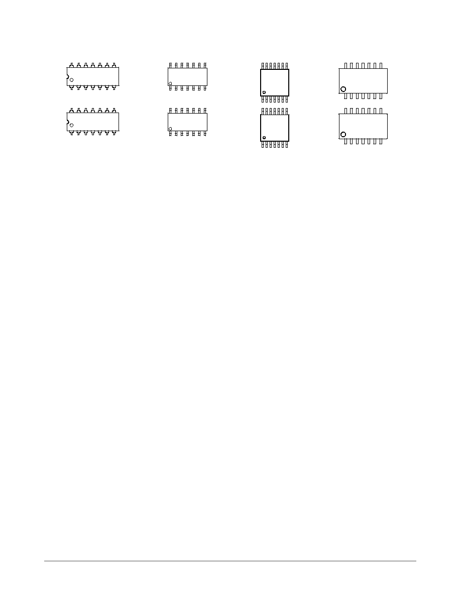
MARKING DIAGRAMS
A
= Assembly Location
WL, L
= Wafer Lot
YY, Y
= Year
WW, W = Work Week
PDIP≠14
SO≠14
TSSOP≠14
MC74AC10N
AWLYYWW
AC10
AWLYWW
AC
10
ALYW
ACT
10
ALYW
ACT10
AWLYWW
MC74ACT10N
AWLYYWW
74AC10
ALYW
EIAJ≠14
74ACT10
ALYW