Äîêóìåíòàöèÿ è îïèñàíèÿ www.docs.chipfind.ru
©
Semiconductor Components Industries, LLC, 2001
May, 2001 Rev. 6
1
Publication Order Number:
MC74AC574/D
MC74AC574, MC74ACT574
Octal D Flip-Flop with
3-State Outputs
The MC74AC574/74ACT574 is a highspeed, low power octal
flipflop with a buffered common Clock (CP) and a buffered common
Output Enable (OE). The information presented to the D inputs is
stored in the flipflops on the LOWtoHIGH
Clock (CP) transition.
The MC74AC574/74ACT574 is functionally identical to the
MC74AC374/74ACT374 except for the pinouts.
·
Inputs and Outputs on Opposite Sides of Package
Allowing Easy Interface with Microprocessors
·
Useful as Input or Output Port for Microprocessors
·
Functionally Identical to MC74AC374/74ACT374
·
3-State Outputs for Bus-Oriented Applications
·
Outputs Source/Sink 24 mA
·
ACT574 Has TTL Compatible Inputs
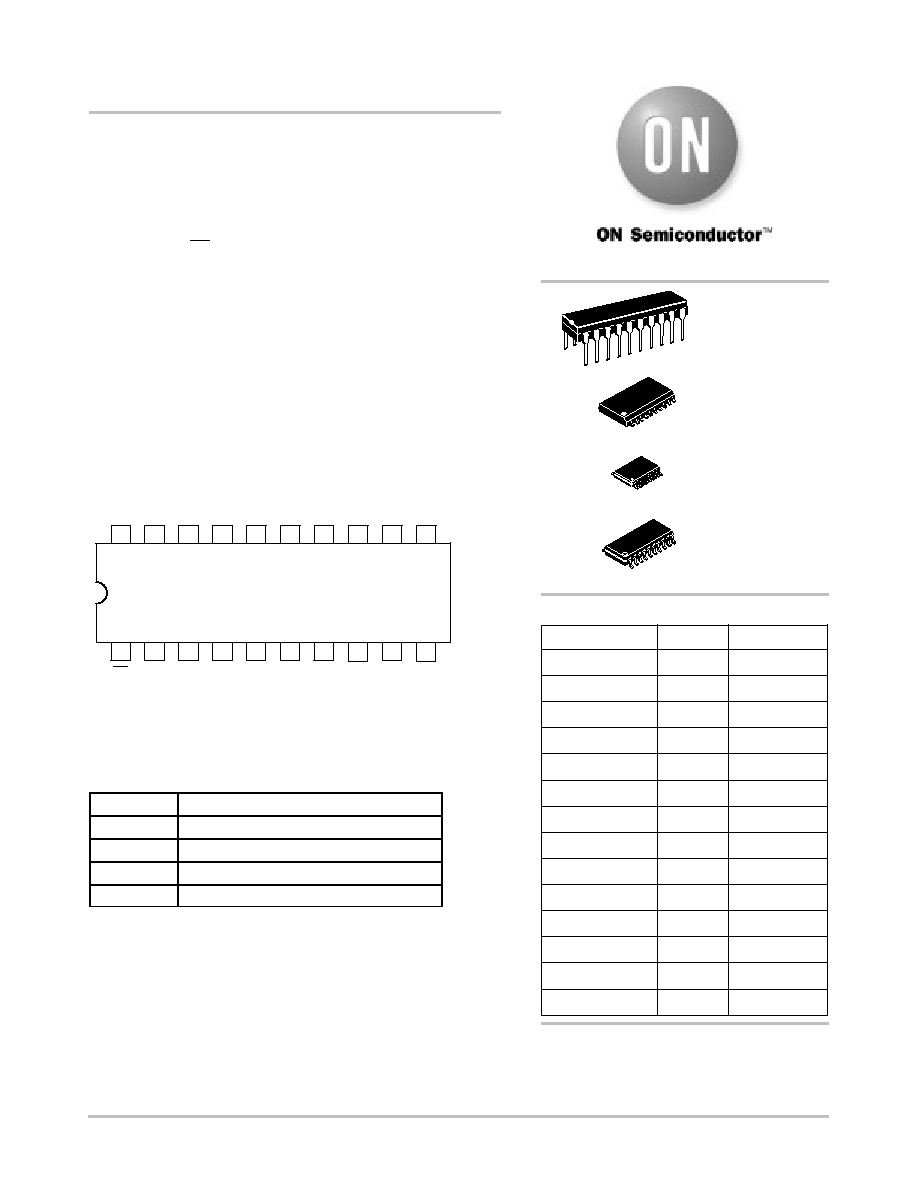
Figure 1. Pinout: 20Lead Packages Conductors
(Top View)
19
20
18
17
16
15
14
2
1
3
4
5
6
7
VCC
13
8
12
9
11
10
O0
O1
O2
O3
O4
O5
O6
O7
CP
OE
D0
D1
D2
D3
D4
D5
D6
D7 GND
PIN ASSIGNMENT
PIN
FUNCTION
D0D7
Data Inputs
CP
Clock Pulse Input
OE
3State Output Enable Input
O0O7
3State Outputs
http://onsemi.com
1
20
PDIP20
N SUFFIX
CASE 738
1
20
1
20
1
20
SO20
DW SUFFIX
CASE 751
TSSOP20
DT SUFFIX
CASE 948E
EIAJ20
M SUFFIX
CASE 967
Device
Package
Shipping
ORDERING INFORMATION
MC74AC574N
PDIP20
18 Units/Rail
MC74ACT574N
PDIP20
18 Units/Rail
MC74AC574DW
SOIC20
38 Units/Rail
MC74AC574DWR2
SOIC20
1000 Tape & Reel
MC74ACT574DW
SOIC20
38 Units/Rail
MC74ACT574DWR2
SOIC20
1000 Tape & Reel
MC74AC574DT
TSSOP20
75 Units/Rail
MC74AC574DTR2
TSSOP20
2500 Tape & Reel
MC74ACT574DT
TSSOP20
75 Units/Rail
MC74ACT574DTR2
TSSOP20
2500 Tape & Reel
MC74AC574M
EIAJ20
40 Units/Rail
MC74AC574MEL
EIAJ20
2000 Tape & Reel
MC74ACT574M
EIAJ20
40 Units/Rail
MC74ACT574MEL
EIAJ20
2000 Tape & Reel
See general marking information in the device marking
section on page 8 of this data sheet.
DEVICE MARKING INFORMATION
MC74AC574, MC74ACT574
http://onsemi.com
2
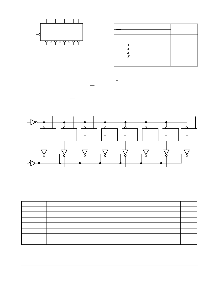
Figure 2. Logic Symbol
O0 O1 O2 O3 O4 O5 O6 O7
D0 D1 D2 D3 D4 D5 D6 D7
CP
OE
FUNCTIONAL DESCRIPTION
The MC74AC574/74ACT574 consists of eight edge-
triggered flipflops with individual Dtype inputs and
3state true outputs. The buffered clock and buffered Output
Enable are common to all flipflops. The eight flipflops
will store the state of their individual D inputs that meet the
setup and hold time requirements on the LOWtoHIGH
Clock (CP) transition. With the Output Enable (OE) LOW,
the contents of the eight flipflops are available at the
outputs. When OE is HIGH, the outputs go to the high
impedance state. Operation of the OE input does not affect
the state of the flipflops.
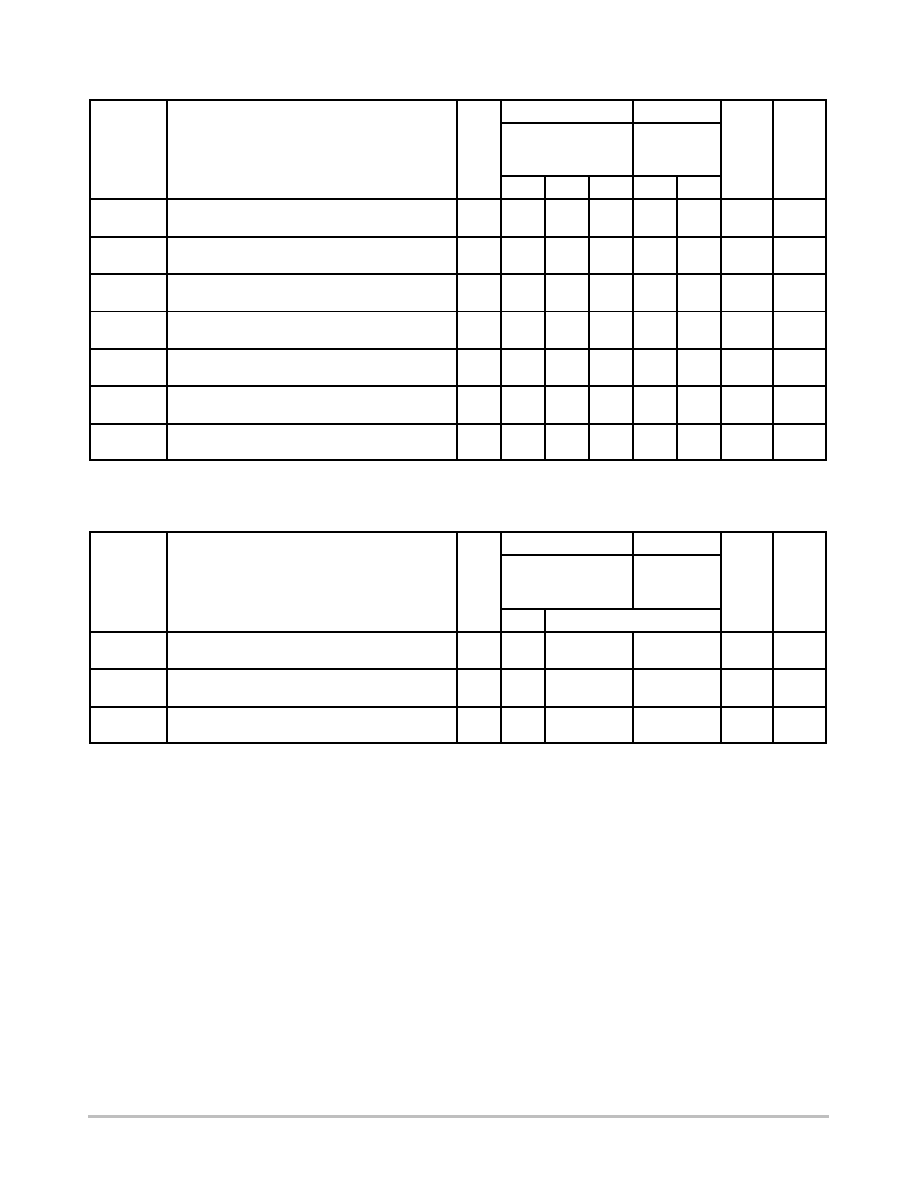
FUNCTION TABLE
Inputs
Internal
Outputs
F nction
OE
CP
D
Q
On
Function
H
H
L
NC
Z
Hold
H
H
H
NC
Z
Hold
H
L
L
Z
Load
H
H
H
Z
Load
L
L
L
L
Data Available
L
H
H
H
Data Available
L
H
L
NC
NC
No Change in Data
L
H
H
NC
NC
No Change in Data
H = HIGH Voltage Level
L = LOW Voltage Level
X = Immaterial
Z = High Impedance
= LOW-to-HIGH Clock Transition
NC = No Change
Figure 3. Logic Diagram
D0
D1
D2
D3
D4
D5
D6
D7
C
D
Q
O0
O1
O2
O3
O4
O5
O6
O7
OE
CP
C
D
Q
C
D
Q
C
D
Q
C
D
Q
C
D
Q
C
D
Q
C
D
Q
NOTE:
This diagram is provided only for the understanding of logic operations
and should not be used to estimate propagation delays.
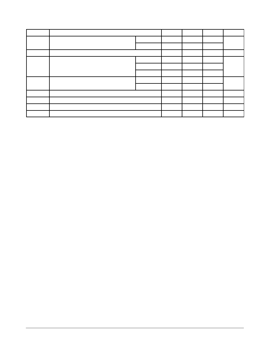
MAXIMUM RATINGS*
Symbol
Parameter
Value
Unit
VCC
DC Supply Voltage (Referenced to GND)
0.5 to +7.0
V
VIN
DC Input Voltage (Referenced to GND)
0.5 to VCC +0.5
V
VOUT
DC Output Voltage (Referenced to GND)
0.5 to VCC +0.5
V
IIN
DC Input Current, per Pin
±
20
mA
IOUT
DC Output Sink/Source Current, per Pin
±
50
mA
ICC
DC VCC or GND Current per Output Pin
±
50
mA
Tstg
Storage Temperature
65 to +150
°
C
* Maximum Ratings are those values beyond which damage to the device may occur. Functional operation should be restricted to the
Recommended Operating Conditions.
MC74AC574, MC74ACT574
http://onsemi.com
3
RECOMMENDED OPERATING CONDITIONS
Symbol
Parameter
Min
Typ
Max
Unit
VCC
Supply Voltage
AC
2.0
5.0
6.0
V
VCC
Supply Voltage
ACT
4.5
5.0
5.5
V
VIN, VOUT
DC Input Voltage, Output Voltage (Ref. to GND)
0
VCC
V
VCC @ 3.0 V
150
tr, tf
Input Rise and Fall Time (Note 1)
AC Devices except Schmitt Inputs
VCC @ 4.5 V
40
ns/V
r, f
AC Devices except Schmitt Inputs
VCC @ 5.5 V
25
t tf
Input Rise and Fall Time (Note 2)
VCC @ 4.5 V
10
ns/V
tr, tf
In ut Rise and Fall Time (Note 2)
ACT Devices except Schmitt Inputs
VCC @ 5.5 V
8.0
ns/V
TJ
Junction Temperature (PDIP)
140
°
C
TA
Operating Ambient Temperature Range
40
25
85
°
C
IOH
Output Current High
24
mA
IOL
Output Current Low
24
mA
1. VIN from 30% to 70% VCC; see individual Data Sheets for devices that differ from the typical input rise and fall times.
2. VIN from 0.8 V to 2.0 V; see individual Data Sheets for devices that differ from the typical input rise and fall times.
MC74AC574, MC74ACT574
http://onsemi.com
4
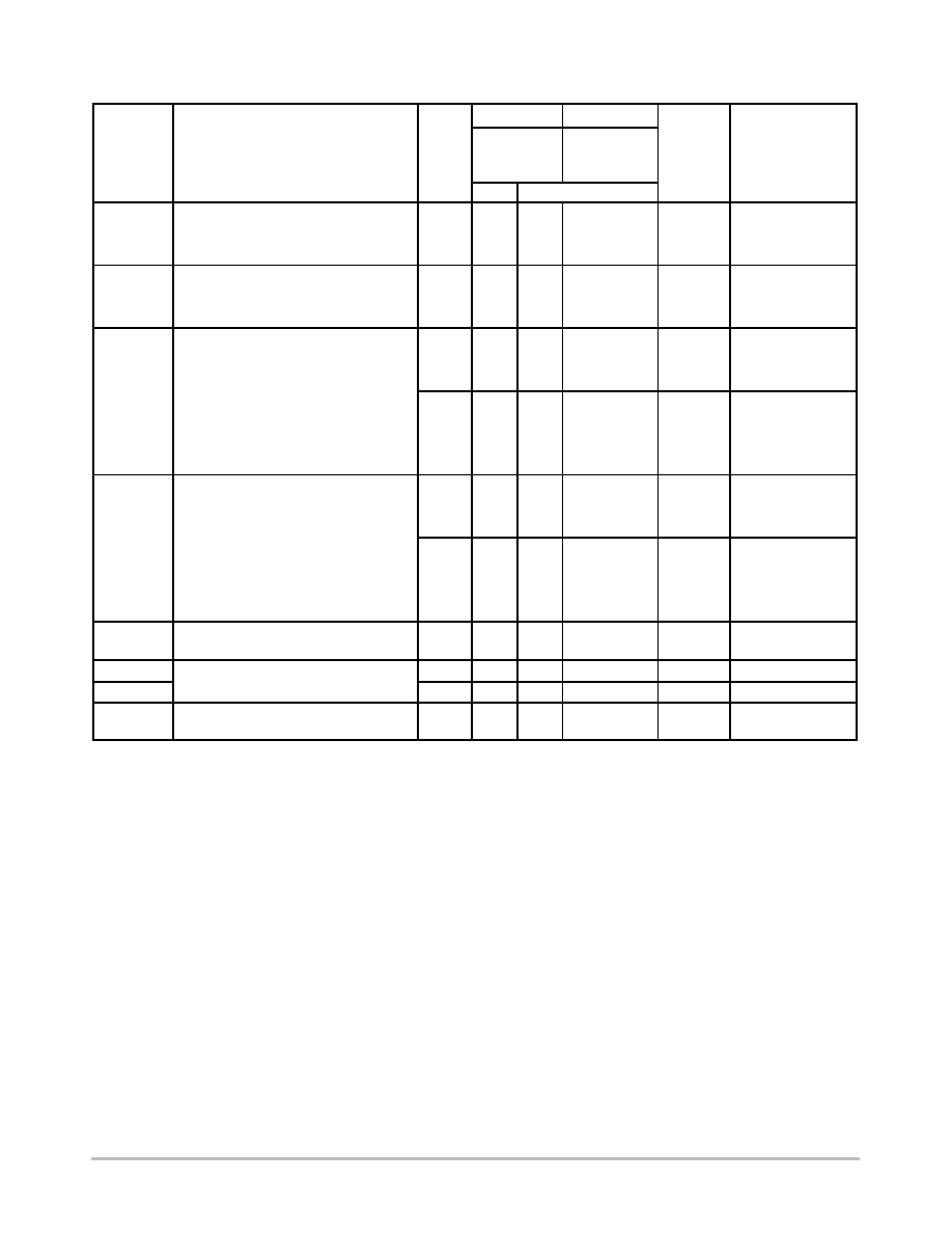
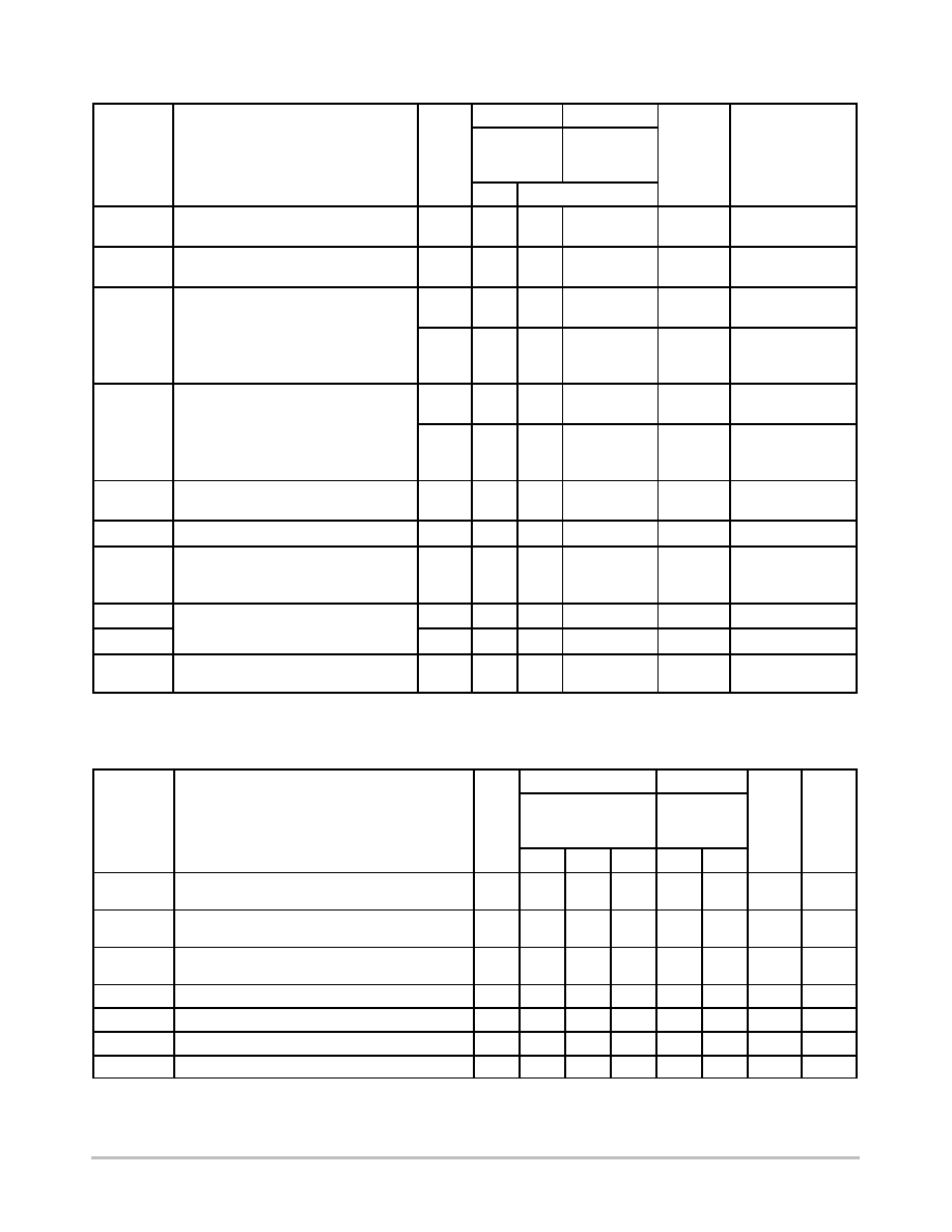
DC CHARACTERISTICS
74AC
74AC
Symbol
Parameter
VCC
(V)
TA = +25
°
C
TA =
40
°
C to
+85
°
C
Unit
Conditions
Typ
Guaranteed Limits
VIH
Minimum High Level
I
V l
3.0
1.5
2.1
2.1
VOUT = 0.1 V
g
Input Voltage
4.5
2.25
3.15
3.15
V
or VCC 0.1 V
5.5
2.75
3.85
3.85
VIL
Maximum Low Level
I
V l
3.0
1.5
0.9
0.9
VOUT = 0.1 V
Input Voltage
4.5
2.25
1.35
1.35
V
or VCC 0.1 V
5.5
2.75
1.65
1.65
VOH
Minimum High Level
O
V l
3.0
2.99
2.9
2.9
IOUT = 50
µ
A
g
Output Voltage
4.5
4.49
4.4
4.4
V
5.5
5.49
5.4
5.4
*VIN = VIL or VIH
3.0
2.56
2.46
V
12 mA
4.5
3.86
3.76
V
IOH
24 mA
5.5
4.86
4.76
24 mA
VOL
Maximum Low Level
O
V l
3.0
0.002
0.1
0.1
IOUT = 50
µ
A
Output Voltage
4.5
0.001
0.1
0.1
V
5.5
0.001
0.1
0.1
*VIN = VIL or VIH
3.0
0.36
0.44
V
12 mA
4.5
0.36
0.44
V
IOL
24 mA
5.5
0.36
0.44
24 mA
IIN
Maximum Input
5 5
±
0 1
±
1 0
µ
A
VI = VCC GND
IN
a
u
u
Leakage Current
5.5
±
0.1
±
1.0
µ
A
VI = VCC, GND
IOLD
Minimum Dynamic
5.5
75
mA
VOLD = 1.65 V Max
IOHD
y
Output Current
5.5
75
mA
VOHD = 3.85 V Min
ICC
Maximum Quiescent
5 5
8 0
80
µ
A
VIN VCC or GND
CC
a
u
Qu esce
Supply Current
5.5
8.0
80
µ
A
VIN = VCC or GND
* All outputs loaded; thresholds on input associated with output under test.
Maximum test duration 2.0 ms, one output loaded at a time.
NOTE:
Note: IIN and ICC @ 3.0 V are guaranteed to be less than or equal to the respective limit @ 5.5 V VCC.
MC74AC574, MC74ACT574
http://onsemi.com
5
AC CHARACTERISTICS (For Figures and Waveforms -- See Section 3)
74AC
74AC
Symbol
Parameter
VCC*
(V)
TA = +25
°
C
CL = 50 pF
TA = 40
°
C
to +85
°
C
CL = 50 pF
Unit
Fig.
No.
Min
Typ
Max
Min
Max
fmax
Maximum Clock
3.3
75
60
MHz
33
fmax
Frequency
5.0
95
85
MHz
33
tPLH
Propagation Delay
3.3
3.5
13.5
3.5
15
ns
36
tPLH
CP to On
5.0
2.0
9.5
2.0
11
ns
36
tPHL
Propagation Delay
3.3
3.5
12
3.5
13.5
ns
36
tPHL
CP to On
5.0
2.0
8.5
2.0
9.5
ns
36
tPZH
Output Enable Time
3.3
2.5
11
2.5
12
ns
37
tPZH
Output Enable Time
5.0
2.0
8.5
2.0
9.0
ns
37
tPZL
Output Enable Time
3.3
3.0
10.5
3.5
11.5
ns
38
tPZL
Output Enable Time
5.0
1.5
8.0
2.0
9.0
ns
38
tPHZ
Output Disable Time
3.3
4.0
12
4.5
13
ns
37
tPHZ
Output Disable Time
5.0
2.0
9.5
2.0
10.5
ns
37
tPLZ
Output Disable Time
3.3
2.0
9.0
2.5
10
ns
38
tPLZ
Output Disable Time
5.0
1.5
7.5
1.5
8.5
ns
38
* Voltage Range 3.3 V is 3.3 V
±
0.3 V.
Voltage Range 5.0 V is 5.0 V
±
0.5 V.
AC OPERATING REQUIREMENTS
74AC
74AC
Symbol
Parameter
VCC*
(V)
TA = +25
°
C
CL = 50 pF
TA = 40
°
C
to +85
°
C
CL = 50 pF
Unit
Fig.
No.
Typ
Guaranteed Minimum
ts
Setup Time, HIGH or LOW
3.3
2.5
3.0
ns
39
ts
Dn to CP
5.0
1.5
2.0
ns
39
th
Hold Time, HIGH or LOW
3.3
1.5
1.5
ns
39
th
Dn to CP
5.0
1.5
1.5
ns
39
tw
CP Pulse Width
3.3
6.0
7.0
ns
36
tw
HIGH or LOW
5.0
4.0
5.0
ns
36
*Voltage Range 3.3 V is 3.3 V
±
0.3 V.
Voltage Range 5.0 V is 5.0 V
±
0.5 V.
MC74AC574, MC74ACT574
http://onsemi.com
6
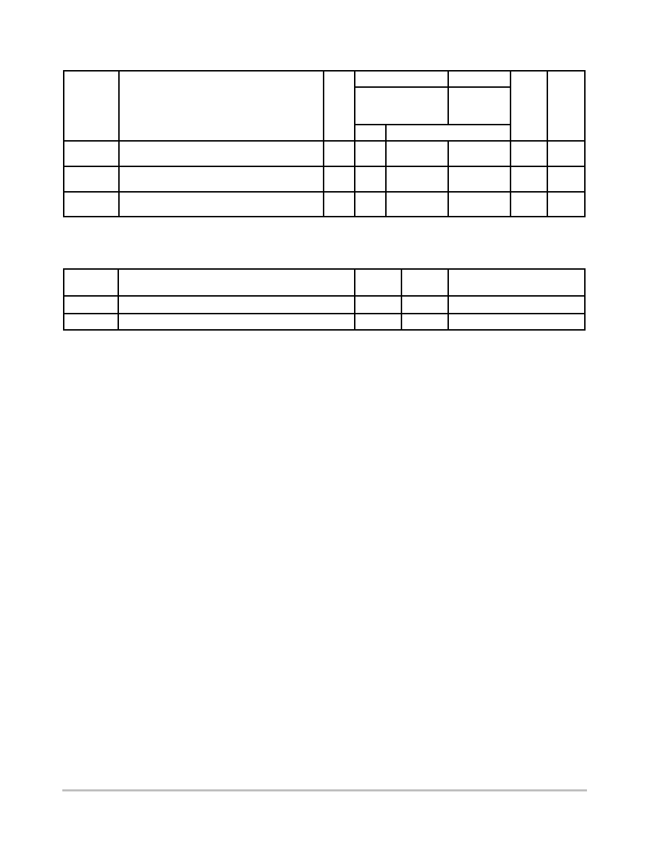
DC CHARACTERISTICS
74ACT
74ACT
Symbol
Parameter
VCC
(V)
TA = +25
°
C
TA =
40
°
C to
+85
°
C
Unit
Conditions
Typ
Guaranteed Limits
VIH
Minimum High Level
4.5
1.5
2.0
2.0
V
VOUT = 0.1 V
u
g
e e
Input Voltage
5.5
1.5
2.0
2.0
V
or VCC 0.1 V
VIL
Maximum Low Level
4.5
1.5
0.8
0.8
V
VOUT = 0.1 V
a
u
o
e e
Input Voltage
5.5
1.5
0.8
0.8
V
or VCC 0.1 V
VOH
Minimum High Level
4.5
4.49
4.4
4.4
V
IOUT = 50
µ
A
u
g
e e
Output Voltage
5.5
5.49
5.4
5.4
V
*VIN = VIL or VIH
4.5
3.86
3.76
V
IOH
24 mA
5.5
4.86
4.76
IOH
24 mA
VOL
Maximum Low Level
4.5
0.001
0.1
0.1
V
IOUT = 50
µ
A
a
u
o
e e
Output Voltage
5.5
0.001
0.1
0.1
V
*VIN = VIL or VIH
4.5
0.36
0.44
V
IOL
24 mA
5.5
0.36
0.44
IOL
24 mA
IIN
Maximum Input
5 5
±
0 1
±
1 0
µ
A
VI = VCC GND
a
u
u
Leakage Current
5.5
±
0.1
±
1.0
µ
A
VI = VCC, GND
ICCT
Additional Max. ICC/Input
5.5
0.6
1.5
mA
VI = VCC 2.1 V
IOZ
Maximum
VI (OE) = VIL, VIH
a
u
3-State
C
5.5
±
0.5
±
5.0
µ
A
VI = VCC, GND
Current
VO = VCC, GND
IOLD
Minimum Dynamic
O t
t C
t
5.5
75
mA
VOLD = 1.65 V Max
IOHD
Output Current
5.5
75
mA
VOHD = 3.85 V Min
ICC
Maximum Quiescent
5 5
8 0
80
µ
A
VIN = VCC or GND
a
u
Qu esce
Supply Current
5.5
8.0
80
µ
A
VIN = VCC or GND
*All outputs loaded; thresholds on input associated with output under test.
Maximum test duration 2.0 ms, one output loaded at a time.
AC CHARACTERISTICS (For Figures and Waveforms -- See Section 3)
74ACT
74ACT
Symbol
Parameter
VCC*
(V)
TA = +25
°
C
CL = 50 pF
TA = 40
°
C
to +85
°
C
CL = 50 pF
Unit
Fig.
No.
Min
Typ
Max
Min
Max
fma
Maximum Clock
5 0
100
85
ns
33
fmax
Maximum Clock
Frequency
5.0
100
85
ns
33
tPLH
Propagation Delay
5 0
2 5
11
2 0
12
ns
36
tPLH
Pro agation Delay
CP to On
5.0
2.5
11
2.0
12
ns
36
tPHL
Propagation Delay
5 0
2 0
10
1 5
11
ns
36
tPHL
Pro agation Delay
CP to On
5.0
2.0
10
1.5
11
ns
36
tPZH
Output Enable Time
5.0
2.0
9.5
1.5
10
ns
37
tPZL
Output Enable Time
5.0
2.0
9.0
1.5
10
ns
38
tPHZ
Output Disable Time
5.0
2.0
10.5
1.5
11.5
ns
37
tPLZ
Output Disable Time
5.0
2.0
8.5
1.5
9.0
ns
38
*Voltage Range 5.0 V is 5.0 V
±
0.5 V.
MC74AC574, MC74ACT574
http://onsemi.com
7
AC OPERATING REQUIREMENTS
74ACT
74ACT
Symbol
Parameter
VCC*
(V)
TA = +25
°
C
CL = 50 pF
TA = 40
°
C
to +85
°
C
CL = 50 pF
Unit
Fig.
No.
Typ
Guaranteed Minimum
ts
Setup Time, HIGH or LOW
5 0
2 5
2 5
ns
39
ts
Setu Time, HIGH or LOW
Dn to CP
5.0
2.5
2.5
ns
39
th
Hold Time, HIGH or LOW
5 0
1 0
1 0
ns
39
th
Hold Time, HIGH or LOW
Dn to CP
5.0
1.0
1.0
ns
39
tw
CP Pulse Width
5 0
3 0
4 0
ns
36
tw
CP Pulse Width
HIGH or LOW
5.0
3.0
4.0
ns
36
*Voltage Range 3.3 V is 3.3 V
±
0.3 V.
Voltage Range 5.0 V is 5.0 V
±
0.5 V.
CAPACITANCE
Symbol
Parameter
Value
Typ
Unit
Test Conditions
CIN
Input Capacitance
4.5
pF
VCC = 5.0 V
CPD
Power Dissipation Capacitance
40
pF
VCC = 5.0 V
MC74AC574, MC74ACT574
http://onsemi.com
8
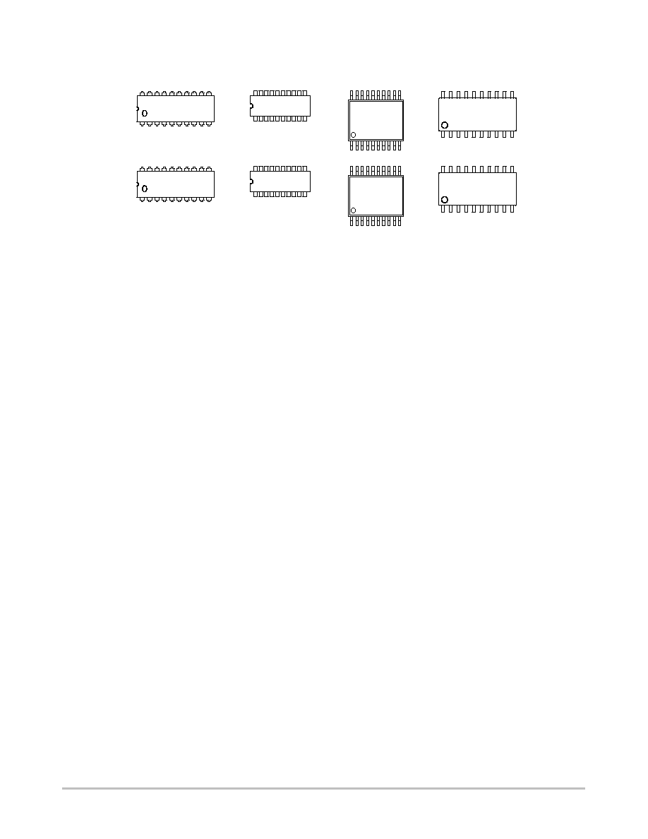
AC
574
ALYW
AC574
AWLYYWW
MC74AC574N
AWLYYWW
74AC574
AWLYWW
MARKING DIAGRAMS
PDIP20
SO20
TSSOP20
EIAJ20
ACT
574
ALYW
ACT574
AWLYYWW
MC74ACT574N
AWLYYWW
74ACT574
AWLYWW
A
= Assembly Location
WL, L
= Wafer Lot
YY, Y
= Year
WW, W = Work Week
MC74AC574, MC74ACT574
http://onsemi.com
9
PACKAGE DIMENSIONS
PDIP20
N SUFFIX
20 PIN PLASTIC DIP PACKAGE
CASE 73803
ISSUE E
NOTES:
1. DIMENSIONING AND TOLERANCING PER ANSI
Y14.5M, 1982.
2. CONTROLLING DIMENSION: INCH.
3. DIMENSION L TO CENTER OF LEAD WHEN
FORMED PARALLEL.
4. DIMENSION B DOES NOT INCLUDE MOLD
FLASH.
M
L
J
20 PL
M
B
M
0.25 (0.010)
T
DIM
MIN
MAX
MIN
MAX
MILLIMETERS
INCHES
A
25.66
27.17
1.010
1.070
B
6.10
6.60
0.240
0.260
C
3.81
4.57
0.150
0.180
D
0.39
0.55
0.015
0.022
G
2.54 BSC
0.100 BSC
J
0.21
0.38
0.008
0.015
K
2.80
3.55
0.110
0.140
L
7.62 BSC
0.300 BSC
M
0
15
0
15
N
0.51
1.01
0.020
0.040
_
_
_
_
E
1.27
1.77
0.050
0.070
1
11
10
20
A
SEATING
PLANE
K
N
F
G
D
20 PL
T
M
A
M
0.25 (0.010)
T
E
B
C
F
1.27 BSC
0.050 BSC
SO20
DW SUFFIX
20 PIN PLASTIC SOIC PACKAGE
CASE 751D05
ISSUE F
20
1
11
10
B
20X
H
10X
C
L
18X
A1
A
SEATING
PLANE
q
h
X 45
_
E
D
M
0.25
M
B
M
0.25
S
A
S
B
T
e
T
B
A
DIM
MIN
MAX
MILLIMETERS
A
2.35
2.65
A1
0.10
0.25
B
0.35
0.49
C
0.23
0.32
D
12.65
12.95
E
7.40
7.60
e
1.27 BSC
H
10.05
10.55
h
0.25
0.75
L
0.50
0.90
q
0
7
NOTES:
1. DIMENSIONS ARE IN MILLIMETERS.
2. INTERPRET DIMENSIONS AND TOLERANCES
PER ASME Y14.5M, 1994.
3. DIMENSIONS D AND E DO NOT INCLUDE MOLD
PROTRUSION.
4. MAXIMUM MOLD PROTRUSION 0.15 PER SIDE.
5. DIMENSION B DOES NOT INCLUDE DAMBAR
PROTRUSION. ALLOWABLE PROTRUSION SHALL
BE 0.13 TOTAL IN EXCESS OF B DIMENSION AT
MAXIMUM MATERIAL CONDITION.
_
_
MC74AC574, MC74ACT574
http://onsemi.com
10
PACKAGE DIMENSIONS
TSSOP20
DT SUFFIX
20 PIN PLASTIC TSSOP PACKAGE
CASE 948E02
ISSUE A
DIM
A
MIN
MAX
MIN
MAX
INCHES
6.60
0.260
MILLIMETERS
B
4.30
4.50
0.169
0.177
C
1.20
0.047
D
0.05
0.15
0.002
0.006
F
0.50
0.75
0.020
0.030
G
0.65 BSC
0.026 BSC
H
0.27
0.37
0.011
0.015
J
0.09
0.20
0.004
0.008
J1
0.09
0.16
0.004
0.006
K
0.19
0.30
0.007
0.012
K1
0.19
0.25
0.007
0.010
L
6.40 BSC
0.252 BSC
M
0 8 0 8
_
_
_
_
NOTES:
1. DIMENSIONING AND TOLERANCING PER ANSI
Y14.5M, 1982.
2. CONTROLLING DIMENSION: MILLIMETER.
3. DIMENSION A DOES NOT INCLUDE MOLD
FLASH, PROTRUSIONS OR GATE BURRS. MOLD
FLASH OR GATE BURRS SHALL NOT EXCEED
0.15 (0.006) PER SIDE.
4. DIMENSION B DOES NOT INCLUDE
INTERLEAD FLASH OR PROTRUSION.
INTERLEAD FLASH OR PROTRUSION SHALL NOT
EXCEED 0.25 (0.010) PER SIDE.
5. DIMENSION K DOES NOT INCLUDE DAMBAR
PROTRUSION. ALLOWABLE DAMBAR
PROTRUSION SHALL BE 0.08 (0.003) TOTAL IN
EXCESS OF THE K DIMENSION AT MAXIMUM
MATERIAL CONDITION.
6. TERMINAL NUMBERS ARE SHOWN FOR
REFERENCE ONLY.
7. DIMENSION A AND B ARE TO BE
DETERMINED AT DATUM PLANE -W-.
ÍÍÍ
ÍÍÍ
ÍÍÍ
1
10
11
20
PIN 1
IDENT
A
B
T
0.100 (0.004)
C
D
G
H
SECTION NN
K
K1
J J1
N
N
M
F
W
SEATING
PLANE
V
U
S
U
M
0.10 (0.004)
V
S
T
20X REF
K
L
L/2
2X
S
U
0.15 (0.006) T
DETAIL E
0.25 (0.010)
DETAIL E
6.40
0.252
---
---
S
U
0.15 (0.006) T
EIAJ20
M SUFFIX
20 PIN PLASTIC EIAJ PACKAGE
CASE 96701
ISSUE O
DIM
MIN
MAX
MIN
MAX
INCHES
---
2.05
---
0.081
MILLIMETERS
0.05
0.20
0.002
0.008
0.35
0.50
0.014
0.020
0.18
0.27
0.007
0.011
12.35
12.80
0.486
0.504
5.10
5.45
0.201
0.215
1.27 BSC
0.050 BSC
7.40
8.20
0.291
0.323
0.50
0.85
0.020
0.033
1.10
1.50
0.043
0.059
0
0.70
0.90
0.028
0.035
---
0.81
---
0.032
A1
HE
Q1
LE
_
10
_
0
_
10
_
NOTES:
1. DIMENSIONING AND TOLERANCING PER ANSI
Y14.5M, 1982.
2. CONTROLLING DIMENSION: MILLIMETER.
3. DIMENSIONS D AND E DO NOT INCLUDE
MOLD FLASH OR PROTRUSIONS AND ARE
MEASURED AT THE PARTING LINE. MOLD FLASH
OR PROTRUSIONS SHALL NOT EXCEED 0.15
(0.006) PER SIDE.
4. TERMINAL NUMBERS ARE SHOWN FOR
REFERENCE ONLY.
5. THE LEAD WIDTH DIMENSION (b) DOES NOT
INCLUDE DAMBAR PROTRUSION. ALLOWABLE
DAMBAR PROTRUSION SHALL BE 0.08 (0.003)
TOTAL IN EXCESS OF THE LEAD WIDTH
DIMENSION AT MAXIMUM MATERIAL CONDITION.
DAMBAR CANNOT BE LOCATED ON THE LOWER
RADIUS OR THE FOOT. MINIMUM SPACE
BETWEEN PROTRUSIONS AND ADJACENT LEAD
TO BE 0.46 ( 0.018).
HE
A1
LE
Q1
_
c
A
Z
D
E
20
1
10
11
b
M
0.13 (0.005)
e
0.10 (0.004)
VIEW P
DETAIL P
M
L
A
b
c
D
E
e
L
M
Z

MC74AC574, MC74ACT574
http://onsemi.com
11
Notes
MC74AC574, MC74ACT574
http://onsemi.com
12
ON Semiconductor and are trademarks of Semiconductor Components Industries, LLC (SCILLC). SCILLC reserves the right to make changes
without further notice to any products herein. SCILLC makes no warranty, representation or guarantee regarding the suitability of its products for any particular
purpose, nor does SCILLC assume any liability arising out of the application or use of any product or circuit, and specifically disclaims any and all liability,
including without limitation special, consequential or incidental damages. "Typical" parameters which may be provided in SCILLC data sheets and/or
specifications can and do vary in different applications and actual performance may vary over time. All operating parameters, including "Typicals" must be
validated for each customer application by customer's technical experts. SCILLC does not convey any license under its patent rights nor the rights of others.
SCILLC products are not designed, intended, or authorized for use as components in systems intended for surgical implant into the body, or other applications
intended to support or sustain life, or for any other application in which the failure of the SCILLC product could create a situation where personal injury or
death may occur. Should Buyer purchase or use SCILLC products for any such unintended or unauthorized application, Buyer shall indemnify and hold
SCILLC and its officers, employees, subsidiaries, affiliates, and distributors harmless against all claims, costs, damages, and expenses, and reasonable
attorney fees arising out of, directly or indirectly, any claim of personal injury or death associated with such unintended or unauthorized use, even if such claim
alleges that SCILLC was negligent regarding the design or manufacture of the part. SCILLC is an Equal Opportunity/Affirmative Action Employer.
PUBLICATION ORDERING INFORMATION
JAPAN: ON Semiconductor, Japan Customer Focus Center
4321 NishiGotanda, Shinagawaku, Tokyo, Japan 1410031
Phone: 81357402700
Email: r14525@onsemi.com
ON Semiconductor Website: http://onsemi.com
For additional information, please contact your local
Sales Representative.
MC74AC574/D
Literature Fulfillment:
Literature Distribution Center for ON Semiconductor
P.O. Box 5163, Denver, Colorado 80217 USA
Phone: 3036752175 or 8003443860 Toll Free USA/Canada
Fax: 3036752176 or 8003443867 Toll Free USA/Canada
Email: ONlit@hibbertco.com
N. American Technical Support: 8002829855 Toll Free USA/Canada