
Quad 2 Input NOR Gate
∑
Outputs Source/Sink 24 mA
∑
ACT02 Has TTL Compatible Inputs
13
14
12
11
10
9
8
2
1
3
4
5
6
7
GND
V
CC
Figure 1. Pinout: 14≠Lead Packages Conductors
(Top View)
MAXIMUM RATINGS*
Symbol
Parameter
Value
Unit
V
CC
DC Supply Voltage (Referenced to GND)
≠0.5 to +7.0
V
V
in
DC Input Voltage (Referenced to GND)
≠0.5 to V
CC
+0.5
V
V
out
DC Output Voltage (Referenced to GND)
≠0.5 to V
CC
+0.5
V
I
in
DC Input Current, per Pin
±
20
mA
I
out
DC Output Sink/Source Current, per Pin
±
50
mA
I
CC
DC V
CC
or GND Current per Output Pin
±
50
mA
T
stg
Storage Temperature
≠65 to +150
∞
C
* Maximum Ratings are those values beyond which damage to the device may occur. Functional
operation should be restricted to the Recommended Operating Conditions.
RECOMMENDED OPERATING CONDITIONS
Symbol
Parameter
Min
Typ
Max
Unit
V
Supply Voltage
AC
2.0
5.0
6.0
V
V
CC
Supply Voltage
ACT
4.5
5.0
5.5
V
V
in
, V
out
DC Input Voltage, Output Voltage (Ref. to GND)
0
V
CC
V
V
CC
@ 3.0 V
150
t
r
, t
f
Input Rise and Fall Time (Note 1)
AC Devices except Schmitt Inputs
V
CC
@ 4.5 V
40
ns/V
r
,
f
AC Devices except Schmitt Inputs
V
CC
@ 5.5 V
25
t t
Input Rise and Fall Time (Note 2)
V
CC
@ 4.5 V
10
ns/V
t
r
, t
f
In ut Rise and Fall Time (Note 2)
ACT Devices except Schmitt Inputs
V
CC
@ 5.5 V
8.0
ns/V
T
J
Junction Temperature (PDIP)
140
∞
C
T
A
Operating Ambient Temperature Range
≠40
25
85
∞
C
I
OH
Output Current -- High
≠24
mA
I
OL
Output Current -- Low
24
mA
1. V
in
from 30% to 70% V
CC
; see individual Data Sheets for devices that differ from the typical input rise and fall times.
2. V
in
from 0.8 V to 2.0 V; see individual Data Sheets for devices that differ from the typical input rise and fall times.
©
Semiconductor Components Industries, LLC, 2001
January, 2001 ≠ Rev. 4
1
Publication Order Number:
MC74AC02/D
MC74AC02
MC74ACT02
QUAD 2-INPUT
NOR GATE
N SUFFIX
CASE 646-06
PLASTIC
D SUFFIX
CASE 751A-03
PLASTIC

MC74AC02 MC74ACT02
http://onsemi.com
2
DC CHARACTERISTICS
74AC
74AC
Symbol
Parameter
V
CC
(V)
T
A
= +25
∞
C
T
A
=
≠40
∞
C to
+85
∞
C
Unit
Conditions
Typ
Guaranteed Limits
V
IH
Minimum High Level
3.0
1.5
2.1
2.1
V
OUT
= 0.1 V
g
Input Voltage
4.5
2.25
3.15
3.15
V
or V
CC
≠ 0.1 V
5.5
2.75
3.85
3.85
V
IL
Maximum Low Level
3.0
1.5
0.9
0.9
V
OUT
= 0.1 V
Input Voltage
4.5
2.25
1.35
1.35
V
or V
CC
≠ 0.1 V
5.5
2.75
1.65
1.65
V
OH
Minimum High Level
3.0
2.99
2.9
2.9
I
OUT
= ≠50
µ
A
g
Output Voltage
4.5
4.49
4.4
4.4
V
5.5
5.49
5.4
5.4
*V
IN
= V
IL
or V
IH
3.0
2.56
2.46
V
≠12 mA
4.5
3.86
3.76
V
I
OH
≠24 mA
5.5
4.86
4.76
≠24 mA
V
OL
Maximum Low Level
3.0
0.002
0.1
0.1
I
OUT
= 50
µ
A
Output Voltage
4.5
0.001
0.1
0.1
V
5.5
0.001
0.1
0.1
*V
IN
= V
IL
or V
IH
3.0
0.36
0.44
V
12 mA
4.5
0.36
0.44
V
I
OL
24 mA
5.5
0.36
0.44
24 mA
I
IN
Maximum Input
5 5
±
0 1
±
1 0
µ
A
V
I
= V
CC
GND
Leakage Current
5.5
±
0.1
±
1.0
µ
A
V
I
= V
CC
, GND
I
OLD
Minimum Dynamic
O t
t C
t
5.5
75
mA
V
OLD
= 1.65 V Max
I
OHD
Output Current
5.5
≠75
mA
V
OHD
= 3.85 V Min
I
CC
Maximum Quiescent
5 5
4 0
40
µ
A
V
IN
= V
CC
or GND
Q
Supply Current
5.5
4.0
40
µ
A
V
IN
= V
CC
or GND
* All outputs loaded; thresholds on input associated with output under test.
Maximum test duration 2.0 ms, one output loaded at a time.
Note: I
IN
and I
CC
@ 3.0 V are guaranteed to be less than or equal to the respective limit @ 5.5 V V
CC
.
AC CHARACTERISTICS
(For Figures and Waveforms -- See Section 3 of the ON Semiconductor FACT Data Book, DL138/D)
74AC
74AC
Symbol
Parameter
V
CC
*
(V)
T
A
= +25
∞
C
C
L
= 50 pF
T
A
= ≠40
∞
C
to +85
∞
C
C
L
= 50 pF
Unit
Fig.
No.
Min
Typ
Max
Min
Max
t
PLH
Propagation Delay
3.3
1.5
5.0
7.5
1.0
8.0
ns
3-5
t
PLH
Propagation Delay
5.0
1.5
4.0
6.0
1.0
6.5
ns
3-5
t
PHL
Propagation Delay
3.3
1.5
5.0
7.5
1.0
8.0
ns
3-5
t
PHL
Propagation Delay
5.0
1.5
4.5
6.5
1.0
7.0
ns
3-5
* Voltage Range 3.3 V is 3.3 V
±
0.3 V.
Voltage Range 5.0 V is 5.0 V
±
0.5 V.

MC74AC02 MC74ACT02
http://onsemi.com
3
DC CHARACTERISTICS
74ACT
74ACT
Symbol
Parameter
V
CC
(V)
T
A
= +25
∞
C
T
A
=
≠40
∞
C to
+85
∞
C
Unit
Conditions
Typ
Guaranteed Limits
V
IH
Minimum High Level
4.5
1.5
2.0
2.0
V
V
OUT
= 0.1 V
g
Input Voltage
5.5
1.5
2.0
2.0
V
or V
CC
≠ 0.1 V
V
IL
Maximum Low Level
4.5
1.5
0.8
0.8
V
V
OUT
= 0.1 V
Input Voltage
5.5
1.5
0.8
0.8
V
or V
CC
≠ 0.1 V
V
OH
Minimum High Level
4.5
4.49
4.4
4.4
V
I
OUT
= ≠50
µ
A
g
Output Voltage
5.5
5.49
5.4
5.4
V
*V
IN
= V
IL
or V
IH
4.5
3.86
3.76
V
I
OH
≠24 mA
5.5
4.86
4.76
I
OH
≠24 mA
V
OL
Maximum Low Level
4.5
0.001
0.1
0.1
V
I
OUT
= 50
µ
A
Output Voltage
5.5
0.001
0.1
0.1
V
*V
IN
= V
IL
or V
IH
4.5
0.36
0.44
V
I
OL
24 mA
5.5
0.36
0.44
I
OL
24 mA
I
IN
Maximum Input
5 5
±
0 1
±
1 0
µ
A
V
I
= V
CC
GND
Leakage Current
5.5
±
0.1
±
1.0
µ
A
V
I
= V
CC
, GND
I
CCT
Additional Max. I
CC
/Input
5.5
0.6
1.5
mA
V
I
= V
CC
≠ 2.1 V
I
OLD
Minimum Dynamic
O t
t C
t
5.5
75
mA
V
OLD
= 1.65 V Max
I
OHD
Output Current
5.5
≠75
mA
V
OHD
= 3.85 V Min
I
CC
Maximum Quiescent
5 5
4 0
40
µ
A
V
IN
= V
CC
or GND
Q
Supply Current
5.5
4.0
40
µ
A
V
IN
= V
CC
or GND
* All outputs loaded; thresholds on input associated with output under test.
Maximum test duration 2.0 ms, one output loaded at a time.
AC CHARACTERISTICS
(For Figures and Waveforms -- See Section 3 of the ON Semiconductor FACT Data Book, DL138/D)
74ACT
74ACT
Symbol
Parameter
V
CC
*
(V)
T
A
= +25
∞
C
C
L
= 50 pF
T
A
= ≠40
∞
C
to +85
∞
C
C
L
= 50 pF
Unit
Fig.
No.
Min
Typ
Max
Min
Max
t
PLH
Propagation Delay
5.0
1.5
8.5
1.0
9.0
ns
3-6
t
PHL
Propagation Delay
5.0
1.5
9.5
1.0
10
ns
3-6
* Voltage Range 5.0 V is 5.0 V
±
0.5 V.
CAPACITANCE
Symbol
Parameter
Value
Typ
Unit
Test Conditions
C
IN
Input Capacitance
4.5
pF
V
CC
= 5.0 V
C
PD
Power Dissipation Capacitance
30
pF
V
CC
= 5.0 V
MC74AC02 MC74ACT02
http://onsemi.com
4
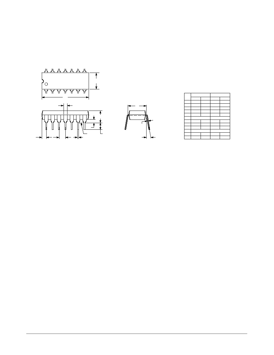
OUTLINE DIMENSIONS
N SUFFIX
PLASTIC DIP PACKAGE
CASE 646≠06
ISSUE L
NOTES:
1. LEADS WITHIN 0.13 (0.005) RADIUS OF TRUE
POSITION AT SEATING PLANE AT MAXIMUM
MATERIAL CONDITION.
2. DIMENSION L TO CENTER OF LEADS WHEN
FORMED PARALLEL.
3. DIMENSION B DOES NOT INCLUDE MOLD
FLASH.
4. ROUNDED CORNERS OPTIONAL.
1
7
14
8
B
A
F
H
G
D
K
C
N
L
J
M
SEATING
PLANE
DIM
MIN
MAX
MIN
MAX
MILLIMETERS
INCHES
A
0.715
0.770
18.16
19.56
B
0.240
0.260
6.10
6.60
C
0.145
0.185
3.69
4.69
D
0.015
0.021
0.38
0.53
F
0.040
0.070
1.02
1.78
G
0.100 BSC
2.54 BSC
H
0.052
0.095
1.32
2.41
J
0.008
0.015
0.20
0.38
K
0.115
0.135
2.92
3.43
L
0.300 BSC
7.62 BSC
M
0
10
0
10
N
0.015
0.039
0.39
1.01
_
_
_
_

MC74AC02 MC74ACT02
http://onsemi.com
5
OUTLINE DIMENSIONS
D SUFFIX
PLASTIC SOIC PACKAGE
CASE 751A≠03
ISSUE F
NOTES:
1. DIMENSIONING AND TOLERANCING PER
ANSI Y14.5M, 1982.
2. CONTROLLING DIMENSION: MILLIMETER.
3. DIMENSIONS A AND B DO NOT INCLUDE
MOLD PROTRUSION.
4. MAXIMUM MOLD PROTRUSION 0.15 (0.006)
PER SIDE.
5. DIMENSION D DOES NOT INCLUDE DAMBAR
PROTRUSION. ALLOWABLE DAMBAR
PROTRUSION SHALL BE 0.127 (0.005) TOTAL
IN EXCESS OF THE D DIMENSION AT
MAXIMUM MATERIAL CONDITION.
≠A≠
≠B≠
G
P
7 PL
14
8
7
1
M
0.25 (0.010)
B
M
S
B
M
0.25 (0.010)
A
S
T
≠T≠
F
R
X 45
SEATING
PLANE
D
14 PL
K
C
J
M
_
DIM
MIN
MAX
MIN
MAX
INCHES
MILLIMETERS
A
8.55
8.75
0.337
0.344
B
3.80
4.00
0.150
0.157
C
1.35
1.75
0.054
0.068
D
0.35
0.49
0.014
0.019
F
0.40
1.25
0.016
0.049
G
1.27 BSC
0.050 BSC
J
0.19
0.25
0.008
0.009
K
0.10
0.25
0.004
0.009
M
0
7
0
7
P
5.80
6.20
0.228
0.244
R
0.25
0.50
0.010
0.019
_
_
_
_