ƒÓÍÛÏÂÌÚýˆËˇ Ë ÓÔËÒýÌˡ www.docs.chipfind.ru
©
Semiconductor Components Industries, LLC, 2000
May, 2000 ≠ Rev. 9
1
Publication Order Number:
MC74HC573A/D
MC74HC573A
Octal 3-State Noninverting
Transparent Latch
High≠Performance Silicon≠Gate CMOS
The MC74HC573A is identical in pinout to the LS573. The devices
are compatible with standard CMOS outputs; with pullup resistors,
they are compatible with LSTTL outputs.
These latches appear transparent to data (i.e., the outputs change
asynchronously) when Latch Enable is high. When Latch Enable goes
low, data meeting the setup and hold time becomes latched.
The HC573A is identical in function to the HC373A but has the data
inputs on the opposite side of the package from the outputs to facilitate
PC board layout.
∑
Output Drive Capability: 15 LSTTL Loads
∑
Outputs Directly Interface to CMOS, NMOS and TTL
∑
Operating Voltage Range: 2.0 to 6.0 V
∑
Low Input Current: 1.0
µ
A
∑
In Compliance with the Requirements Defined by JEDEC Standard
No. 7A
∑
Chip Complexity: 218 FETs or 54.5 Equivalent Gates
http://onsemi.com
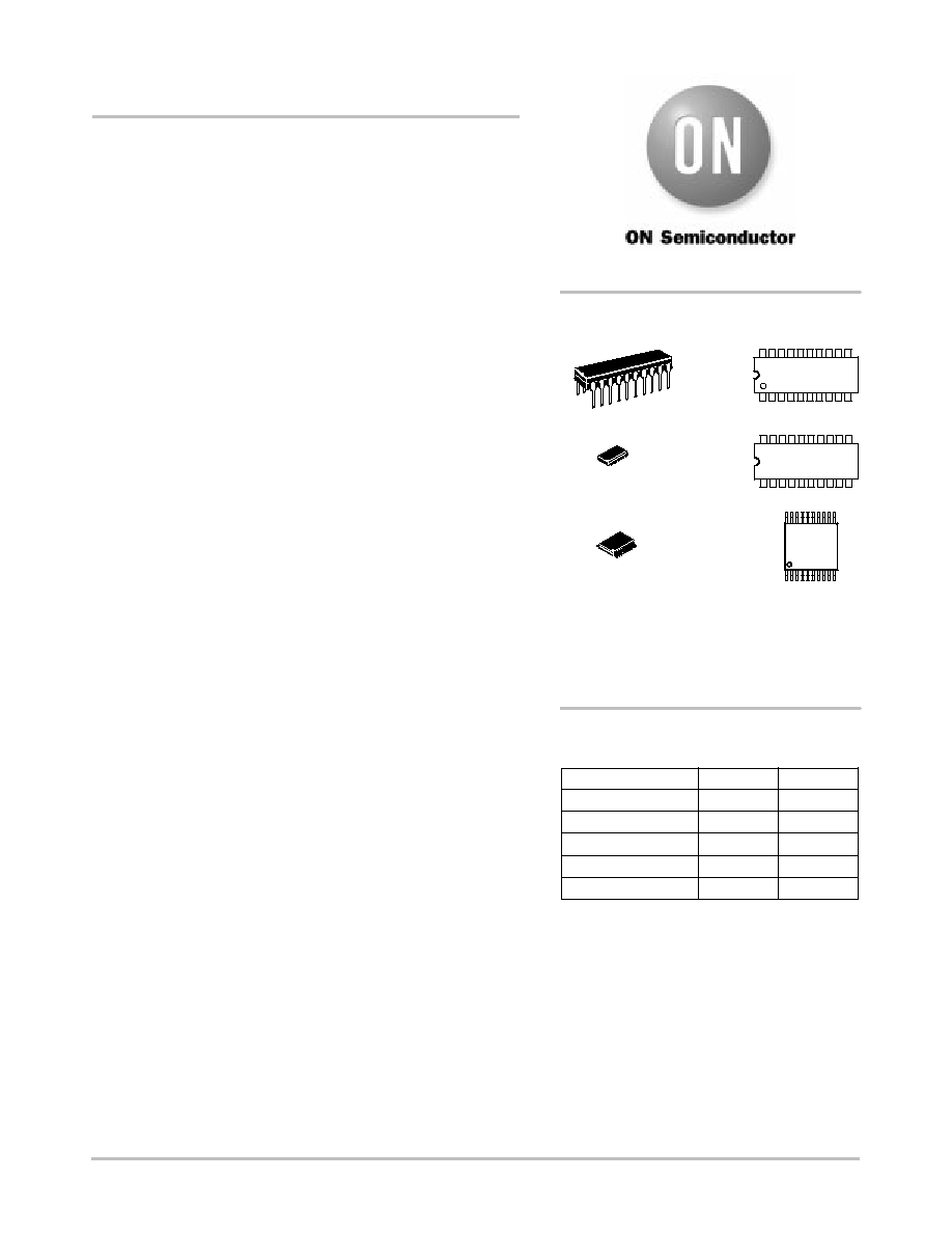
MARKING
DIAGRAMS
1
20
A
= Assembly Location
WL = Wafer Lot
YY = Year
WW = Work Week
SOIC WIDE≠20
DW SUFFIX
CASE 751D
HC573A
AWLYYWW
PDIP≠20
N SUFFIX
CASE 738
1
20
MC74HC573AN
AWLYYWW
TSSOP≠20
DT SUFFIX
CASE 948E
1
20
1
20
1
20
Device
Package
Shipping
ORDERING INFORMATION
MC74HC573AN
PDIP≠20
1440 / Box
MC74HC573ADW
SOIC≠WIDE
38 / Rail
MC74HC573ADWR2
SOIC≠WIDE
1000 / Reel
MC74HC573ADT
TSSOP≠20
75 / Rail
MC74HC573ADTR2
TSSOP≠20
2500 / Reel
HC
573A
ALYW
1
20
MC74HC573A
http://onsemi.com
2
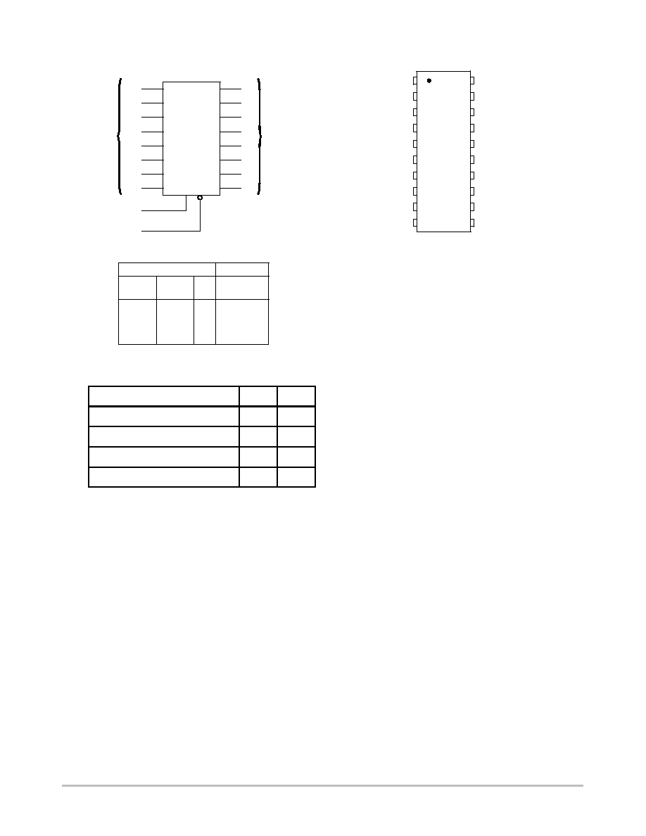
LOGIC DIAGRAM
DATA
INPUTS
D0
D1
D2
D3
D4
D5
D6
D7
LATCH ENABLE
OUTPUT ENABLE
11
1
9
8
7
6
5
4
3
2
19
18
17
16
15
14
13
12
Q0
Q1
Q2
Q3
Q4
Q5
Q6
Q7
PIN 20 = VCC
PIN 10 = GND
NONINVERTING
OUTPUTS
PIN ASSIGNMENT
D4
D2
D1
D0
OUTPUT
ENABLE
GND
D7
D6
D5
D3
5
4
3
2
1
10
9
8
7
6
14
15
16
17
18
19
20
11
12
13
Q3
Q2
Q1
Q0
VCC
LATCH
ENABLE
Q7
Q6
Q5
Q4
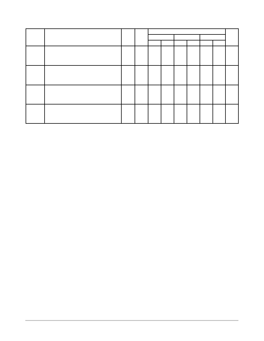
FUNCTION TABLE
Inputs
Output
Output
Latch
Enable
Enable
D
Q
L
H
H
H
L
H
L
L
L
L
X
No Change
H
X
X
Z
X = Don't Care
Z = High Impedance
ŒŒŒŒŒŒŒŒŒŒ
Œ
ŒŒŒŒŒŒŒŒ
Œ
ŒŒŒŒŒŒŒŒŒŒ
Design Criteria
ŒŒŒŒ
Œ
ŒŒ
Œ
ŒŒŒŒ
Value
ŒŒŒ
Œ
Œ
Œ
ŒŒŒ
Units
ŒŒŒŒŒŒŒŒŒŒ
ŒŒŒŒŒŒŒŒŒŒ
Internal Gate Count*
ŒŒŒŒ
ŒŒŒŒ
54.5
ŒŒŒ
ŒŒŒ
ea.
ŒŒŒŒŒŒŒŒŒŒ
ŒŒŒŒŒŒŒŒŒŒ
Internal Gate Propagation Delay
ŒŒŒŒ
ŒŒŒŒ
1.5
ŒŒŒ
ŒŒŒ
ns
ŒŒŒŒŒŒŒŒŒŒ
ŒŒŒŒŒŒŒŒŒŒ
Internal Gate Power Dissipation
ŒŒŒŒ
ŒŒŒŒ
5.0
ŒŒŒ
ŒŒŒ
µ
W
ŒŒŒŒŒŒŒŒŒŒ
Œ
ŒŒŒŒŒŒŒŒ
Œ
ŒŒŒŒŒŒŒŒŒŒ
Speed Power Product
ŒŒŒŒ
Œ
ŒŒ
Œ
ŒŒŒŒ
0.0075
ŒŒŒ
Œ
Œ
Œ
ŒŒŒ
pJ
*Equivalent to a two≠input NAND gate.
MC74HC573A
http://onsemi.com
3
ŒŒŒŒŒŒŒŒŒŒŒŒŒŒŒŒŒŒŒŒŒŒŒ
ŒŒŒŒŒŒŒŒŒŒŒŒŒŒŒŒŒŒŒŒŒŒŒ
MAXIMUM RATINGS*
ŒŒŒŒ
ŒŒŒŒ
Symbol
ŒŒŒŒŒŒŒŒŒŒŒŒŒŒ
ŒŒŒŒŒŒŒŒŒŒŒŒŒŒ
Parameter
ŒŒŒŒŒ
ŒŒŒŒŒ
Value
ŒŒŒ
ŒŒŒ
Unit
ŒŒŒŒ
ŒŒŒŒ
VCC
ŒŒŒŒŒŒŒŒŒŒŒŒŒŒ
ŒŒŒŒŒŒŒŒŒŒŒŒŒŒ
DC Supply Voltage (Referenced to GND)
ŒŒŒŒŒ
ŒŒŒŒŒ
≠ 0.5 to + 7.0
ŒŒŒ
ŒŒŒ
V
ŒŒŒŒ
ŒŒŒŒ
Vin
ŒŒŒŒŒŒŒŒŒŒŒŒŒŒ
ŒŒŒŒŒŒŒŒŒŒŒŒŒŒ
DC Input Voltage (Referenced to GND)
ŒŒŒŒŒ
ŒŒŒŒŒ
≠ 0.5 to VCC + 0.5
ŒŒŒ
ŒŒŒ
V
ŒŒŒŒ
ŒŒŒŒ
Vout
ŒŒŒŒŒŒŒŒŒŒŒŒŒŒ
ŒŒŒŒŒŒŒŒŒŒŒŒŒŒ
DC Output Voltage (Referenced to GND)
ŒŒŒŒŒ
ŒŒŒŒŒ
≠ 0.5 to VCC + 0.5
ŒŒŒ
ŒŒŒ
V
ŒŒŒŒ
ŒŒŒŒ
Iin
ŒŒŒŒŒŒŒŒŒŒŒŒŒŒ
ŒŒŒŒŒŒŒŒŒŒŒŒŒŒ
DC Input Current, per Pin
ŒŒŒŒŒ
ŒŒŒŒŒ
±
20
ŒŒŒ
ŒŒŒ
mA
ŒŒŒŒ
ŒŒŒŒ
Iout
ŒŒŒŒŒŒŒŒŒŒŒŒŒŒ
ŒŒŒŒŒŒŒŒŒŒŒŒŒŒ
DC Output Current, per Pin
ŒŒŒŒŒ
ŒŒŒŒŒ
±
35
ŒŒŒ
ŒŒŒ
mA
ŒŒŒŒ
ŒŒŒŒ
ICC
ŒŒŒŒŒŒŒŒŒŒŒŒŒŒ
ŒŒŒŒŒŒŒŒŒŒŒŒŒŒ
DC Supply Current, VCC and GND Pins
ŒŒŒŒŒ
ŒŒŒŒŒ
±
75
ŒŒŒ
ŒŒŒ
mA
ŒŒŒŒ
Œ
ŒŒ
Œ
ŒŒŒŒ
PD
ŒŒŒŒŒŒŒŒŒŒŒŒŒŒ
Œ
ŒŒŒŒŒŒŒŒŒŒŒŒ
Œ
ŒŒŒŒŒŒŒŒŒŒŒŒŒŒ
Power Dissipation in Still Air,
Plastic DIP
SOIC Package
TSSOP Package
ŒŒŒŒŒ
Œ
ŒŒŒ
Œ
ŒŒŒŒŒ
750
500
450
ŒŒŒ
Œ
Œ
Œ
ŒŒŒ
mW
ŒŒŒŒ
ŒŒŒŒ
Tstg
ŒŒŒŒŒŒŒŒŒŒŒŒŒŒ
ŒŒŒŒŒŒŒŒŒŒŒŒŒŒ
Storage Temperature
ŒŒŒŒŒ
ŒŒŒŒŒ
≠ 65 to + 150
ŒŒŒ
ŒŒŒ
_
C
ŒŒŒŒ
Œ
ŒŒ
Œ
ŒŒŒŒ
TL
ŒŒŒŒŒŒŒŒŒŒŒŒŒŒ
Œ
ŒŒŒŒŒŒŒŒŒŒŒŒ
Œ
ŒŒŒŒŒŒŒŒŒŒŒŒŒŒ
Lead Temperature, 1 mm from Case for 10 Seconds
(Plastic DIP, TSSOP or SOIC Package)
ŒŒŒŒŒ
Œ
ŒŒŒ
Œ
ŒŒŒŒŒ
260
ŒŒŒ
Œ
Œ
Œ
ŒŒŒ
_
C
*Maximum Ratings are those values beyond which damage to the device may occur.
Functional operation should be restricted to the Recommended Operating Conditions.
Derating -- Plastic DIP: ≠ 10 mW/
_
C from 65
_
to 125
_
C
SOIC Package: ≠ 7 mW/
_
C from 65
_
to 125
_
C
TSSOP Package: ≠6.1 mW/
∞
C from 65
_
to 125
_
C
For high frequency or heavy load considerations, see Chapter 2 of the ON Semiconductor High≠Speed CMOS Data Book (DL129/D).
RECOMMENDED OPERATING CONDITIONS
ŒŒŒŒ
ŒŒŒŒ
Symbol
ŒŒŒŒŒŒŒŒŒŒŒŒŒŒŒ
ŒŒŒŒŒŒŒŒŒŒŒŒŒŒŒ
Parameter
ŒŒŒ
ŒŒŒ
Min
ŒŒ
ŒŒ
Max
ŒŒŒ
ŒŒŒ
Unit
ŒŒŒŒ
ŒŒŒŒ
VCC
ŒŒŒŒŒŒŒŒŒŒŒŒŒŒŒ
ŒŒŒŒŒŒŒŒŒŒŒŒŒŒŒ
DC Supply Voltage (Referenced to GND)
ŒŒŒ
ŒŒŒ
2.0
ŒŒ
ŒŒ
6.0
ŒŒŒ
ŒŒŒ
V
ŒŒŒŒ
ŒŒŒŒ
Vin, Vout
ŒŒŒŒŒŒŒŒŒŒŒŒŒŒŒ
ŒŒŒŒŒŒŒŒŒŒŒŒŒŒŒ
DC Input Voltage, Output Voltage (Referenced to GND)
ŒŒŒ
ŒŒŒ
0
ŒŒ
ŒŒ
VCC
ŒŒŒ
ŒŒŒ
V
ŒŒŒŒ
ŒŒŒŒ
TA
ŒŒŒŒŒŒŒŒŒŒŒŒŒŒŒ
ŒŒŒŒŒŒŒŒŒŒŒŒŒŒŒ
Operating Temperature, All Package Types
ŒŒŒ
ŒŒŒ
≠ 55
ŒŒ
ŒŒ
+ 125
ŒŒŒ
ŒŒŒ
_
C
ŒŒŒŒ
Œ
ŒŒ
Œ
ŒŒŒŒ
tr, tf
ŒŒŒŒŒŒŒŒŒŒŒŒŒŒŒ
Œ
ŒŒŒŒŒŒŒŒŒŒŒŒŒ
Œ
ŒŒŒŒŒŒŒŒŒŒŒŒŒŒŒ
Input Rise and Fall Time
VCC = 2.0 V
(Figure 1)
VCC = 4.5 V
VCC = 6.0 V
ŒŒŒ
Œ
Œ
Œ
ŒŒŒ
0
0
0
ŒŒ
ŒŒ
ŒŒ
1000
500
400
ŒŒŒ
Œ
Œ
Œ
ŒŒŒ
ns
DC ELECTRICAL CHARACTERISTICS
(Voltages Referenced to GND)
ŒŒŒŒ
ŒŒŒŒ
ŒŒŒŒŒŒŒŒŒ
ŒŒŒŒŒŒŒŒŒ
ŒŒŒŒŒŒŒŒŒ
ŒŒŒŒŒŒŒŒŒ
ŒŒŒŒ
ŒŒŒŒ
ŒŒŒŒŒŒŒŒŒ
ŒŒŒŒŒŒŒŒŒ
Guaranteed Limit
ŒŒŒ
ŒŒŒ
ŒŒŒŒ
ŒŒŒŒ
Symbol
ŒŒŒŒŒŒŒŒŒ
ŒŒŒŒŒŒŒŒŒ
Parameter
ŒŒŒŒŒŒŒŒŒ
ŒŒŒŒŒŒŒŒŒ
Test Conditions
ŒŒŒŒ
ŒŒŒŒ
VCC
V
ŒŒŒŒ
ŒŒŒŒ
≠ 55 to
25
_
C
ŒŒŒ
ŒŒŒ
v
85
_
C
ŒŒŒŒ
ŒŒŒŒ
v
125
_
C
ŒŒŒ
ŒŒŒ
Unit
ŒŒŒŒ
Œ
ŒŒ
Œ
Œ
ŒŒ
Œ
ŒŒŒŒ
VIH
ŒŒŒŒŒŒŒŒŒ
Œ
ŒŒŒŒŒŒŒ
Œ
Œ
ŒŒŒŒŒŒŒ
Œ
ŒŒŒŒŒŒŒŒŒ
Minimum High≠Level Input
Voltage
ŒŒŒŒŒŒŒŒŒ
Œ
ŒŒŒŒŒŒŒ
Œ
Œ
ŒŒŒŒŒŒŒ
Œ
ŒŒŒŒŒŒŒŒŒ
Vout = 0.1 V or VCC ≠ 0.1 V
|Iout|
v
20
µ
A
ŒŒŒŒ
Œ
ŒŒ
Œ
Œ
ŒŒ
Œ
ŒŒŒŒ
2.0
3.0
4.5
6.0
ŒŒŒŒ
Œ
ŒŒ
Œ
Œ
ŒŒ
Œ
ŒŒŒŒ
1.5
2.1
3.15
4.2
ŒŒŒ
Œ
Œ
Œ
Œ
Œ
Œ
ŒŒŒ
1.5
2.1
3.15
4.2
ŒŒŒŒ
Œ
ŒŒ
Œ
Œ
ŒŒ
Œ
ŒŒŒŒ
1.5
2.1
3.15
4.2
ŒŒŒ
Œ
Œ
Œ
Œ
Œ
Œ
ŒŒŒ
V
ŒŒŒŒ
Œ
ŒŒ
Œ
Œ
ŒŒ
Œ
VIL
ŒŒŒŒŒŒŒŒŒ
Œ
ŒŒŒŒŒŒŒ
Œ
Œ
ŒŒŒŒŒŒŒ
Œ
Maximum Low≠Level Input
Voltage
ŒŒŒŒŒŒŒŒŒ
Œ
ŒŒŒŒŒŒŒ
Œ
Œ
ŒŒŒŒŒŒŒ
Œ
Vout = 0.1 V or VCC ≠ 0.1 V
|Iout|
v
20
µ
A
ŒŒŒŒ
Œ
ŒŒ
Œ
Œ
ŒŒ
Œ
2.0
3.0
4.5
6.0
ŒŒŒŒ
Œ
ŒŒ
Œ
Œ
ŒŒ
Œ
0.5
0.9
1.35
1.8
ŒŒŒ
Œ
Œ
Œ
Œ
Œ
Œ
0.5
0.9
1.35
1 8
ŒŒŒŒ
Œ
ŒŒ
Œ
Œ
ŒŒ
Œ
0.5
0.9
1.35
1.8
ŒŒŒ
Œ
Œ
Œ
Œ
Œ
Œ
V
ŒŒŒŒ
Œ
ŒŒ
Œ
Œ
ŒŒ
Œ
ŒŒŒŒ
VOH
ŒŒŒŒŒŒŒŒŒ
Œ
ŒŒŒŒŒŒŒ
Œ
Œ
ŒŒŒŒŒŒŒ
Œ
ŒŒŒŒŒŒŒŒŒ
Minimum High≠Level Output
Voltage
ŒŒŒŒŒŒŒŒŒ
Œ
ŒŒŒŒŒŒŒ
Œ
Œ
ŒŒŒŒŒŒŒ
Œ
ŒŒŒŒŒŒŒŒŒ
Vin = VIH or VIL
|Iout|
v
20
µ
A
ŒŒŒŒ
Œ
ŒŒ
Œ
Œ
ŒŒ
Œ
ŒŒŒŒ
2.0
4.5
6.0
ŒŒŒŒ
Œ
ŒŒ
Œ
Œ
ŒŒ
Œ
ŒŒŒŒ
1.9
4.4
5.9
ŒŒŒ
Œ
Œ
Œ
Œ
Œ
Œ
ŒŒŒ
1.9
4.4
5.9
ŒŒŒŒ
Œ
ŒŒ
Œ
Œ
ŒŒ
Œ
ŒŒŒŒ
1.9
4.4
5.9
ŒŒŒ
Œ
Œ
Œ
Œ
Œ
Œ
ŒŒŒ
V
ŒŒŒŒ
Œ
ŒŒ
Œ
ŒŒŒŒ
ŒŒŒŒŒŒŒŒŒ
Œ
ŒŒŒŒŒŒŒ
Œ
ŒŒŒŒŒŒŒŒŒ
ŒŒŒŒŒŒŒŒŒ
Œ
ŒŒŒŒŒŒŒ
Œ
ŒŒŒŒŒŒŒŒŒ
Vin = VIH or VIL
|Iout|
2.4mA
|Iout|
v
6.0 mA
|Iout|
v
7.8 mA
ŒŒŒŒ
Œ
ŒŒ
Œ
ŒŒŒŒ
3.0
4.5
6.0
ŒŒŒŒ
Œ
ŒŒ
Œ
ŒŒŒŒ
2.48
3.98
5.48
ŒŒŒ
Œ
Œ
Œ
ŒŒŒ
2.34
3.84
5.34
ŒŒŒŒ
Œ
ŒŒ
Œ
ŒŒŒŒ
2.2
3.7
5.2
ŒŒŒ
Œ
Œ
Œ
ŒŒŒ
NOTE: Information on typical parametric values can be found in Chapter 2 of the ON Semiconductor High≠Speed CMOS Data Book
(DL129/D).
This device contains protection
circuitry to guard against damage
due to high static voltages or electric
fields. However, precautions must
be taken to avoid applications of any
voltage higher than maximum rated
voltages to this high≠impedance cir-
cuit. For proper operation, Vin and
Vout should be constrained to the
range GND
v
(Vin or Vout)
v
VCC.
Unused inputs must always be
tied to an appropriate logic voltage
level (e.g., either GND or VCC).
Unused outputs must be left open.
MC74HC573A
http://onsemi.com
4
DC ELECTRICAL CHARACTERISTICS
(Voltages Referenced to GND)
ŒŒŒŒ
ŒŒŒŒ
ŒŒŒŒŒŒŒŒŒ
ŒŒŒŒŒŒŒŒŒ
ŒŒŒŒŒŒŒŒŒ
ŒŒŒŒŒŒŒŒŒ
ŒŒŒŒ
ŒŒŒŒ
ŒŒŒŒŒŒŒŒŒ
ŒŒŒŒŒŒŒŒŒ
Guaranteed Limit
ŒŒŒ
ŒŒŒ
ŒŒŒŒ
Œ
ŒŒ
Œ
ŒŒŒŒ
Symbol
ŒŒŒŒŒŒŒŒŒ
Œ
ŒŒŒŒŒŒŒ
Œ
ŒŒŒŒŒŒŒŒŒ
Parameter
ŒŒŒŒŒŒŒŒŒ
Œ
ŒŒŒŒŒŒŒ
Œ
ŒŒŒŒŒŒŒŒŒ
Test Conditions
ŒŒŒŒ
Œ
ŒŒ
Œ
ŒŒŒŒ
VCC
V
ŒŒŒŒ
Œ
ŒŒ
Œ
ŒŒŒŒ
≠ 55 to
25
_
C
ŒŒŒ
Œ
Œ
Œ
ŒŒŒ
v
85
_
C
ŒŒŒŒ
Œ
ŒŒ
Œ
ŒŒŒŒ
v
125
_
C
ŒŒŒ
Œ
Œ
Œ
ŒŒŒ
Unit
ŒŒŒŒ
Œ
ŒŒ
Œ
ŒŒŒŒ
VOL
ŒŒŒŒŒŒŒŒŒ
Œ
ŒŒŒŒŒŒŒ
Œ
ŒŒŒŒŒŒŒŒŒ
Maximum Low≠Level Output
Voltage
ŒŒŒŒŒŒŒŒŒ
Œ
ŒŒŒŒŒŒŒ
Œ
ŒŒŒŒŒŒŒŒŒ
Vout = 0.1 V or VCC ≠ 0.1 V
|Iout|
v
20
µ
A
ŒŒŒŒ
Œ
ŒŒ
Œ
ŒŒŒŒ
2.0
4.5
6.0
ŒŒŒŒ
Œ
ŒŒ
Œ
ŒŒŒŒ
0.1
0.1
0.1
ŒŒŒ
Œ
Œ
Œ
ŒŒŒ
0.1
0.1
0.1
ŒŒŒŒ
Œ
ŒŒ
Œ
ŒŒŒŒ
0.1
0.1
0.1
ŒŒŒ
Œ
Œ
Œ
ŒŒŒ
V
ŒŒŒŒ
Œ
ŒŒ
Œ
ŒŒŒŒ
ŒŒŒŒŒŒŒŒŒ
Œ
ŒŒŒŒŒŒŒ
Œ
ŒŒŒŒŒŒŒŒŒ
ŒŒŒŒŒŒŒŒŒ
Œ
ŒŒŒŒŒŒŒ
Œ
ŒŒŒŒŒŒŒŒŒ
Vin = VIH or VIL
|Iout|
2.4mA
|Iout|
v
6.0 mA
|Iout|
v
7.8 mA
ŒŒŒŒ
Œ
ŒŒ
Œ
ŒŒŒŒ
3.0
4.5
6.0
ŒŒŒŒ
Œ
ŒŒ
Œ
ŒŒŒŒ
0.26
0.26
0.26
ŒŒŒ
Œ
Œ
Œ
ŒŒŒ
0.33
0.33
0.33
ŒŒŒŒ
Œ
ŒŒ
Œ
ŒŒŒŒ
0.4
0.4
0.4
ŒŒŒ
Œ
Œ
Œ
ŒŒŒ
ŒŒŒŒ
Œ
ŒŒ
Œ
ŒŒŒŒ
Iin
ŒŒŒŒŒŒŒŒŒ
Œ
ŒŒŒŒŒŒŒ
Œ
ŒŒŒŒŒŒŒŒŒ
Maximum Input Leakage
Current
ŒŒŒŒŒŒŒŒŒ
Œ
ŒŒŒŒŒŒŒ
Œ
ŒŒŒŒŒŒŒŒŒ
Vin = VCC or GND
ŒŒŒŒ
Œ
ŒŒ
Œ
ŒŒŒŒ
6.0
ŒŒŒŒ
Œ
ŒŒ
Œ
ŒŒŒŒ
±
0.1
ŒŒŒ
Œ
Œ
Œ
ŒŒŒ
±
1.0
ŒŒŒŒ
Œ
ŒŒ
Œ
ŒŒŒŒ
±
1.0
ŒŒŒ
Œ
Œ
Œ
ŒŒŒ
µ
A
ŒŒŒŒ
Œ
ŒŒ
Œ
ŒŒŒŒ
IOZ
ŒŒŒŒŒŒŒŒŒ
Œ
ŒŒŒŒŒŒŒ
Œ
ŒŒŒŒŒŒŒŒŒ
Maximum Three≠State
Leakage Current
ŒŒŒŒŒŒŒŒŒ
Œ
ŒŒŒŒŒŒŒ
Œ
ŒŒŒŒŒŒŒŒŒ
Output in High≠Impedance State
Vin = VIL or VIH
Vout = VCC or GND
ŒŒŒŒ
Œ
ŒŒ
Œ
ŒŒŒŒ
6.0
ŒŒŒŒ
Œ
ŒŒ
Œ
ŒŒŒŒ
≠ 0.5
ŒŒŒ
Œ
Œ
Œ
ŒŒŒ
≠ 5.0
ŒŒŒŒ
Œ
ŒŒ
Œ
ŒŒŒŒ
≠ 10
ŒŒŒ
Œ
Œ
Œ
ŒŒŒ
µ
A
ŒŒŒŒ
ŒŒŒŒ
ICC
ŒŒŒŒŒŒŒŒŒ
ŒŒŒŒŒŒŒŒŒ
Maximum Quiescent Supply
Current (per Package)
ŒŒŒŒŒŒŒŒŒ
ŒŒŒŒŒŒŒŒŒ
Vin = VCC or GND
IIoutI = 0
µ
A
ŒŒŒŒ
ŒŒŒŒ
6.0
ŒŒŒŒ
ŒŒŒŒ
4.0
ŒŒŒ
ŒŒŒ
40
ŒŒŒŒ
ŒŒŒŒ
160
ŒŒŒ
ŒŒŒ
µ
A
NOTE: Information on typical parametric values can be found in Chapter 2 of the ON Semiconductor High≠Speed CMOS Data Book
(DL129/D).
AC ELECTRICAL CHARACTERISTICS
(CL = 50 pF, Input tr = tf = 6.0 ns)
ŒŒŒŒŒ
ŒŒŒŒŒ
ŒŒŒŒŒŒŒŒŒŒŒŒŒŒŒŒ
ŒŒŒŒŒŒŒŒŒŒŒŒŒŒŒŒ
ŒŒŒŒ
ŒŒŒŒ
ŒŒŒŒŒŒŒŒŒ
ŒŒŒŒŒŒŒŒŒ
Guaranteed Limit
ŒŒŒ
ŒŒŒ
ŒŒŒŒŒ
Œ
ŒŒŒ
Œ
ŒŒŒŒŒ
Symbol
ŒŒŒŒŒŒŒŒŒŒŒŒŒŒŒŒ
Œ
ŒŒŒŒŒŒŒŒŒŒŒŒŒŒ
Œ
ŒŒŒŒŒŒŒŒŒŒŒŒŒŒŒŒ
Parameter
ŒŒŒŒ
Œ
ŒŒ
Œ
ŒŒŒŒ
VCC
V
ŒŒŒŒ
Œ
ŒŒ
Œ
ŒŒŒŒ
≠ 55 to
25
_
C
ŒŒŒ
Œ
Œ
Œ
ŒŒŒ
v
85
_
C
ŒŒŒŒ
Œ
ŒŒ
Œ
ŒŒŒŒ
v
125
_
C
ŒŒŒ
Œ
Œ
Œ
ŒŒŒ
Unit
ŒŒŒŒŒ
Œ
ŒŒŒ
Œ
Œ
ŒŒŒ
Œ
ŒŒŒŒŒ
tPLH,
tPHL
ŒŒŒŒŒŒŒŒŒŒŒŒŒŒŒŒ
Œ
ŒŒŒŒŒŒŒŒŒŒŒŒŒŒ
Œ
Œ
ŒŒŒŒŒŒŒŒŒŒŒŒŒŒ
Œ
ŒŒŒŒŒŒŒŒŒŒŒŒŒŒŒŒ
Maximum Propagation Delay, Input D to Q
(Figures 1 and 5)
ŒŒŒŒ
Œ
ŒŒ
Œ
Œ
ŒŒ
Œ
ŒŒŒŒ
2.0
3.0
4.5
6.0
ŒŒŒŒ
Œ
ŒŒ
Œ
Œ
ŒŒ
Œ
ŒŒŒŒ
150
100
30
26
ŒŒŒ
Œ
Œ
Œ
Œ
Œ
Œ
ŒŒŒ
190
140
38
33
ŒŒŒŒ
Œ
ŒŒ
Œ
Œ
ŒŒ
Œ
ŒŒŒŒ
225
180
45
38
ŒŒŒ
Œ
Œ
Œ
Œ
Œ
Œ
ŒŒŒ
ns
ŒŒŒŒŒ
Œ
ŒŒŒ
Œ
Œ
ŒŒŒ
Œ
ŒŒŒŒŒ
tPLH,
tPHL
ŒŒŒŒŒŒŒŒŒŒŒŒŒŒŒŒ
Œ
ŒŒŒŒŒŒŒŒŒŒŒŒŒŒ
Œ
Œ
ŒŒŒŒŒŒŒŒŒŒŒŒŒŒ
Œ
ŒŒŒŒŒŒŒŒŒŒŒŒŒŒŒŒ
Maximum Propagation Delay, Latch Enable to Q
(Figures 2 and 5)
ŒŒŒŒ
Œ
ŒŒ
Œ
Œ
ŒŒ
Œ
ŒŒŒŒ
2.0
3.0
4.5
6.0
ŒŒŒŒ
Œ
ŒŒ
Œ
Œ
ŒŒ
Œ
ŒŒŒŒ
160
105
32
27
ŒŒŒ
Œ
Œ
Œ
Œ
Œ
Œ
ŒŒŒ
200
145
40
34
ŒŒŒŒ
Œ
ŒŒ
Œ
Œ
ŒŒ
Œ
ŒŒŒŒ
240
190
48
41
ŒŒŒ
Œ
Œ
Œ
Œ
Œ
Œ
ŒŒŒ
ns
ŒŒŒŒŒ
Œ
ŒŒŒ
Œ
Œ
ŒŒŒ
Œ
ŒŒŒŒŒ
tPLZ,
tPHZ
ŒŒŒŒŒŒŒŒŒŒŒŒŒŒŒŒ
Œ
ŒŒŒŒŒŒŒŒŒŒŒŒŒŒ
Œ
Œ
ŒŒŒŒŒŒŒŒŒŒŒŒŒŒ
Œ
ŒŒŒŒŒŒŒŒŒŒŒŒŒŒŒŒ
Maximum Propagation Delay, Output Enable to Q
(Figures 3 and 6)
ŒŒŒŒ
Œ
ŒŒ
Œ
Œ
ŒŒ
Œ
ŒŒŒŒ
2.0
3.0
4.5
6.0
ŒŒŒŒ
Œ
ŒŒ
Œ
Œ
ŒŒ
Œ
ŒŒŒŒ
150
100
30
26
ŒŒŒ
Œ
Œ
Œ
Œ
Œ
Œ
ŒŒŒ
190
125
38
33
ŒŒŒŒ
Œ
ŒŒ
Œ
Œ
ŒŒ
Œ
ŒŒŒŒ
225
150
45
38
ŒŒŒ
Œ
Œ
Œ
Œ
Œ
Œ
ŒŒŒ
ns
ŒŒŒŒŒ
Œ
ŒŒŒ
Œ
Œ
ŒŒŒ
Œ
ŒŒŒŒŒ
tPZL,
tPZH
ŒŒŒŒŒŒŒŒŒŒŒŒŒŒŒŒ
Œ
ŒŒŒŒŒŒŒŒŒŒŒŒŒŒ
Œ
Œ
ŒŒŒŒŒŒŒŒŒŒŒŒŒŒ
Œ
ŒŒŒŒŒŒŒŒŒŒŒŒŒŒŒŒ
Maximum Propagation Delay, Output Enable to Q
(Figures 3 and 6)
ŒŒŒŒ
Œ
ŒŒ
Œ
Œ
ŒŒ
Œ
ŒŒŒŒ
2.0
3.0
4.5
6.0
ŒŒŒŒ
Œ
ŒŒ
Œ
Œ
ŒŒ
Œ
ŒŒŒŒ
150
100
30
26
ŒŒŒ
Œ
Œ
Œ
Œ
Œ
Œ
ŒŒŒ
190
125
38
33
ŒŒŒŒ
Œ
ŒŒ
Œ
Œ
ŒŒ
Œ
ŒŒŒŒ
225
150
45
38
ŒŒŒ
Œ
Œ
Œ
Œ
Œ
Œ
ŒŒŒ
ns
ŒŒŒŒŒ
Œ
ŒŒŒ
Œ
Œ
ŒŒŒ
Œ
ŒŒŒŒŒ
tTLH,
tTHL
ŒŒŒŒŒŒŒŒŒŒŒŒŒŒŒŒ
Œ
ŒŒŒŒŒŒŒŒŒŒŒŒŒŒ
Œ
Œ
ŒŒŒŒŒŒŒŒŒŒŒŒŒŒ
Œ
ŒŒŒŒŒŒŒŒŒŒŒŒŒŒŒŒ
Maximum Output Transition Time, Any Output
(Figures 1 and 5)
ŒŒŒŒ
Œ
ŒŒ
Œ
Œ
ŒŒ
Œ
ŒŒŒŒ
2.0
3.0
4.5
6.0
ŒŒŒŒ
Œ
ŒŒ
Œ
Œ
ŒŒ
Œ
ŒŒŒŒ
60
27
12
10
ŒŒŒ
Œ
Œ
Œ
Œ
Œ
Œ
ŒŒŒ
75
32
15
13
ŒŒŒŒ
Œ
ŒŒ
Œ
Œ
ŒŒ
Œ
ŒŒŒŒ
90
36
18
15
ŒŒŒ
Œ
Œ
Œ
Œ
Œ
Œ
ŒŒŒ
ns
ŒŒŒŒŒ
ŒŒŒŒŒ
Cin
ŒŒŒŒŒŒŒŒŒŒŒŒŒŒŒŒŒŒŒ
ŒŒŒŒŒŒŒŒŒŒŒŒŒŒŒŒŒŒŒ
Maximum Input Capacitance
ŒŒŒŒ
ŒŒŒŒ
10
ŒŒŒ
ŒŒŒ
10
ŒŒŒŒ
ŒŒŒŒ
10
ŒŒŒ
ŒŒŒ
pF
ŒŒŒŒŒ
ŒŒŒŒŒ
Cout
ŒŒŒŒŒŒŒŒŒŒŒŒŒŒŒŒŒŒŒ
ŒŒŒŒŒŒŒŒŒŒŒŒŒŒŒŒŒŒŒ
Maximum Three≠State Output Capacitance (Output in High≠Impedance
State)
ŒŒŒŒ
ŒŒŒŒ
15
ŒŒŒ
ŒŒŒ
15
ŒŒŒŒ
ŒŒŒŒ
15
ŒŒŒ
ŒŒŒ
pF
NOTE: For propagation delays with loads other than 50 pF, and information on typical parametric values, see Chapter 2 of the ON
Semiconductor High≠Speed CMOS Data Book (DL129/D).
Typical @ 25
∞
C, VCC = 5.0 V
CPD
Power Dissipation Capacitance (Per Enabled Output)*
23
pF
* Used to determine the no≠load dynamic power consumption: PD = CPD VCC2f + ICC VCC. For load considerations, see Chapter 2 of the
ON Semiconductor High≠Speed CMOS Data Book (DL129/D).
MC74HC573A
http://onsemi.com
5
ŒŒŒŒŒŒŒŒŒŒŒŒŒŒŒŒŒŒŒŒŒŒŒŒŒŒŒŒŒŒŒŒŒ
ŒŒŒŒŒŒŒŒŒŒŒŒŒŒŒŒŒŒŒŒŒŒŒŒŒŒŒŒŒŒŒŒŒ
TIMING REQUIREMENTS
(CL = 50 pF, Input tr = tf = 6.0 ns)
ŒŒŒŒ
ŒŒŒŒ
ŒŒŒŒŒŒŒŒŒŒŒŒŒ
ŒŒŒŒŒŒŒŒŒŒŒŒŒ
ŒŒŒ
ŒŒŒ
ŒŒŒ
ŒŒŒ
ŒŒŒŒŒŒŒŒŒŒŒŒŒ
ŒŒŒŒŒŒŒŒŒŒŒŒŒ
Guaranteed Limit
ŒŒ
ŒŒ
ŒŒŒŒ
ŒŒŒŒ
ŒŒŒŒŒŒŒŒŒŒŒŒŒ
ŒŒŒŒŒŒŒŒŒŒŒŒŒ
ŒŒŒ
ŒŒŒ
ŒŒŒ
ŒŒŒ
VCC
ŒŒŒŒŒ
ŒŒŒŒŒ
≠ 55 to 25
_
C
ŒŒŒŒŒ
ŒŒŒŒŒ
v
85
_
C
ŒŒŒŒŒ
ŒŒŒŒŒ
v
125
_
C
ŒŒ
ŒŒ
ŒŒŒŒ
Symbol
ŒŒŒŒŒŒŒŒŒŒŒŒŒ
Parameter
ŒŒŒ
Fig.
ŒŒŒ
VCC
Volts
ŒŒŒ
Min
ŒŒŒ
Max
ŒŒŒ
Min
ŒŒŒ
Max
ŒŒŒ
Min
ŒŒŒ
Max
ŒŒ
Unit
ŒŒŒŒ
Œ
ŒŒ
Œ
Œ
ŒŒ
Œ
ŒŒŒŒ
tsu
ŒŒŒŒŒŒŒŒŒŒŒŒŒ
Œ
ŒŒŒŒŒŒŒŒŒŒŒ
Œ
Œ
ŒŒŒŒŒŒŒŒŒŒŒ
Œ
ŒŒŒŒŒŒŒŒŒŒŒŒŒ
Minimum Setup Time, Input D to Latch Enable
ŒŒŒ
Œ
Œ
Œ
Œ
Œ
Œ
ŒŒŒ
4
ŒŒŒ
Œ
Œ
Œ
Œ
Œ
Œ
ŒŒŒ
2.0
3.0
4.5
6.0
ŒŒŒ
Œ
Œ
Œ
Œ
Œ
Œ
ŒŒŒ
50
40
10
9.0
ŒŒŒ
Œ
Œ
Œ
Œ
Œ
Œ
ŒŒŒ
ŒŒŒ
Œ
Œ
Œ
Œ
Œ
Œ
ŒŒŒ
65
50
13
11
ŒŒŒ
Œ
Œ
Œ
Œ
Œ
Œ
ŒŒŒ
ŒŒŒ
Œ
Œ
Œ
Œ
Œ
Œ
ŒŒŒ
75
60
15
13
ŒŒŒ
Œ
Œ
Œ
Œ
Œ
Œ
ŒŒŒ
ŒŒ
ŒŒ
ŒŒ
ŒŒ
ns
ŒŒŒŒ
Œ
ŒŒ
Œ
Œ
ŒŒ
Œ
ŒŒŒŒ
th
ŒŒŒŒŒŒŒŒŒŒŒŒŒ
Œ
ŒŒŒŒŒŒŒŒŒŒŒ
Œ
Œ
ŒŒŒŒŒŒŒŒŒŒŒ
Œ
ŒŒŒŒŒŒŒŒŒŒŒŒŒ
Minimum Hold Time, Latch Enable to Input D
ŒŒŒ
Œ
Œ
Œ
Œ
Œ
Œ
ŒŒŒ
4
ŒŒŒ
Œ
Œ
Œ
Œ
Œ
Œ
ŒŒŒ
2.0
3.0
4.5
6.0
ŒŒŒ
Œ
Œ
Œ
Œ
Œ
Œ
ŒŒŒ
5.0
5.0
5.0
5.0
ŒŒŒ
Œ
Œ
Œ
Œ
Œ
Œ
ŒŒŒ
ŒŒŒ
Œ
Œ
Œ
Œ
Œ
Œ
ŒŒŒ
5.0
5.0
5.0
5.0
ŒŒŒ
Œ
Œ
Œ
Œ
Œ
Œ
ŒŒŒ
ŒŒŒ
Œ
Œ
Œ
Œ
Œ
Œ
ŒŒŒ
5.0
5.0
5.0
5.0
ŒŒŒ
Œ
Œ
Œ
Œ
Œ
Œ
ŒŒŒ
ŒŒ
ŒŒ
ŒŒ
ŒŒ
ns
ŒŒŒŒ
Œ
ŒŒ
Œ
Œ
ŒŒ
Œ
ŒŒŒŒ
tw
ŒŒŒŒŒŒŒŒŒŒŒŒŒ
Œ
ŒŒŒŒŒŒŒŒŒŒŒ
Œ
Œ
ŒŒŒŒŒŒŒŒŒŒŒ
Œ
ŒŒŒŒŒŒŒŒŒŒŒŒŒ
Minimum Pulse Width, Latch Enable
ŒŒŒ
Œ
Œ
Œ
Œ
Œ
Œ
ŒŒŒ
2
ŒŒŒ
Œ
Œ
Œ
Œ
Œ
Œ
ŒŒŒ
2.0
3.0
4.5
6.0
ŒŒŒ
Œ
Œ
Œ
Œ
Œ
Œ
ŒŒŒ
75
60
15
13
ŒŒŒ
Œ
Œ
Œ
Œ
Œ
Œ
ŒŒŒ
ŒŒŒ
Œ
Œ
Œ
Œ
Œ
Œ
ŒŒŒ
95
80
19
16
ŒŒŒ
Œ
Œ
Œ
Œ
Œ
Œ
ŒŒŒ
ŒŒŒ
Œ
Œ
Œ
Œ
Œ
Œ
ŒŒŒ
110
90
22
19
ŒŒŒ
Œ
Œ
Œ
Œ
Œ
Œ
ŒŒŒ
ŒŒ
ŒŒ
ŒŒ
ŒŒ
ns
ŒŒŒŒ
Œ
ŒŒ
Œ
Œ
ŒŒ
Œ
ŒŒŒŒ
tr, tf
ŒŒŒŒŒŒŒŒŒŒŒŒŒ
Œ
ŒŒŒŒŒŒŒŒŒŒŒ
Œ
Œ
ŒŒŒŒŒŒŒŒŒŒŒ
Œ
ŒŒŒŒŒŒŒŒŒŒŒŒŒ
Maximum Input Rise and Fall Times
ŒŒŒ
Œ
Œ
Œ
Œ
Œ
Œ
ŒŒŒ
1
ŒŒŒ
Œ
Œ
Œ
Œ
Œ
Œ
ŒŒŒ
2.0
3.0
4.5
6.0
ŒŒŒ
Œ
Œ
Œ
Œ
Œ
Œ
ŒŒŒ
ŒŒŒ
Œ
Œ
Œ
Œ
Œ
Œ
ŒŒŒ
1000
800
500
400
ŒŒŒ
Œ
Œ
Œ
Œ
Œ
Œ
ŒŒŒ
ŒŒŒ
Œ
Œ
Œ
Œ
Œ
Œ
ŒŒŒ
1000
800
500
400
ŒŒŒ
Œ
Œ
Œ
Œ
Œ
Œ
ŒŒŒ
ŒŒŒ
Œ
Œ
Œ
Œ
Œ
Œ
ŒŒŒ
1000
800
500
400
ŒŒ
ŒŒ
ŒŒ
ŒŒ
ns
MC74HC573A
http://onsemi.com
6
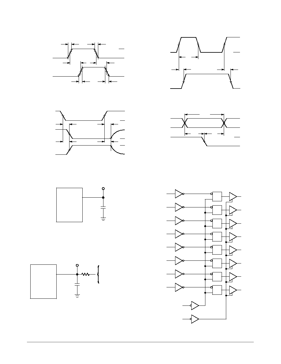
SWITCHING WAVEFORMS
VCC
GND
tf
tr
INPUT D
Q
10%
50%
90%
10%
50%
90%
tTLH
tPLH
tPHL
tTHL
OUTPUT
ENABLE
Q
Q
50%
50%
1.3 V
90%
10%
tPZL
tPLZ
tPZH
tPHZ
3.0 V
GND
HIGH
IMPEDANCE
VOL
VOH
HIGH
IMPEDANCE
*Includes all probe and jig capacitance
CL*
TEST POINT
DEVICE
UNDER
TEST
OUTPUT
*Includes all probe and jig capacitance
CL*
TEST POINT
DEVICE
UNDER
TEST
OUTPUT
CONNECT TO VCC WHEN
TESTING tPLZ AND tPZL.
CONNECT TO GND WHEN
TESTING tPHZ AND tPZH.
1 k
Figure 1.
Figure 2.
Figure 3.
Figure 4.
VCC
GND
50%
50%
LATCH
ENABLE
tPLH
tPHL
Q
tw
Figure 5. Test Circuit
Figure 6. Test Circuit
EXPANDED LOGIC DIAGRAM
D
LE
Q
D0
2
19
Q0
D
LE
Q
D1
3
18
Q1
D
LE
Q
D2
4
17
Q2
D
LE
Q
D3
5
16
Q3
D
LE
Q
D4
6
15
Q4
D
LE
Q
D5
7
14
Q5
D
LE
Q
D6
8
13
Q6
D
LE
Q
D7
9
12
Q7
LATCH ENABLE
OUTPUT ENABLE
11
1
VCC
GND
VCC
GND
50%
50%
VALID
tSU
th
INPUT D
LATCH
ENABLE
MC74HC573A
http://onsemi.com
7
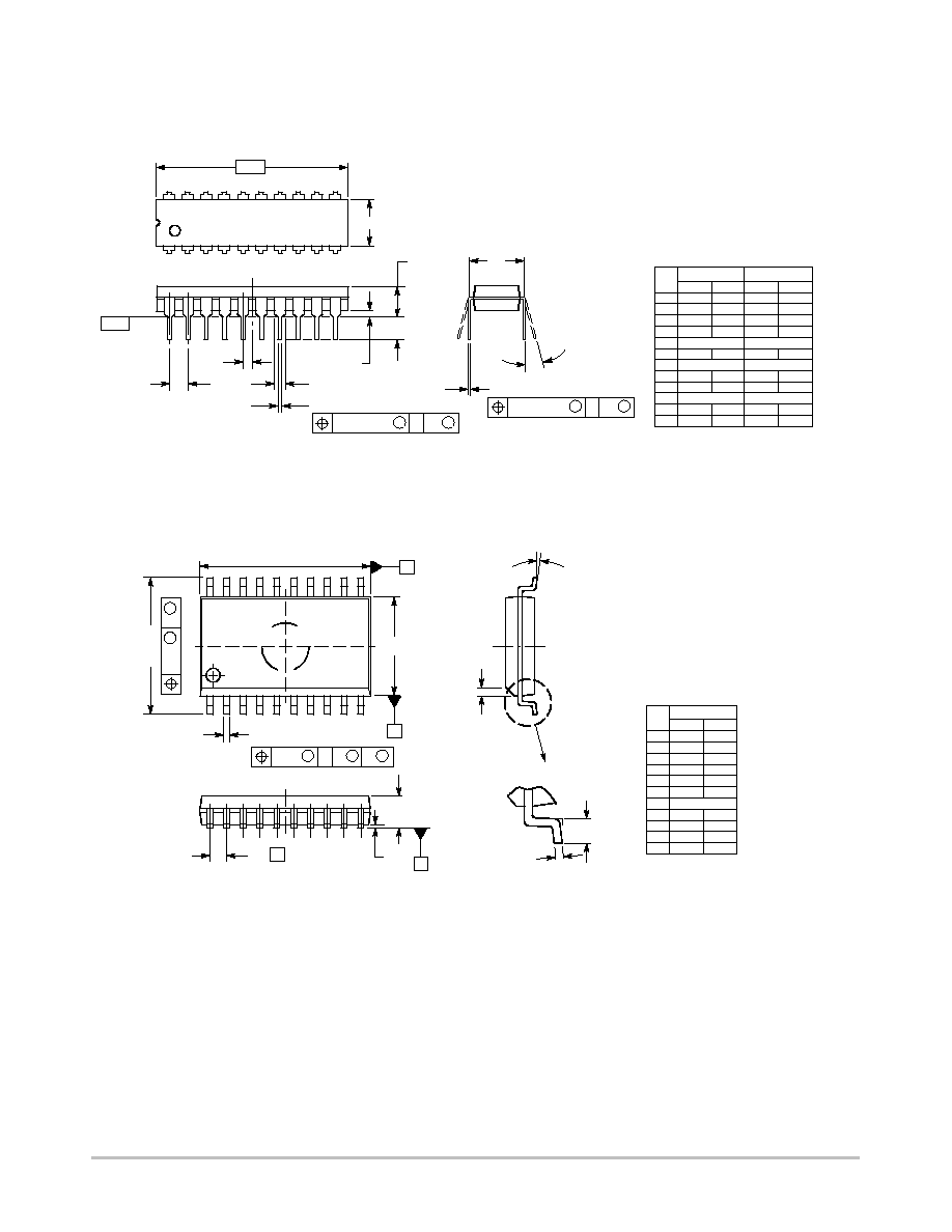
PACKAGE DIMENSIONS
SO≠20
DW SUFFIX
CASE 751D≠05
ISSUE F
PDIP≠20
N SUFFIX
PLASTIC DIP PACKAGE
CASE 738≠03
ISSUE E
NOTES:
1. DIMENSIONING AND TOLERANCING PER ANSI
Y14.5M, 1982.
2. CONTROLLING DIMENSION: INCH.
3. DIMENSION L TO CENTER OF LEAD WHEN
FORMED PARALLEL.
4. DIMENSION B DOES NOT INCLUDE MOLD
FLASH.
M
L
J
20 PL
M
B
M
0.25 (0.010)
T
DIM
MIN
MAX
MIN
MAX
MILLIMETERS
INCHES
A
25.66
27.17
1.010
1.070
B
6.10
6.60
0.240
0.260
C
3.81
4.57
0.150
0.180
D
0.39
0.55
0.015
0.022
G
2.54 BSC
0.100 BSC
J
0.21
0.38
0.008
0.015
K
2.80
3.55
0.110
0.140
L
7.62 BSC
0.300 BSC
M
0
15
0
15
N
0.51
1.01
0.020
0.040
_
_
_
_
E
1.27
1.77
0.050
0.070
1
11
10
20
≠A≠
SEATING
PLANE
K
N
F
G
D
20 PL
≠T≠
M
A
M
0.25 (0.010)
T
E
B
C
F
1.27 BSC
0.050 BSC
20
1
11
10
B
20X
H
10X
C
L
18X
A1
A
SEATING
PLANE
q
h
X 45
_
E
D
M
0.25
M
B
M
0.25
S
A
S
B
T
e
T
B
A
DIM
MIN
MAX
MILLIMETERS
A
2.35
2.65
A1
0.10
0.25
B
0.35
0.49
C
0.23
0.32
D
12.65
12.95
E
7.40
7.60
e
1.27 BSC
H
10.05
10.55
h
0.25
0.75
L
0.50
0.90
q
0
7
NOTES:
1. DIMENSIONS ARE IN MILLIMETERS.
2. INTERPRET DIMENSIONS AND TOLERANCES
PER ASME Y14.5M, 1994.
3. DIMENSIONS D AND E DO NOT INCLUDE MOLD
PROTRUSION.
4. MAXIMUM MOLD PROTRUSION 0.15 PER SIDE.
5. DIMENSION B DOES NOT INCLUDE DAMBAR
PROTRUSION. ALLOWABLE PROTRUSION SHALL
BE 0.13 TOTAL IN EXCESS OF B DIMENSION AT
MAXIMUM MATERIAL CONDITION.
_
_
MC74HC573A
http://onsemi.com
8
PACKAGE DIMENSIONS
TSSOP≠20
DT SUFFIX
CASE 948E≠02
ISSUE A
DIM
A
MIN
MAX
MIN
MAX
INCHES
6.60
0.260
MILLIMETERS
B
4.30
4.50
0.169
0.177
C
1.20
0.047
D
0.05
0.15
0.002
0.006
F
0.50
0.75
0.020
0.030
G
0.65 BSC
0.026 BSC
H
0.27
0.37
0.011
0.015
J
0.09
0.20
0.004
0.008
J1
0.09
0.16
0.004
0.006
K
0.19
0.30
0.007
0.012
K1
0.19
0.25
0.007
0.010
L
6.40 BSC
0.252 BSC
M
0 8 0 8
_
_
_
_
NOTES:
1.
DIMENSIONING AND TOLERANCING PER ANSI
Y14.5M, 1982.
2.
CONTROLLING DIMENSION: MILLIMETER.
3.
DIMENSION A DOES NOT INCLUDE MOLD
FLASH, PROTRUSIONS OR GATE BURRS. MOLD
FLASH OR GATE BURRS SHALL NOT EXCEED
0.15 (0.006) PER SIDE.
4.
DIMENSION B DOES NOT INCLUDE
INTERLEAD FLASH OR PROTRUSION.
INTERLEAD FLASH OR PROTRUSION SHALL NOT
EXCEED 0.25 (0.010) PER SIDE.
5.
DIMENSION K DOES NOT INCLUDE DAMBAR
PROTRUSION. ALLOWABLE DAMBAR
PROTRUSION SHALL BE 0.08 (0.003) TOTAL IN
EXCESS OF THE K DIMENSION AT MAXIMUM
MATERIAL CONDITION.
6.
TERMINAL NUMBERS ARE SHOWN FOR
REFERENCE ONLY.
7.
DIMENSION A AND B ARE TO BE
DETERMINED AT DATUM PLANE ≠W≠.
ÕÕÕÕ
ÕÕÕÕ
ÕÕÕÕ
1
10
11
20
PIN 1
IDENT
A
B
≠T≠
0.100 (0.004)
C
D
G
H
SECTION N≠N
K
K1
J J1
N
N
M
F
≠W≠
SEATING
PLANE
≠V≠
≠U≠
S
U
M
0.10 (0.004)
V
S
T
20X REF
K
L
L/2
2X
S
U
0.15 (0.006) T
DETAIL E
0.25 (0.010)
DETAIL E
6.40
0.252
≠≠≠
≠≠≠
S
U
0.15 (0.006) T
ON Semiconductor and are trademarks of Semiconductor Components Industries, LLC (SCILLC). SCILLC reserves the right to make changes
without further notice to any products herein. SCILLC makes no warranty, representation or guarantee regarding the suitability of its products for any particular
purpose, nor does SCILLC assume any liability arising out of the application or use of any product or circuit, and specifically disclaims any and all liability,
including without limitation special, consequential or incidental damages. "Typical" parameters which may be provided in SCILLC data sheets and/or
specifications can and do vary in different applications and actual performance may vary over time. All operating parameters, including "Typicals" must be
validated for each customer application by customer's technical experts. SCILLC does not convey any license under its patent rights nor the rights of others.
SCILLC products are not designed, intended, or authorized for use as components in systems intended for surgical implant into the body, or other applications
intended to support or sustain life, or for any other application in which the failure of the SCILLC product could create a situation where personal injury or
death may occur. Should Buyer purchase or use SCILLC products for any such unintended or unauthorized application, Buyer shall indemnify and hold
SCILLC and its officers, employees, subsidiaries, affiliates, and distributors harmless against all claims, costs, damages, and expenses, and reasonable
attorney fees arising out of, directly or indirectly, any claim of personal injury or death associated with such unintended or unauthorized use, even if such claim
alleges that SCILLC was negligent regarding the design or manufacture of the part. SCILLC is an Equal Opportunity/Affirmative Action Employer.
PUBLICATION ORDERING INFORMATION
CENTRAL/SOUTH AMERICA:
Spanish Phone: 303≠308≠7143 (Mon≠Fri 8:00am to 5:00pm MST)
Email: ONlit≠spanish@hibbertco.com
ASIA/PACIFIC: LDC for ON Semiconductor ≠ Asia Support
Phone: 303≠675≠2121 (Tue≠Fri 9:00am to 1:00pm, Hong Kong Time)
Toll Free from Hong Kong & Singapore:
001≠800≠4422≠3781
Email: ONlit≠asia@hibbertco.com
JAPAN: ON Semiconductor, Japan Customer Focus Center
4≠32≠1 Nishi≠Gotanda, Shinagawa≠ku, Tokyo, Japan 141≠8549
Phone: 81≠3≠5740≠2745
Email: r14525@onsemi.com
ON Semiconductor Website: http://onsemi.com
For additional information, please contact your local
Sales Representative.
MC74HC573A/D
NORTH AMERICA Literature Fulfillment:
Literature Distribution Center for ON Semiconductor
P.O. Box 5163, Denver, Colorado 80217 USA
Phone: 303≠675≠2175 or 800≠344≠3860 Toll Free USA/Canada
Fax: 303≠675≠2176 or 800≠344≠3867 Toll Free USA/Canada
Email: ONlit@hibbertco.com
Fax Response Line: 303≠675≠2167 or 800≠344≠3810 Toll Free USA/Canada
N. American Technical Support: 800≠282≠9855 Toll Free USA/Canada
EUROPE: LDC for ON Semiconductor ≠ European Support
German Phone: (+1) 303≠308≠7140 (M≠F 1:00pm to 5:00pm Munich Time)
Email: ONlit≠german@hibbertco.com
French Phone: (+1) 303≠308≠7141 (M≠F 1:00pm to 5:00pm Toulouse Time)
Email: ONlit≠french@hibbertco.com
English Phone: (+1) 303≠308≠7142 (M≠F 12:00pm to 5:00pm UK Time)
Email: ONlit@hibbertco.com
EUROPEAN TOLL≠FREE ACCESS*: 00≠800≠4422≠3781
*Available from Germany, France, Italy, England, Ireland