
⌐
Semiconductor Components Industries, LLC, 2000
March, 2000 ¡ Rev. 8
1
Publication Order Number:
MC74HC595A/D
MC74HC595A
8-Bit Serial-Input/Serial or
Parallel-Output Shift
Register with Latched
3-State Outputs
High¡Performance Silicon¡Gate CMOS
The MC74HC595A consists of an 8¡bit shift register and an 8¡bit
D¡type latch with three¡state parallel outputs. The shift register
accepts serial data and provides a serial output. The shift register also
provides parallel data to the 8¡bit latch. The shift register and latch
have independent clock inputs. This device also has an asynchronous
reset for the shift register.
The HC595A directly interfaces with the SPI serial data port on
CMOS MPUs and MCUs.
╖
Output Drive Capability: 15 LSTTL Loads
╖
Outputs Directly Interface to CMOS, NMOS, and TTL
╖
Operating Voltage Range: 2.0 to 6.0 V
╖
Low Input Current: 1.0
╡
A
╖
High Noise Immunity Characteristic of CMOS Devices
╖
In Compliance with the Requirements Defined by JEDEC Standard
No. 7A
╖
Chip Complexity: 328 FETs or 82 Equivalent Gates
╖
Improvements over HC595
-- Improved Propagation Delays
-- 50% Lower Quiescent Power
-- Improved Input Noise and Latchup Immunity
LOGIC DIAGRAM
SERIAL
DATA
INPUT
14
11
10
12
13
SHIFT
CLOCK
RESET
LATCH
CLOCK
OUTPUT
ENABLE
SHIFT
REGISTER
LATCH
15
1
2
3
4
5
6
7
9
QA
QB
QC
QD
QE
QF
QG
QH
SQH
A
VCC = PIN 16
GND = PIN 8
PARALLEL
DATA
OUTPUTS
SERIAL
DATA
OUTPUT
SO¡16
D SUFFIX
CASE 751B
http://onsemi.com
TSSOP¡16
DT SUFFIX
CASE 948F
1
16
PDIP¡16
N SUFFIX
CASE 648
1
16
1
16
MARKING
DIAGRAMS
1
16
MC74HC595AN
AWLYYWW
1
16
HC595A
AWLYWW
A
= Assembly Location
WL = Wafer Lot
YY = Year
WW = Work Week
HC
595A
ALYW
1
16
Device
Package
Shipping
ORDERING INFORMATION
MC74HC595AN
PDIP¡16
2000 / Box
MC74HC595AD
SOIC¡16
48 / Rail
MC74HC595ADR2
SOIC¡16
2500 / Reel
MC74HC595ADT
TSSOP¡16
96 / Rail
MC74HC595ADTR2
TSSOP¡16
2500 / Reel
PIN ASSIGNMENT
13
14
15
16
9
10
11
12
5
4
3
2
1
8
7
6
LATCH CLOCK
OUTPUT ENABLE
A
QA
VCC
SQH
RESET
SHIFT CLOCK
QE
QD
QC
QB
GND
QH
QG
QF

MC74HC595A
http://onsemi.com
2
╬╬╬╬╬╬╬╬╬╬╬╬╬╬╬╬╬╬╬╬╬╬╬
╬╬╬╬╬╬╬╬╬╬╬╬╬╬╬╬╬╬╬╬╬╬╬
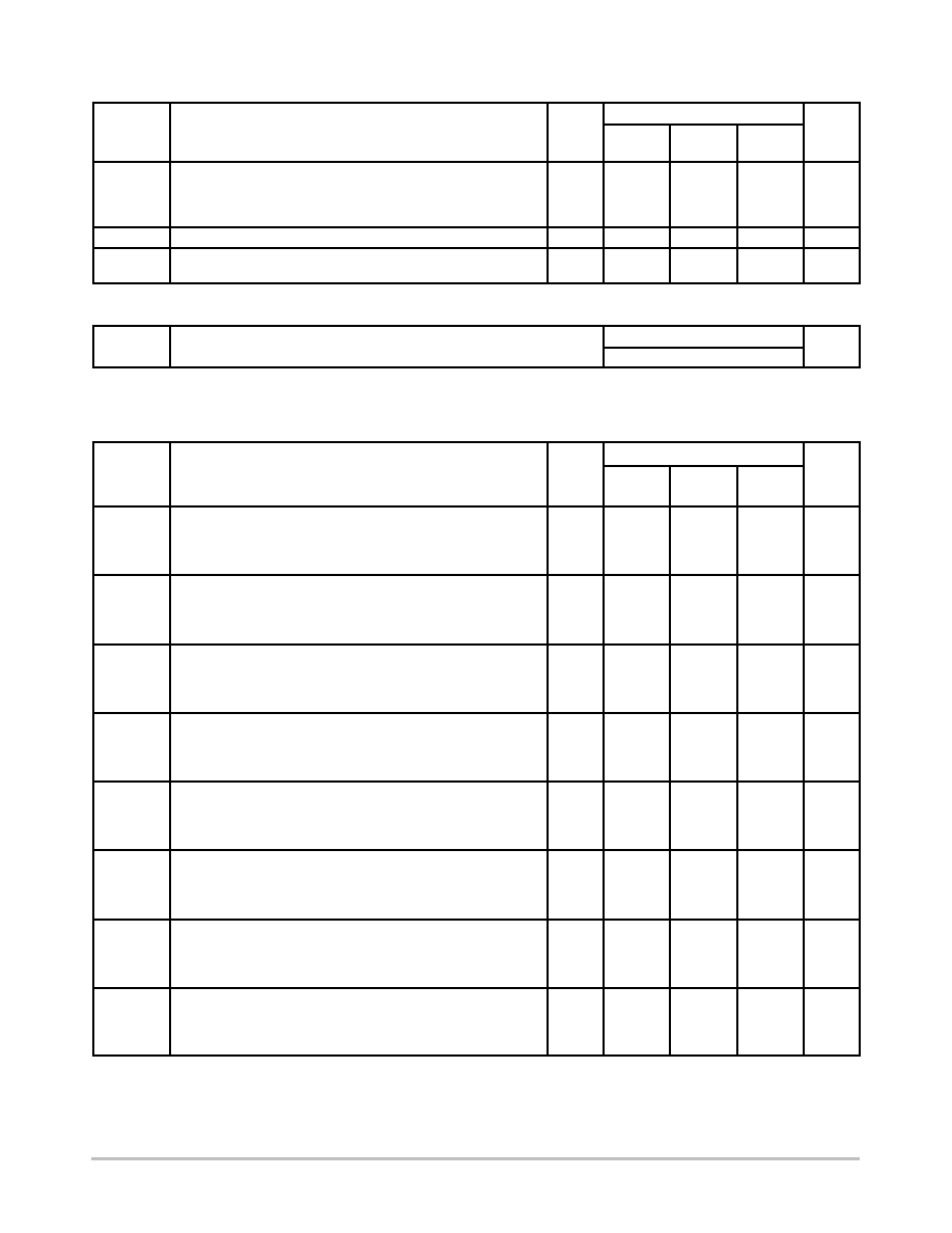
MAXIMUM RATINGS*
╬╬╬╬
╬╬╬╬
Symbol
╬╬╬╬╬╬╬╬╬╬╬╬╬╬
╬╬╬╬╬╬╬╬╬╬╬╬╬╬
Parameter
╬╬╬╬╬
╬╬╬╬╬
Value
╬╬╬
╬╬╬
Unit
╬╬╬╬
╬╬╬╬
VCC
╬╬╬╬╬╬╬╬╬╬╬╬╬╬
╬╬╬╬╬╬╬╬╬╬╬╬╬╬
DC Supply Voltage (Referenced to GND)
╬╬╬╬╬
╬╬╬╬╬
¡ 0.5 to + 7.0
╬╬╬
╬╬╬
V
╬╬╬╬
╬╬╬╬
Vin
╬╬╬╬╬╬╬╬╬╬╬╬╬╬
╬╬╬╬╬╬╬╬╬╬╬╬╬╬
DC Input Voltage (Referenced to GND)
╬╬╬╬╬
╬╬╬╬╬
¡ 0.5 to VCC + 0.5
╬╬╬
╬╬╬
V
╬╬╬╬
╬╬╬╬
Vout
╬╬╬╬╬╬╬╬╬╬╬╬╬╬
╬╬╬╬╬╬╬╬╬╬╬╬╬╬
DC Output Voltage (Referenced to GND)
╬╬╬╬╬
╬╬╬╬╬
¡ 0.5 to VCC + 0.5
╬╬╬
╬╬╬
V
╬╬╬╬
╬╬╬╬
Iin
╬╬╬╬╬╬╬╬╬╬╬╬╬╬
╬╬╬╬╬╬╬╬╬╬╬╬╬╬
DC Input Current, per Pin
╬╬╬╬╬
╬╬╬╬╬
▒
20
╬╬╬
╬╬╬
mA
╬╬╬╬
╬╬╬╬
Iout
╬╬╬╬╬╬╬╬╬╬╬╬╬╬
╬╬╬╬╬╬╬╬╬╬╬╬╬╬
DC Output Current, per Pin
╬╬╬╬╬
╬╬╬╬╬
▒
35
╬╬╬
╬╬╬
mA
╬╬╬╬
╬╬╬╬
ICC
╬╬╬╬╬╬╬╬╬╬╬╬╬╬
╬╬╬╬╬╬╬╬╬╬╬╬╬╬
DC Supply Current, VCC and GND Pins
╬╬╬╬╬
╬╬╬╬╬
▒
75
╬╬╬
╬╬╬
mA
╬╬╬╬
╬
╬╬
╬
╬╬╬╬
PD
╬╬╬╬╬╬╬╬╬╬╬╬╬╬
╬
╬╬╬╬╬╬╬╬╬╬╬╬
╬
╬╬╬╬╬╬╬╬╬╬╬╬╬╬
Power Dissipation in Still Air,
Plastic DIP
SOIC Package
TSSOP Package
╬╬╬╬╬
╬
╬╬╬
╬
╬╬╬╬╬
750
500
450
╬╬╬
╬
╬
╬
╬╬╬
mW
╬╬╬╬
╬╬╬╬
Tstg
╬╬╬╬╬╬╬╬╬╬╬╬╬╬
╬╬╬╬╬╬╬╬╬╬╬╬╬╬
Storage Temperature
╬╬╬╬╬
╬╬╬╬╬
¡ 65 to + 150
╬╬╬
╬╬╬
_
C
╬╬╬╬
╬
╬╬
╬
╬╬╬╬
TL
╬╬╬╬╬╬╬╬╬╬╬╬╬╬
╬
╬╬╬╬╬╬╬╬╬╬╬╬
╬
╬╬╬╬╬╬╬╬╬╬╬╬╬╬
Lead Temperature, 1 mm from Case for 10 Seconds
(Plastic DIP, SOIC or TSSOP Package)
╬╬╬╬╬
╬
╬╬╬
╬
╬╬╬╬╬
260
╬╬╬
╬
╬
╬
╬╬╬
_
C
*Maximum Ratings are those values beyond which damage to the device may occur.
Functional operation should be restricted to the Recommended Operating Conditions.
Derating -- Plastic DIP: ¡ 10 mW/
_
C from 65
_
to 125
_
C
SOIC Package: ¡ 7 mW/
_
C from 65
_
to 125
_
C
TSSOP Package: ¡ 6.1 mW/
_
C from 65
_
to 125
_
C
For high frequency or heavy load considerations, see Chapter 2 of the ON Semiconductor High¡Speed CMOS Data Book (DL129/D).
RECOMMENDED OPERATING CONDITIONS
╬╬╬╬
╬╬╬╬
Symbol
╬╬╬╬╬╬╬╬╬╬╬╬╬╬╬
╬╬╬╬╬╬╬╬╬╬╬╬╬╬╬
Parameter
╬╬╬
╬╬╬
Min
╬╬
╬╬
Max
╬╬╬
╬╬╬
Unit
╬╬╬╬
╬╬╬╬
VCC
╬╬╬╬╬╬╬╬╬╬╬╬╬╬╬
╬╬╬╬╬╬╬╬╬╬╬╬╬╬╬
DC Supply Voltage (Referenced to GND)
╬╬╬
╬╬╬
2.0
╬╬
╬╬
6.0
╬╬╬
╬╬╬
V
╬╬╬╬
╬
╬╬
╬
╬╬╬╬
Vin, Vout
╬╬╬╬╬╬╬╬╬╬╬╬╬╬╬
╬
╬╬╬╬╬╬╬╬╬╬╬╬╬
╬
╬╬╬╬╬╬╬╬╬╬╬╬╬╬╬
DC Input Voltage, Output Voltage
(Referenced to GND)
╬╬╬
╬
╬
╬
╬╬╬
0
╬╬
╬╬
╬╬
VCC
╬╬╬
╬
╬
╬
╬╬╬
V
╬╬╬╬
╬╬╬╬
TA
╬╬╬╬╬╬╬╬╬╬╬╬╬╬╬
╬╬╬╬╬╬╬╬╬╬╬╬╬╬╬
Operating Temperature, All Package Types
╬╬╬
╬╬╬
¡ 55
╬╬
╬╬
+ 125
╬╬╬
╬╬╬
_
C
╬╬╬╬
╬
╬╬
╬
╬╬╬╬
tr, tf
╬╬╬╬╬╬╬╬╬╬╬╬╬╬╬
╬
╬╬╬╬╬╬╬╬╬╬╬╬╬
╬
╬╬╬╬╬╬╬╬╬╬╬╬╬╬╬
Input Rise and Fall Time
VCC = 2.0 V
(Figure 1)
VCC = 4.5 V
VCC = 6.0 V
╬╬╬
╬
╬
╬
╬╬╬
0
0
0
╬╬
╬╬
╬╬
1000
500
400
╬╬╬
╬
╬
╬
╬╬╬
ns
DC ELECTRICAL CHARACTERISTICS
(Voltages Referenced to GND)
╬╬╬╬
╬╬╬╬
╬╬╬╬╬╬╬╬╬
╬╬╬╬╬╬╬╬╬
╬╬╬╬╬╬╬╬╬
╬╬╬╬╬╬╬╬╬
╬╬╬╬
╬╬╬╬
╬╬╬╬╬╬╬╬╬
╬╬╬╬╬╬╬╬╬
Guaranteed Limit
╬╬╬
╬╬╬
╬╬╬╬
╬
╬╬
╬
╬╬╬╬
Symbol
╬╬╬╬╬╬╬╬╬
╬
╬╬╬╬╬╬╬
╬
╬╬╬╬╬╬╬╬╬
Parameter
╬╬╬╬╬╬╬╬╬
╬
╬╬╬╬╬╬╬
╬
╬╬╬╬╬╬╬╬╬
Test Conditions
╬╬╬╬
╬
╬╬
╬
╬╬╬╬
VCC
V
╬╬╬╬
╬
╬╬
╬
╬╬╬╬
¡ 55 to
25
_
C
╬╬╬
╬
╬
╬
╬╬╬
v
85
_
C
╬╬╬╬
╬
╬╬
╬
╬╬╬╬
v
125
_
C
╬╬╬
╬
╬
╬
╬╬╬
Unit
╬╬╬╬
╬
╬╬
╬
╬
╬╬
╬
╬╬╬╬
VIH
╬╬╬╬╬╬╬╬╬
╬
╬╬╬╬╬╬╬
╬
╬
╬╬╬╬╬╬╬
╬
╬╬╬╬╬╬╬╬╬
Minimum High¡Level Input
Voltage
╬╬╬╬╬╬╬╬╬
╬
╬╬╬╬╬╬╬
╬
╬
╬╬╬╬╬╬╬
╬
╬╬╬╬╬╬╬╬╬
Vout = 0.1 V or VCC ¡ 0.1 V
|Iout|
v
20
╡
A
╬╬╬╬
╬
╬╬
╬
╬
╬╬
╬
╬╬╬╬
2.0
3.0
4.5
6.0
╬╬╬╬
╬
╬╬
╬
╬
╬╬
╬
╬╬╬╬
1.5
2.1
3.15
4.2
╬╬╬
╬
╬
╬
╬
╬
╬
╬╬╬
1.5
2.1
3.15
4.2
╬╬╬╬
╬
╬╬
╬
╬
╬╬
╬
╬╬╬╬
1.5
2.1
3.15
4.2
╬╬╬
╬
╬
╬
╬
╬
╬
╬╬╬
V
╬╬╬╬
╬
╬╬
╬
╬
╬╬
╬
╬╬╬╬
VIL
╬╬╬╬╬╬╬╬╬
╬
╬╬╬╬╬╬╬
╬
╬
╬╬╬╬╬╬╬
╬
╬╬╬╬╬╬╬╬╬
Maximum Low¡Level Input
Voltage
╬╬╬╬╬╬╬╬╬
╬
╬╬╬╬╬╬╬
╬
╬
╬╬╬╬╬╬╬
╬
╬╬╬╬╬╬╬╬╬
Vout = 0.1 V or VCC ¡ 0.1 V
|Iout|
v
20
╡
A
╬╬╬╬
╬
╬╬
╬
╬
╬╬
╬
╬╬╬╬
2.0
3.0
4.5
6.0
╬╬╬╬
╬
╬╬
╬
╬
╬╬
╬
╬╬╬╬
0.5
0.9
1.35
1.8
╬╬╬
╬
╬
╬
╬
╬
╬
╬╬╬
0.5
0.9
1.35
1.8
╬╬╬╬
╬
╬╬
╬
╬
╬╬
╬
╬╬╬╬
0.5
0.9
1.35
1.8
╬╬╬
╬
╬
╬
╬
╬
╬
╬╬╬
V
╬╬╬╬
╬
╬╬
╬
╬╬╬╬
VOH
╬╬╬╬╬╬╬╬╬
╬
╬╬╬╬╬╬╬
╬
╬╬╬╬╬╬╬╬╬
Minimum High¡Level Output
Voltage, QA ¡ QH
╬╬╬╬╬╬╬╬╬
╬
╬╬╬╬╬╬╬
╬
╬╬╬╬╬╬╬╬╬
Vin = VIH or VIL
|Iout|
v
20
╡
A
╬╬╬╬
╬
╬╬
╬
╬╬╬╬
2.0
4.5
6.0
╬╬╬╬
╬
╬╬
╬
╬╬╬╬
1.9
4.4
5.9
╬╬╬
╬
╬
╬
╬╬╬
1.9
4.4
5.9
╬╬╬╬
╬
╬╬
╬
╬╬╬╬
1.9
4.4
5.9
╬╬╬
╬
╬
╬
╬╬╬
V
╬╬╬╬
╬
╬╬
╬
╬╬╬╬
╬╬╬╬╬╬╬╬╬
╬
╬╬╬╬╬╬╬
╬
╬╬╬╬╬╬╬╬╬
╬╬╬╬╬╬╬╬╬
╬
╬╬╬╬╬╬╬
╬
╬╬╬╬╬╬╬╬╬
Vin = VIH or VIL |Iout|
v
2.4 mA
|Iout|
v
6.0 mA
|Iout|
v
7.8 mA
╬╬╬╬
╬
╬╬
╬
╬╬╬╬
3.0
4.5
6.0
╬╬╬╬
╬
╬╬
╬
╬╬╬╬
2.48
3.98
5.48
╬╬╬
╬
╬
╬
╬╬╬
2.34
3.84
5.34
╬╬╬╬
╬
╬╬
╬
╬╬╬╬
2.2
3.7
5.2
╬╬╬
╬
╬
╬
╬╬╬
╬╬╬╬
╬
╬╬
╬
╬
╬╬
╬
╬╬╬╬
VOL
╬╬╬╬╬╬╬╬╬
╬
╬╬╬╬╬╬╬
╬
╬
╬╬╬╬╬╬╬
╬
╬╬╬╬╬╬╬╬╬
Maximum Low¡Level Output
Voltage, QA ¡ QH
╬╬╬╬╬╬╬╬╬
╬
╬╬╬╬╬╬╬
╬
╬
╬╬╬╬╬╬╬
╬
╬╬╬╬╬╬╬╬╬
Vin = VIH or VIL
|Iout|
v
20
╡
A
╬╬╬╬
╬
╬╬
╬
╬
╬╬
╬
╬╬╬╬
2.0
4.5
6.0
╬╬╬╬
╬
╬╬
╬
╬
╬╬
╬
╬╬╬╬
0.1
0.1
0.1
╬╬╬
╬
╬
╬
╬
╬
╬
╬╬╬
0.1
0.1
0.1
╬╬╬╬
╬
╬╬
╬
╬
╬╬
╬
╬╬╬╬
0.1
0.1
0.1
╬╬╬
╬
╬
╬
╬
╬
╬
╬╬╬
V
╬╬╬╬
╬
╬╬
╬
╬╬╬╬
╬╬╬╬╬╬╬╬╬
╬
╬╬╬╬╬╬╬
╬
╬╬╬╬╬╬╬╬╬
╬╬╬╬╬╬╬╬╬
╬
╬╬╬╬╬╬╬
╬
╬╬╬╬╬╬╬╬╬
Vin = VIH or VIL |Iout|
v
2.4 mA
|Iout|
v
6.0 mA
|Iout|
v
7.8 mA
╬╬╬╬
╬
╬╬
╬
╬╬╬╬
3.0
4.5
6.0
╬╬╬╬
╬
╬╬
╬
╬╬╬╬
0.26
0.26
0.26
╬╬╬
╬
╬
╬
╬╬╬
0.33
0.33
0.33
╬╬╬╬
╬
╬╬
╬
╬╬╬╬
0.4
0.4
0.4
╬╬╬
╬
╬
╬
╬╬╬
This device contains protection
circuitry to guard against damage
due to high static voltages or electric
fields. However, precautions must
be taken to avoid applications of any
voltage higher than maximum rated
voltages to this high¡impedance cir-
cuit. For proper operation, Vin and
Vout should be constrained to the
range GND
v
(Vin or Vout)
v
VCC.
Unused inputs must always be
tied to an appropriate logic voltage
level (e.g., either GND or VCC).
Unused outputs must be left open.

MC74HC595A
http://onsemi.com
3
DC ELECTRICAL CHARACTERISTICS
(Voltages Referenced to GND)
╬╬╬
╬╬╬
Unit
╬╬╬╬╬╬╬╬╬
╬╬╬╬╬╬╬╬╬
Guaranteed Limit
╬╬╬╬
╬╬╬╬
VCC
V
╬╬╬╬╬╬╬╬╬
╬╬╬╬╬╬╬╬╬
Test Conditions
╬╬╬╬╬╬╬╬╬
╬╬╬╬╬╬╬╬╬
Parameter
╬╬╬╬
╬╬╬╬
Symbol
╬╬╬
╬╬╬
Unit
╬╬╬╬
╬╬╬╬
v
125
_
C
╬╬╬
╬╬╬
v
85
_
C
╬╬╬╬
╬╬╬╬
¡ 55 to
25
_
C
╬╬╬╬
╬╬╬╬
VCC
V
╬╬╬╬╬╬╬╬╬
╬╬╬╬╬╬╬╬╬
Test Conditions
╬╬╬╬╬╬╬╬╬
╬╬╬╬╬╬╬╬╬
Parameter
╬╬╬╬
╬╬╬╬
Symbol
╬╬╬╬
╬
╬╬
╬
╬
╬╬
╬
╬╬╬╬
VOH
╬╬╬╬╬╬╬╬╬
╬
╬╬╬╬╬╬╬
╬
╬
╬╬╬╬╬╬╬
╬
╬╬╬╬╬╬╬╬╬
Minimum High¡Level Output
Voltage, SQH
╬╬╬╬╬╬╬╬╬
╬
╬╬╬╬╬╬╬
╬
╬
╬╬╬╬╬╬╬
╬
╬╬╬╬╬╬╬╬╬
Vin = VIH or VIL
IIoutI
v
20
╡
A
╬╬╬╬
╬
╬╬
╬
╬
╬╬
╬
╬╬╬╬
2.0
4.5
6.0
╬╬╬╬
╬
╬╬
╬
╬
╬╬
╬
╬╬╬╬
1.9
4.4
5.9
╬╬╬
╬
╬
╬
╬
╬
╬
╬╬╬
1.9
4.4
5.9
╬╬╬╬
╬
╬╬
╬
╬
╬╬
╬
╬╬╬╬
1.9
4.4
5.9
╬╬╬
╬
╬
╬
╬
╬
╬
╬╬╬
V
╬╬╬╬
╬
╬╬
╬
╬╬╬╬
╬╬╬╬╬╬╬╬╬
╬
╬╬╬╬╬╬╬
╬
╬╬╬╬╬╬╬╬╬
╬╬╬╬╬╬╬╬╬
╬
╬╬╬╬╬╬╬
╬
╬╬╬╬╬╬╬╬╬
Vin = VIH or VIL |Iout|
v
2.4 mA
IIoutI
v
4.0 mA
IIoutI
v
5.2 mA
╬╬╬╬
╬
╬╬
╬
╬╬╬╬
3.0
4.5
6.0
╬╬╬╬
╬
╬╬
╬
╬╬╬╬
2.98
3.98
5.48
╬╬╬
╬
╬
╬
╬╬╬
2.34
3.84
5.34
╬╬╬╬
╬
╬╬
╬
╬╬╬╬
2.2
3.7
5.2
╬╬╬
╬
╬
╬
╬╬╬
╬╬╬╬
╬
╬╬
╬
╬╬╬╬
VOL
╬╬╬╬╬╬╬╬╬
╬
╬╬╬╬╬╬╬
╬
╬╬╬╬╬╬╬╬╬
Maximum Low¡Level Output
Voltage, SQH
╬╬╬╬╬╬╬╬╬
╬
╬╬╬╬╬╬╬
╬
╬╬╬╬╬╬╬╬╬
Vin = VIH or VIL
IIoutI
v
20
╡
A
╬╬╬╬
╬
╬╬
╬
╬╬╬╬
2.0
4.5
6.0
╬╬╬╬
╬
╬╬
╬
╬╬╬╬
0.1
0.1
0.1
╬╬╬
╬
╬
╬
╬╬╬
0.1
0.1
0.1
╬╬╬╬
╬
╬╬
╬
╬╬╬╬
0.1
0.1
0.1
╬╬╬
╬
╬
╬
╬╬╬
V
╬╬╬╬
╬
╬╬
╬
╬╬╬╬
╬╬╬╬╬╬╬╬╬
╬
╬╬╬╬╬╬╬
╬
╬╬╬╬╬╬╬╬╬
╬╬╬╬╬╬╬╬╬
╬
╬╬╬╬╬╬╬
╬
╬╬╬╬╬╬╬╬╬
Vin = VIH or VIL |Iout|
v
2.4 mA
IIoutI
v
4.0 mA
IIoutI
v
5.2 mA
╬╬╬╬
╬
╬╬
╬
╬╬╬╬
3.0
4.5
6.0
╬╬╬╬
╬
╬╬
╬
╬╬╬╬
0.26
0.26
0.26
╬╬╬
╬
╬
╬
╬╬╬
0.33
0.33
0.33
╬╬╬╬
╬
╬╬
╬
╬╬╬╬
0.4
0.4
0.4
╬╬╬
╬
╬
╬
╬╬╬
╬╬╬╬
╬
╬╬
╬
╬╬╬╬
Iin
╬╬╬╬╬╬╬╬╬
╬
╬╬╬╬╬╬╬
╬
╬╬╬╬╬╬╬╬╬
Maximum Input Leakage
Current
╬╬╬╬╬╬╬╬╬
╬
╬╬╬╬╬╬╬
╬
╬╬╬╬╬╬╬╬╬
Vin = VCC or GND
╬╬╬╬
╬
╬╬
╬
╬╬╬╬
6.0
╬╬╬╬
╬
╬╬
╬
╬╬╬╬
▒
0.1
╬╬╬
╬
╬
╬
╬╬╬
▒
1.0
╬╬╬╬
╬
╬╬
╬
╬╬╬╬
▒
1.0
╬╬╬
╬
╬
╬
╬╬╬
╡
A
╬╬╬╬
╬
╬╬
╬
╬╬╬╬
IOZ
╬╬╬╬╬╬╬╬╬
╬
╬╬╬╬╬╬╬
╬
╬╬╬╬╬╬╬╬╬
Maximum Three¡State
Leakage
Current, QA ¡ QH
╬╬╬╬╬╬╬╬╬
╬
╬╬╬╬╬╬╬
╬
╬╬╬╬╬╬╬╬╬
Output in High¡Impedance State
Vin = VIL or VIH
Vout = VCC or GND
╬╬╬╬
╬
╬╬
╬
╬╬╬╬
6.0
╬╬╬╬
╬
╬╬
╬
╬╬╬╬
▒
0.5
╬╬╬
╬
╬
╬
╬╬╬
▒
5.0
╬╬╬╬
╬
╬╬
╬
╬╬╬╬
▒
10
╬╬╬
╬
╬
╬
╬╬╬
╡
A
╬╬╬╬
╬
╬╬
╬
╬╬╬╬
ICC
╬╬╬╬╬╬╬╬╬
╬
╬╬╬╬╬╬╬
╬
╬╬╬╬╬╬╬╬╬
Maximum Quiescent Supply
Current (per Package)
╬╬╬╬╬╬╬╬╬
╬
╬╬╬╬╬╬╬
╬
╬╬╬╬╬╬╬╬╬
Vin = VCC or GND
lout = 0
╡
A
╬╬╬╬
╬
╬╬
╬
╬╬╬╬
6.0
╬╬╬╬
╬
╬╬
╬
╬╬╬╬
4.0
╬╬╬
╬
╬
╬
╬╬╬
40
╬╬╬╬
╬
╬╬
╬
╬╬╬╬
160
╬╬╬
╬
╬
╬
╬╬╬
╡
A
NOTE: Information on typical parametric values can be found in Chapter 2 of the ON Semiconductor High¡Speed CMOS Data Book
(DL129/D).
AC ELECTRICAL CHARACTERISTICS
(CL = 50 pF, Input tr = tf = 6.0 ns)
╬╬╬╬╬
╬╬╬╬╬╬╬╬╬╬╬╬╬╬╬╬
╬╬╬╬
╬╬╬╬╬╬╬╬╬
Guaranteed Limit
╬╬╬
╬╬╬╬╬
╬
╬╬╬
╬
╬╬╬╬╬
Symbol
╬╬╬╬╬╬╬╬╬╬╬╬╬╬╬╬
╬
╬╬╬╬╬╬╬╬╬╬╬╬╬╬
╬
╬╬╬╬╬╬╬╬╬╬╬╬╬╬╬╬
Parameter
╬╬╬╬
╬
╬╬
╬
╬╬╬╬
VCC
V
╬╬╬╬
╬
╬╬
╬
╬╬╬╬
¡ 55 to
25
_
C
╬╬╬
╬
╬
╬
╬╬╬
v
85
_
C
╬╬╬╬
╬
╬╬
╬
╬╬╬╬
v
125
_
C
╬╬╬
╬
╬
╬
╬╬╬
Unit
╬╬╬╬╬
╬
╬╬╬
╬
╬
╬╬╬
╬
╬╬╬╬╬
fmax
╬╬╬╬╬╬╬╬╬╬╬╬╬╬╬╬
╬
╬╬╬╬╬╬╬╬╬╬╬╬╬╬
╬
╬
╬╬╬╬╬╬╬╬╬╬╬╬╬╬
╬
╬╬╬╬╬╬╬╬╬╬╬╬╬╬╬╬
Maximum Clock Frequency (50% Duty Cycle)
(Figures 1 and 7)
╬╬╬╬
╬
╬╬
╬
╬
╬╬
╬
╬╬╬╬
2.0
3.0
4.5
6.0
╬╬╬╬
╬
╬╬
╬
╬
╬╬
╬
╬╬╬╬
6.0
15
30
35
╬╬╬
╬
╬
╬
╬
╬
╬
╬╬╬
4.8
10
24
28
╬╬╬╬
╬
╬╬
╬
╬
╬╬
╬
╬╬╬╬
4.0
8.0
20
24
╬╬╬
╬
╬
╬
╬
╬
╬
╬╬╬
MHz
╬╬╬╬╬
╬
╬╬╬
╬
╬
╬╬╬
╬
tPLH,
tPHL
╬╬╬╬╬╬╬╬╬╬╬╬╬╬╬╬
╬
╬╬╬╬╬╬╬╬╬╬╬╬╬╬
╬
╬
╬╬╬╬╬╬╬╬╬╬╬╬╬╬
╬
Maximum Propagation Delay, Shift Clock to SQH
(Figures 1 and 7)
╬╬╬╬
╬
╬╬
╬
╬
╬╬
╬
2.0
3.0
4.5
6.0
╬╬╬╬
╬
╬╬
╬
╬
╬╬
╬
140
100
28
24
╬╬╬
╬
╬
╬
╬
╬
╬
175
125
35
30
╬╬╬╬
╬
╬╬
╬
╬
╬╬
╬
210
150
42
36
╬╬╬
╬
╬
╬
╬
╬
╬
ns
╬╬╬╬╬
╬
╬╬╬
╬
╬
╬╬╬
╬
╬╬╬╬╬
tPHL
╬╬╬╬╬╬╬╬╬╬╬╬╬╬╬╬
╬
╬╬╬╬╬╬╬╬╬╬╬╬╬╬
╬
╬
╬╬╬╬╬╬╬╬╬╬╬╬╬╬
╬
╬╬╬╬╬╬╬╬╬╬╬╬╬╬╬╬
Maximum Propagation Delay, Reset to SQH
(Figures 2 and 7)
╬╬╬╬
╬
╬╬
╬
╬
╬╬
╬
╬╬╬╬
2.0
3.0
4.5
6.0
╬╬╬╬
╬
╬╬
╬
╬
╬╬
╬
╬╬╬╬
145
100
29
25
╬╬╬
╬
╬
╬
╬
╬
╬
╬╬╬
180
125
36
31
╬╬╬╬
╬
╬╬
╬
╬
╬╬
╬
╬╬╬╬
220
150
44
38
╬╬╬
╬
╬
╬
╬
╬
╬
╬╬╬
ns
╬╬╬╬╬
╬
╬╬╬
╬
╬
╬╬╬
╬
╬╬╬╬╬
tPLH,
tPHL
╬╬╬╬╬╬╬╬╬╬╬╬╬╬╬╬
╬
╬╬╬╬╬╬╬╬╬╬╬╬╬╬
╬
╬
╬╬╬╬╬╬╬╬╬╬╬╬╬╬
╬
╬╬╬╬╬╬╬╬╬╬╬╬╬╬╬╬
Maximum Propagation Delay, Latch Clock to QA ¡ QH
(Figures 3 and 7)
╬╬╬╬
╬
╬╬
╬
╬
╬╬
╬
╬╬╬╬
2.0
3.0
4.5
6.0
╬╬╬╬
╬
╬╬
╬
╬
╬╬
╬
╬╬╬╬
140
100
28
24
╬╬╬
╬
╬
╬
╬
╬
╬
╬╬╬
175
125
35
30
╬╬╬╬
╬
╬╬
╬
╬
╬╬
╬
╬╬╬╬
210
150
42
36
╬╬╬
╬
╬
╬
╬
╬
╬
╬╬╬
ns
╬╬╬╬╬
╬
╬╬╬
╬
╬
╬╬╬
╬
╬╬╬╬╬
tPLZ,
tPHZ
╬╬╬╬╬╬╬╬╬╬╬╬╬╬╬╬
╬
╬╬╬╬╬╬╬╬╬╬╬╬╬╬
╬
╬
╬╬╬╬╬╬╬╬╬╬╬╬╬╬
╬
╬╬╬╬╬╬╬╬╬╬╬╬╬╬╬╬
Maximum Propagation Delay, Output Enable to QA ¡ QH
(Figures 4 and 8)
╬╬╬╬
╬
╬╬
╬
╬
╬╬
╬
╬╬╬╬
2.0
3.0
4.5
6.0
╬╬╬╬
╬
╬╬
╬
╬
╬╬
╬
╬╬╬╬
150
100
30
26
╬╬╬
╬
╬
╬
╬
╬
╬
╬╬╬
190
125
38
33
╬╬╬╬
╬
╬╬
╬
╬
╬╬
╬
╬╬╬╬
225
150
45
38
╬╬╬
╬
╬
╬
╬
╬
╬
╬╬╬
ns
╬╬╬╬╬
╬
╬╬╬
╬
╬
╬╬╬
╬
╬╬╬╬╬
tPZL,
tPZH
╬╬╬╬╬╬╬╬╬╬╬╬╬╬╬╬
╬
╬╬╬╬╬╬╬╬╬╬╬╬╬╬
╬
╬
╬╬╬╬╬╬╬╬╬╬╬╬╬╬
╬
╬╬╬╬╬╬╬╬╬╬╬╬╬╬╬╬
Maximum Propagation Delay, Output Enable to QA ¡ QH
(Figures 4 and 8)
╬╬╬╬
╬
╬╬
╬
╬
╬╬
╬
╬╬╬╬
2.0
3.0
4.5
6.0
╬╬╬╬
╬
╬╬
╬
╬
╬╬
╬
╬╬╬╬
135
90
27
23
╬╬╬
╬
╬
╬
╬
╬
╬
╬╬╬
170
110
34
29
╬╬╬╬
╬
╬╬
╬
╬
╬╬
╬
╬╬╬╬
205
130
41
35
╬╬╬
╬
╬
╬
╬
╬
╬
╬╬╬
ns
╬╬╬╬╬
╬
╬╬╬
╬
╬╬╬╬╬
tTLH,
tTHL
╬╬╬╬╬╬╬╬╬╬╬╬╬╬╬╬
╬
╬╬╬╬╬╬╬╬╬╬╬╬╬╬
╬
╬╬╬╬╬╬╬╬╬╬╬╬╬╬╬╬
Maximum Output Transition Time, QA ¡ QH
(Figures 3 and 7)
╬╬╬╬
╬
╬╬
╬
╬╬╬╬
2.0
3.0
4.5
6.0
╬╬╬╬
╬
╬╬
╬
╬╬╬╬
60
23
12
10
╬╬╬
╬
╬
╬
╬╬╬
75
27
15
13
╬╬╬╬
╬
╬╬
╬
╬╬╬╬
90
31
18
15
╬╬╬
╬
╬
╬
╬╬╬
ns
MC74HC595A
http://onsemi.com
4
AC ELECTRICAL CHARACTERISTICS
(CL = 50 pF, Input tr = tf = 6.0 ns)
╬╬╬
╬╬╬
Unit
╬╬╬╬╬╬╬╬╬
╬╬╬╬╬╬╬╬╬
Guaranteed Limit
╬╬╬╬
╬╬╬╬
VCC
V
╬╬╬╬╬╬╬╬╬╬╬╬╬╬╬╬
╬╬╬╬╬╬╬╬╬╬╬╬╬╬╬╬
Parameter
╬╬╬╬╬
╬╬╬╬╬
Symbol
╬╬╬
╬╬╬
Unit
╬╬╬╬
╬╬╬╬
v
125
_
C
╬╬╬
╬╬╬
v
85
_
C
╬╬╬╬
╬╬╬╬
¡ 55 to
25
_
C
╬╬╬╬
╬╬╬╬
VCC
V
╬╬╬╬╬╬╬╬╬╬╬╬╬╬╬╬
╬╬╬╬╬╬╬╬╬╬╬╬╬╬╬╬
Parameter
╬╬╬╬╬
╬╬╬╬╬
Symbol
╬╬╬╬╬
╬
╬╬╬
╬
╬
╬╬╬
╬
╬╬╬╬╬
tTLH,
tTHL
╬╬╬╬╬╬╬╬╬╬╬╬╬╬╬╬
╬
╬╬╬╬╬╬╬╬╬╬╬╬╬╬
╬
╬
╬╬╬╬╬╬╬╬╬╬╬╬╬╬
╬
╬╬╬╬╬╬╬╬╬╬╬╬╬╬╬╬
Maximum Output Transition Time, SQH
(Figures 1 and 7)
╬╬╬╬
╬
╬╬
╬
╬
╬╬
╬
╬╬╬╬
2.0
3.0
4.5
6.0
╬╬╬╬
╬
╬╬
╬
╬
╬╬
╬
╬╬╬╬
75
27
15
13
╬╬╬
╬
╬
╬
╬
╬
╬
╬╬╬
95
32
19
16
╬╬╬╬
╬
╬╬
╬
╬
╬╬
╬
╬╬╬╬
110
36
22
19
╬╬╬
╬
╬
╬
╬
╬
╬
╬╬╬
ns
╬╬╬╬╬
╬╬╬╬╬
Cin
╬╬╬╬╬╬╬╬╬╬╬╬╬╬╬╬
╬╬╬╬╬╬╬╬╬╬╬╬╬╬╬╬
Maximum Input Capacitance
╬╬╬╬
╬╬╬╬
--
╬╬╬╬
╬╬╬╬
10
╬╬╬
╬╬╬
10
╬╬╬╬
╬╬╬╬
10
╬╬╬
╬╬╬
pF
╬╬╬╬╬
╬╬╬╬╬
Cout
╬╬╬╬╬╬╬╬╬╬╬╬╬╬╬╬
╬╬╬╬╬╬╬╬╬╬╬╬╬╬╬╬
Maximum Three¡State Output Capacitance (Output in
High¡Impedance State), QA ¡ QH
╬╬╬╬
╬╬╬╬
--
╬╬╬╬
╬╬╬╬
15
╬╬╬
╬╬╬
15
╬╬╬╬
╬╬╬╬
15
╬╬╬
╬╬╬
pF
NOTE: For propagation delays with loads other than 50 pF, and information on typical parametric values, see Chapter 2 of the ON
Semiconductor High¡Speed CMOS Data Book (DL129/D).
Typical @ 25
░
C, VCC = 5.0 V
CPD
Power Dissipation Capacitance (Per Package)*
300
pF
* Used to determine the no¡load dynamic power consumption: PD = CPD VCC2f + ICC VCC. For load considerations, see Chapter 2 of the
ON Semiconductor High¡Speed CMOS Data Book (DL129/D).
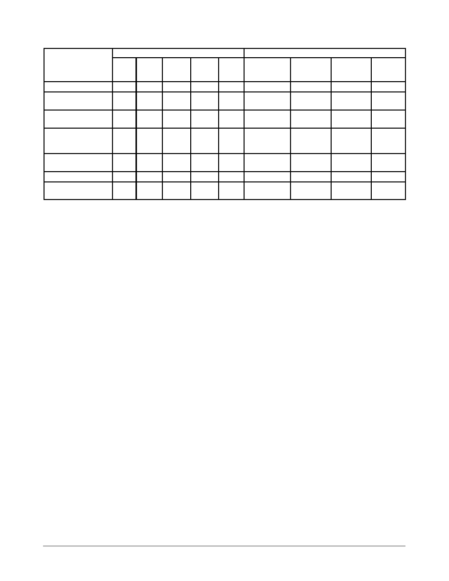
TIMING REQUIREMENTS
(Input tr = tf = 6.0 ns)
╬╬╬╬╬
╬╬╬╬╬
╬╬╬╬╬╬╬╬╬╬╬╬╬╬╬╬
╬╬╬╬╬╬╬╬╬╬╬╬╬╬╬╬
╬╬╬╬
╬╬╬╬
╬╬╬╬╬╬╬╬╬
╬╬╬╬╬╬╬╬╬
Guaranteed Limit
╬╬╬
╬╬╬
╬╬╬╬╬
╬
╬╬╬
╬
╬╬╬╬╬
Symbol
╬╬╬╬╬╬╬╬╬╬╬╬╬╬╬╬
╬
╬╬╬╬╬╬╬╬╬╬╬╬╬╬
╬
╬╬╬╬╬╬╬╬╬╬╬╬╬╬╬╬
Parameter
╬╬╬╬
╬
╬╬
╬
╬╬╬╬
VCC
V
╬╬╬╬
╬
╬╬
╬
╬╬╬╬
25
_
C to
¡ 55
_
C
╬╬╬
╬
╬
╬
╬╬╬
v
85
_
C
╬╬╬╬
╬
╬╬
╬
╬╬╬╬
v
125
_
C
╬╬╬
╬
╬
╬
╬╬╬
Unit
╬╬╬╬╬
╬
╬╬╬
╬
╬
╬╬╬
╬
╬╬╬╬╬
tsu
╬╬╬╬╬╬╬╬╬╬╬╬╬╬╬╬
╬
╬╬╬╬╬╬╬╬╬╬╬╬╬╬
╬
╬
╬╬╬╬╬╬╬╬╬╬╬╬╬╬
╬
╬╬╬╬╬╬╬╬╬╬╬╬╬╬╬╬
Minimum Setup Time, Serial Data Input A to Shift Clock
(Figure 5)
╬╬╬╬
╬
╬╬
╬
╬
╬╬
╬
╬╬╬╬
2.0
3.0
4.5
6.0
╬╬╬╬
╬
╬╬
╬
╬
╬╬
╬
╬╬╬╬
50
40
10
9.0
╬╬╬
╬
╬
╬
╬
╬
╬
╬╬╬
65
50
13
11
╬╬╬╬
╬
╬╬
╬
╬
╬╬
╬
╬╬╬╬
75
60
15
13
╬╬╬
╬
╬
╬
╬
╬
╬
╬╬╬
ns
╬╬╬╬╬
╬
╬╬╬
╬
╬╬╬╬╬
tsu
╬╬╬╬╬╬╬╬╬╬╬╬╬╬╬╬
╬
╬╬╬╬╬╬╬╬╬╬╬╬╬╬
╬
╬╬╬╬╬╬╬╬╬╬╬╬╬╬╬╬
Minimum Setup Time, Shift Clock to Latch Clock
(Figure 6)
╬╬╬╬
╬
╬╬
╬
╬╬╬╬
2.0
3.0
4.5
6.0
╬╬╬╬
╬
╬╬
╬
╬╬╬╬
75
60
15
13
╬╬╬
╬
╬
╬
╬╬╬
95
70
19
16
╬╬╬╬
╬
╬╬
╬
╬╬╬╬
110
80
22
19
╬╬╬
╬
╬
╬
╬╬╬
ns
╬╬╬╬╬
╬
╬╬╬
╬
╬
╬╬╬
╬
╬╬╬╬╬
th
╬╬╬╬╬╬╬╬╬╬╬╬╬╬╬╬
╬
╬╬╬╬╬╬╬╬╬╬╬╬╬╬
╬
╬
╬╬╬╬╬╬╬╬╬╬╬╬╬╬
╬
╬╬╬╬╬╬╬╬╬╬╬╬╬╬╬╬
Minimum Hold Time, Shift Clock to Serial Data Input A
(Figure 5)
╬╬╬╬
╬
╬╬
╬
╬
╬╬
╬
╬╬╬╬
2.0
3.0
4.5
6.0
╬╬╬╬
╬
╬╬
╬
╬
╬╬
╬
╬╬╬╬
5.0
5.0
5.0
5.0
╬╬╬
╬
╬
╬
╬
╬
╬
╬╬╬
5.0
5.0
5.0
5.0
╬╬╬╬
╬
╬╬
╬
╬
╬╬
╬
╬╬╬╬
5.0
5.0
5.0
5.0
╬╬╬
╬
╬
╬
╬
╬
╬
╬╬╬
ns
╬╬╬╬╬
╬
╬╬╬
╬
╬
╬╬╬
╬
╬╬╬╬╬
trec
╬╬╬╬╬╬╬╬╬╬╬╬╬╬╬╬
╬
╬╬╬╬╬╬╬╬╬╬╬╬╬╬
╬
╬
╬╬╬╬╬╬╬╬╬╬╬╬╬╬
╬
╬╬╬╬╬╬╬╬╬╬╬╬╬╬╬╬
Minimum Recovery Time, Reset Inactive to Shift Clock
(Figure 2)
╬╬╬╬
╬
╬╬
╬
╬
╬╬
╬
╬╬╬╬
2.0
3.0
4.5
6.0
╬╬╬╬
╬
╬╬
╬
╬
╬╬
╬
╬╬╬╬
50
40
10
9.0
╬╬╬
╬
╬
╬
╬
╬
╬
╬╬╬
65
50
13
11
╬╬╬╬
╬
╬╬
╬
╬
╬╬
╬
╬╬╬╬
75
60
15
13
╬╬╬
╬
╬
╬
╬
╬
╬
╬╬╬
ns
╬╬╬╬╬
╬
╬╬╬
╬
╬
╬╬╬
╬
╬╬╬╬╬
tw
╬╬╬╬╬╬╬╬╬╬╬╬╬╬╬╬
╬
╬╬╬╬╬╬╬╬╬╬╬╬╬╬
╬
╬
╬╬╬╬╬╬╬╬╬╬╬╬╬╬
╬
╬╬╬╬╬╬╬╬╬╬╬╬╬╬╬╬
Minimum Pulse Width, Reset
(Figure 2)
╬╬╬╬
╬
╬╬
╬
╬
╬╬
╬
╬╬╬╬
2.0
3.0
4.5
6.0
╬╬╬╬
╬
╬╬
╬
╬
╬╬
╬
╬╬╬╬
60
45
12
10
╬╬╬
╬
╬
╬
╬
╬
╬
╬╬╬
75
60
15
13
╬╬╬╬
╬
╬╬
╬
╬
╬╬
╬
╬╬╬╬
90
70
18
15
╬╬╬
╬
╬
╬
╬
╬
╬
╬╬╬
ns
╬╬╬╬╬
╬
╬╬╬
╬
╬
╬╬╬
╬
╬╬╬╬╬
tw
╬╬╬╬╬╬╬╬╬╬╬╬╬╬╬╬
╬
╬╬╬╬╬╬╬╬╬╬╬╬╬╬
╬
╬
╬╬╬╬╬╬╬╬╬╬╬╬╬╬
╬
╬╬╬╬╬╬╬╬╬╬╬╬╬╬╬╬
Minimum Pulse Width, Shift Clock
(Figure 1)
╬╬╬╬
╬
╬╬
╬
╬
╬╬
╬
╬╬╬╬
2.0
3.0
4.5
6.0
╬╬╬╬
╬
╬╬
╬
╬
╬╬
╬
╬╬╬╬
50
40
10
9.0
╬╬╬
╬
╬
╬
╬
╬
╬
╬╬╬
65
50
13
11
╬╬╬╬
╬
╬╬
╬
╬
╬╬
╬
╬╬╬╬
75
60
15
13
╬╬╬
╬
╬
╬
╬
╬
╬
╬╬╬
ns
╬╬╬╬╬
╬
╬╬╬
╬
╬
╬╬╬
╬
╬╬╬╬╬
tw
╬╬╬╬╬╬╬╬╬╬╬╬╬╬╬╬
╬
╬╬╬╬╬╬╬╬╬╬╬╬╬╬
╬
╬
╬╬╬╬╬╬╬╬╬╬╬╬╬╬
╬
╬╬╬╬╬╬╬╬╬╬╬╬╬╬╬╬
Minimum Pulse Width, Latch Clock
(Figure 6)
╬╬╬╬
╬
╬╬
╬
╬
╬╬
╬
╬╬╬╬
2.0
3.0
4.5
6.0
╬╬╬╬
╬
╬╬
╬
╬
╬╬
╬
╬╬╬╬
50
40
10
9.0
╬╬╬
╬
╬
╬
╬
╬
╬
╬╬╬
65
50
13
11
╬╬╬╬
╬
╬╬
╬
╬
╬╬
╬
╬╬╬╬
75
60
15
13
╬╬╬
╬
╬
╬
╬
╬
╬
╬╬╬
ns
╬╬╬╬╬
╬
╬╬╬
╬
╬
╬╬╬
╬
╬╬╬╬╬
tr, tf
╬╬╬╬╬╬╬╬╬╬╬╬╬╬╬╬
╬
╬╬╬╬╬╬╬╬╬╬╬╬╬╬
╬
╬
╬╬╬╬╬╬╬╬╬╬╬╬╬╬
╬
╬╬╬╬╬╬╬╬╬╬╬╬╬╬╬╬
Maximum Input Rise and Fall Times
(Figure 1)
╬╬╬╬
╬
╬╬
╬
╬
╬╬
╬
╬╬╬╬
2.0
3.0
4.5
6.0
╬╬╬╬
╬
╬╬
╬
╬
╬╬
╬
╬╬╬╬
1000
800
500
400
╬╬╬
╬
╬
╬
╬
╬
╬
╬╬╬
1000
800
500
400
╬╬╬╬
╬
╬╬
╬
╬
╬╬
╬
╬╬╬╬
1000
800
500
400
╬╬╬
╬
╬
╬
╬
╬
╬
╬╬╬
ns
MC74HC595A
http://onsemi.com
5
FUNCTION TABLE
Inputs
Resulting Function
Operation
Reset
Serial
Input
A
Shift
Clock
Latch
Clock
Output
Enable
Shift
Register
Contents
Latch
Register
Contents
Serial
Output
SQH
Parallel
Outputs
QA ¡ QH
Reset shift register
L
X
X
L, H,
L
L
U
L
U
Shift data into shift
register
H
D
L, H,
L
D SRA;
SRN SRN+1
U
SRG SRH
U
Shift register remains
unchanged
H
X
L, H,
L, H,
L
U
U
U
U
Transfer shift register
contents to latch
register
H
X
L, H,
L
U
SRN LRN
U
SRN
Latch register remains
unchanged
X
X
X
L, H,
L
*
U
*
U
Enable parallel outputs
X
X
X
X
L
*
**
*
Enabled
Force outputs into high
impedance state
X
X
X
X
H
*
**
*
Z
SR = shift register contents
D = data (L, H) logic level
= Low¡to¡High
* = depends on Reset and Shift Clock inputs
LR = latch register contents
U = remains unchanged
= High¡to¡Low
** = depends on Latch Clock input
PIN DESCRIPTIONS
INPUTS
A (Pin 14)
Serial Data Input. The data on this pin is shifted into the
8¡bit serial shift register.
CONTROL INPUTS
Shift Clock (Pin 11)
Shift Register Clock Input. A low¡ to¡high transition on
this input causes the data at the Serial Input pin to be shifted
into the 8¡bit shift register.
Reset (Pin 10)
Active¡low, Asynchronous, Shift Register Reset Input. A
low on this pin resets the shift register portion of this device
only. The 8¡bit latch is not affected.
Latch Clock (Pin 12)
Storage Latch Clock Input. A low¡to¡high transition on
this input latches the shift register data.
Output Enable (Pin 13)
Active¡low Output Enable. A low on this input allows the
data from the latches to be presented at the outputs. A high
on this input forces the outputs (QA¡QH) into the
high¡impedance state. The serial output is not affected by
this control unit.
OUTPUTS
QA ¡ QH (Pins 15, 1, 2, 3, 4, 5, 6, 7)
Noninverted, 3¡state, latch outputs.
SQH (Pin 9)
Noninverted, Serial Data Output. This is the output of the
eighth stage of the 8¡bit shift register. This output does not
have three¡state capability.