MC74LVX08
Quad 2-Input AND Gate
With 5V¡Tolerant Inputs
The MC74LVX08 is an advanced high speed CMOS 2¡input AND
gate. The inputs tolerate voltages up to 7V, allowing the interface of
5V systems to 3V systems.
╖
High Speed: t
PD
= 4.8ns (Typ) at V
CC
= 3.3V
╖
Low Power Dissipation: I
CC
= 2
╡
A (Max) at T
A
= 25
░
C
╖
Power Down Protection Provided on Inputs
╖
Balanced Propagation Delays
╖
Low Noise: V
OLP
= 0.5V (Max)
╖
Pin and Function Compatible with Other Standard Logic Families
╖
Latchup Performance Exceeds 300mA
╖
ESD Performance: HBM > 2000V; Machine Model > 200V
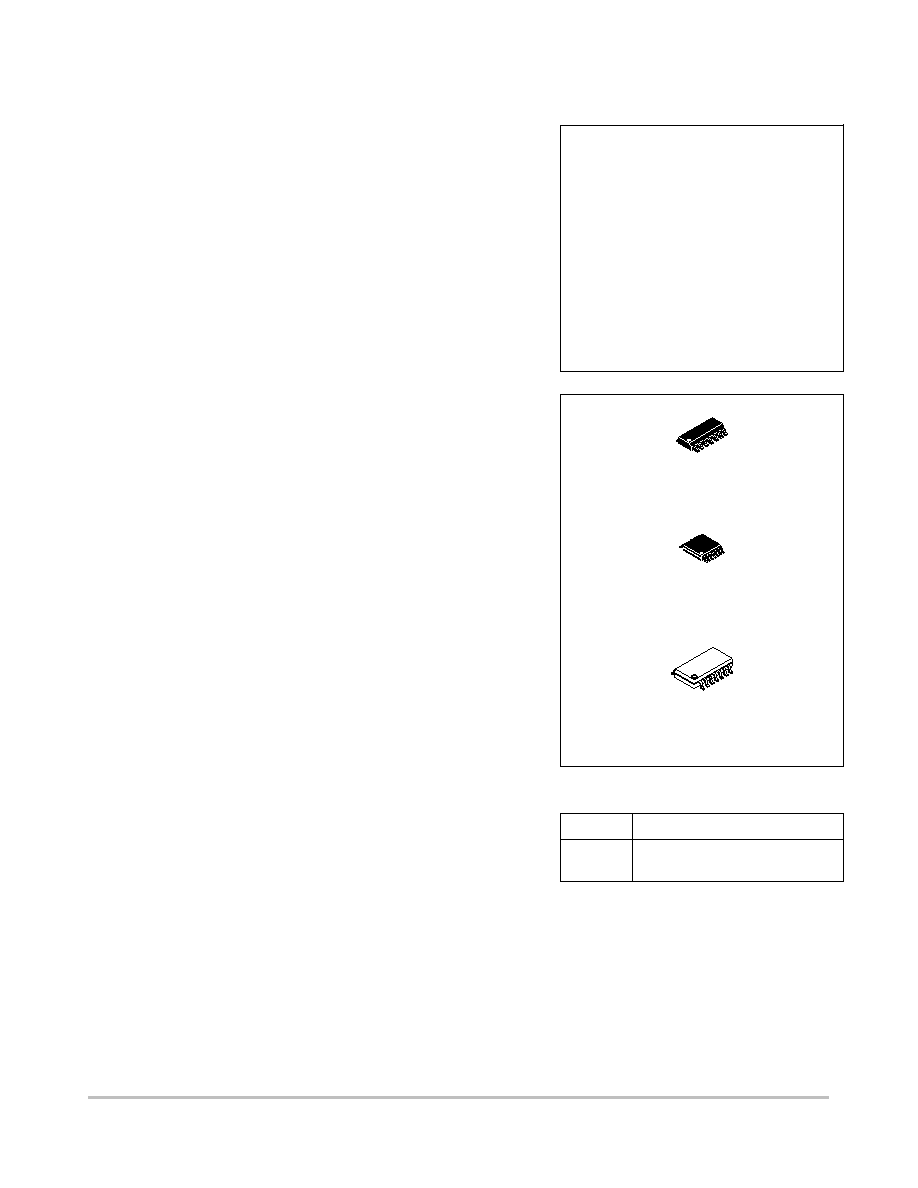
LVX
MC74LVX08
LOW¡VOLTAGE CMOS
D SUFFIX
14¡LEAD SOIC PACKAGE
CASE 751A¡03
DT SUFFIX
14¡LEAD TSSOP PACKAGE
CASE 948G¡01
M SUFFIX
14¡LEAD SOIC EIAJ PACKAGE
CASE 965¡01
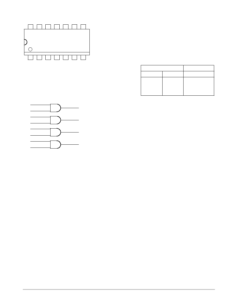
PIN NAMES
Function
Data Inputs
Outputs
Pins
An, Bn
On
⌐
Semiconductor Components Industries, LLC, 2001
February, 2001 ¡ Rev. 1
1
Publication Order Number:
MC74LVX08/D
MC74LVX08
http://onsemi.com
2
Figure 1. 14¡Lead Pinout (Top View)
Figure 2. Figure 1. Logic Diagram
13
14
12
11
10
9
8
2
1
3
4
5
6
7
V
CC
A2
B2
O2
A3
B3
O3
A0
B0
O0
A1
B1
O1
GND
3
O0
1
A0
2
B0
6
O1
4
A1
5
B1
11
O2
13
A2
12
B2
8
O3
10
A3
9
B3
L
L
H
H
L
H
L
H
INPUTS
OUTPUTS
An
Bn
L
L
L
H
On
FUNCTION TABLE
MC74LVX08
http://onsemi.com
3
╬╬╬╬╬╬╬╬╬╬╬╬╬╬╬╬╬╬╬╬╬╬╬╬╬╬╬╬╬╬╬╬╬
╬╬╬╬╬╬╬╬╬╬╬╬╬╬╬╬╬╬╬╬╬╬╬╬╬╬╬╬╬╬╬╬╬
MAXIMUM RATINGS*
╬╬╬╬
╬╬╬╬
Symbol
╬╬╬╬╬╬╬╬╬╬╬╬╬╬╬╬╬╬╬╬╬╬╬
╬╬╬╬╬╬╬╬╬╬╬╬╬╬╬╬╬╬╬╬╬╬╬
Parameter
╬╬╬╬╬╬╬
╬╬╬╬╬╬╬
Value
╬╬
╬╬
Unit
╬╬╬╬
╬╬╬╬
V
CC
╬╬╬╬╬╬╬╬╬╬╬╬╬╬╬╬╬╬╬╬╬╬╬
╬╬╬╬╬╬╬╬╬╬╬╬╬╬╬╬╬╬╬╬╬╬╬
DC Supply Voltage
╬╬╬╬╬╬╬
╬╬╬╬╬╬╬
¡0.5 to +7.0
╬╬
╬╬
V
╬╬╬╬
╬╬╬╬
V
in
╬╬╬╬╬╬╬╬╬╬╬╬╬╬╬╬╬╬╬╬╬╬╬
╬╬╬╬╬╬╬╬╬╬╬╬╬╬╬╬╬╬╬╬╬╬╬
DC Input Voltage
╬╬╬╬╬╬╬
╬╬╬╬╬╬╬
¡0.5 to +7.0
╬╬
╬╬
V
╬╬╬╬
╬╬╬╬
V
out
╬╬╬╬╬╬╬╬╬╬╬╬╬╬╬╬╬╬╬╬╬╬╬
╬╬╬╬╬╬╬╬╬╬╬╬╬╬╬╬╬╬╬╬╬╬╬
DC Output Voltage
╬╬╬╬╬╬╬
╬╬╬╬╬╬╬
¡0.5 to V
CC
+0.5
╬╬
╬╬
V
╬╬╬╬
╬╬╬╬
I
IK
╬╬╬╬╬╬╬╬╬╬╬╬╬╬╬╬╬╬╬╬╬╬╬
╬╬╬╬╬╬╬╬╬╬╬╬╬╬╬╬╬╬╬╬╬╬╬
Input Diode Current
╬╬╬╬╬╬╬
╬╬╬╬╬╬╬
¡20
╬╬
╬╬
mA
╬╬╬╬
╬╬╬╬
I
OK
╬╬╬╬╬╬╬╬╬╬╬╬╬╬╬╬╬╬╬╬╬╬╬
╬╬╬╬╬╬╬╬╬╬╬╬╬╬╬╬╬╬╬╬╬╬╬
Output Diode Current
╬╬╬╬╬╬╬
╬╬╬╬╬╬╬
▒
20
╬╬
╬╬
mA
╬╬╬╬
╬╬╬╬
I
out
╬╬╬╬╬╬╬╬╬╬╬╬╬╬╬╬╬╬╬╬╬╬╬
╬╬╬╬╬╬╬╬╬╬╬╬╬╬╬╬╬╬╬╬╬╬╬
DC Output Current, per Pin
╬╬╬╬╬╬╬
╬╬╬╬╬╬╬
▒
25
╬╬
╬╬
mA
╬╬╬╬
╬╬╬╬
I
CC
╬╬╬╬╬╬╬╬╬╬╬╬╬╬╬╬╬╬╬╬╬╬╬
╬╬╬╬╬╬╬╬╬╬╬╬╬╬╬╬╬╬╬╬╬╬╬
DC Supply Current, V
CC
and GND Pins
╬╬╬╬╬╬╬
╬╬╬╬╬╬╬
▒
50
╬╬
╬╬
mA
╬╬╬╬
╬╬╬╬
P
D
╬╬╬╬╬╬╬╬╬╬╬╬╬╬╬╬╬╬╬╬╬╬╬
╬╬╬╬╬╬╬╬╬╬╬╬╬╬╬╬╬╬╬╬╬╬╬
Power Dissipation
╬╬╬╬╬╬╬
╬╬╬╬╬╬╬
180
╬╬
╬╬
mW
╬╬╬╬
╬╬╬╬
T
stg
╬╬╬╬╬╬╬╬╬╬╬╬╬╬╬╬╬╬╬╬╬╬╬
╬╬╬╬╬╬╬╬╬╬╬╬╬╬╬╬╬╬╬╬╬╬╬
Storage Temperature
╬╬╬╬╬╬╬
╬╬╬╬╬╬╬
¡65 to +150
╬╬
╬╬
_
C
* Absolute maximum continuous ratings are those values beyond which damage to the device may occur. Exposure to these conditions or
conditions beyond those indicated may adversely affect device reliability. Functional operation under absolute¡maximum¡rated conditions
is not implied.
RECOMMENDED OPERATING CONDITIONS
╬╬╬╬
╬╬╬╬
Symbol
╬╬╬╬╬╬╬╬╬╬╬╬╬╬╬╬╬╬╬╬╬╬╬
╬╬╬╬╬╬╬╬╬╬╬╬╬╬╬╬╬╬╬╬╬╬╬
Parameter
╬╬╬╬
╬╬╬╬
Min
╬╬╬╬
╬╬╬╬
Max
╬╬
╬╬
Unit
╬╬╬╬
╬╬╬╬
V
CC
╬╬╬╬╬╬╬╬╬╬╬╬╬╬╬╬╬╬╬╬╬╬╬
╬╬╬╬╬╬╬╬╬╬╬╬╬╬╬╬╬╬╬╬╬╬╬
DC Supply Voltage
╬╬╬╬
╬╬╬╬
2.0
╬╬╬╬
╬╬╬╬
3.6
╬╬
╬╬
V
╬╬╬╬
╬╬╬╬
V
in
╬╬╬╬╬╬╬╬╬╬╬╬╬╬╬╬╬╬╬╬╬╬╬
╬╬╬╬╬╬╬╬╬╬╬╬╬╬╬╬╬╬╬╬╬╬╬
DC Input Voltage
╬╬╬╬
╬╬╬╬
0
╬╬╬╬
╬╬╬╬
5.5
╬╬
╬╬
V
╬╬╬╬
╬╬╬╬
V
out
╬╬╬╬╬╬╬╬╬╬╬╬╬╬╬╬╬╬╬╬╬╬╬
╬╬╬╬╬╬╬╬╬╬╬╬╬╬╬╬╬╬╬╬╬╬╬
DC Output Voltage
╬╬╬╬
╬╬╬╬
0
╬╬╬╬
╬╬╬╬
V
CC
╬╬
╬╬
V
╬╬╬╬
╬╬╬╬
T
A
╬╬╬╬╬╬╬╬╬╬╬╬╬╬╬╬╬╬╬╬╬╬╬
╬╬╬╬╬╬╬╬╬╬╬╬╬╬╬╬╬╬╬╬╬╬╬
Operating Temperature, All Package Types
╬╬╬╬
╬╬╬╬
¡40
╬╬╬╬
╬╬╬╬
+85
╬╬
╬╬
_
C
╬╬╬╬
╬╬╬╬
t/
V
╬╬╬╬╬╬╬╬╬╬╬╬╬╬╬╬╬╬╬╬╬╬╬
╬╬╬╬╬╬╬╬╬╬╬╬╬╬╬╬╬╬╬╬╬╬╬
Input Rise and Fall Time
╬╬╬╬
╬╬╬╬
0
╬╬╬╬
╬╬╬╬
100
╬╬
╬╬
ns/V
╬╬╬╬╬╬╬╬╬╬╬╬╬╬╬╬╬╬╬╬╬╬╬╬╬╬╬╬╬╬╬╬╬
╬╬╬╬╬╬╬╬╬╬╬╬╬╬╬╬╬╬╬╬╬╬╬╬╬╬╬╬╬╬╬╬╬
DC ELECTRICAL CHARACTERISTICS
╬╬╬╬
╬╬╬╬
╬╬╬╬╬╬╬
╬╬╬╬╬╬╬
╬╬╬╬╬╬
╬╬╬╬╬╬
╬╬╬╬
╬╬╬╬
V
CC
╬╬╬╬╬╬╬╬╬
╬╬╬╬╬╬╬╬╬
T
A
= 25
░
C
╬╬╬╬╬╬╬
╬╬╬╬╬╬╬
T
A
= ¡ 40 to 85
░
C
╬╬
╬╬
╬╬╬╬
╬╬╬╬
Symbol
╬╬╬╬╬╬╬
╬╬╬╬╬╬╬
Parameter
╬╬╬╬╬╬
╬╬╬╬╬╬
Test Conditions
╬╬╬╬
╬╬╬╬
V
CC
V
╬╬╬╬
╬╬╬╬
Min
╬╬╬
╬╬╬
Typ
╬╬╬╬
╬╬╬╬
Max
╬╬╬╬
╬╬╬╬
Min
╬╬╬╬
╬╬╬╬
Max
╬╬
╬╬
Unit
╬╬╬╬
╬
╬╬
╬
╬
╬╬
╬
╬╬╬╬
V
IH
╬╬╬╬╬╬╬
╬
╬╬╬╬╬
╬
╬
╬╬╬╬╬
╬
╬╬╬╬╬╬╬
High¡Level Input
Voltage
╬╬╬╬╬╬
╬
╬╬╬╬
╬
╬
╬╬╬╬
╬
╬╬╬╬╬╬
╬╬╬╬
╬
╬╬
╬
╬
╬╬
╬
╬╬╬╬
2.0
3.0
3.6
╬╬╬╬
╬
╬╬
╬
╬
╬╬
╬
╬╬╬╬
1.5
2.0
2.4
╬╬╬
╬
╬
╬
╬
╬
╬
╬╬╬
╬╬╬╬
╬
╬╬
╬
╬
╬╬
╬
╬╬╬╬
╬╬╬╬
╬
╬╬
╬
╬
╬╬
╬
╬╬╬╬
1.5
2.0
2.4
╬╬╬╬
╬
╬╬
╬
╬
╬╬
╬
╬╬╬╬
╬╬
╬╬
╬╬
╬╬
V
╬╬╬╬
╬
╬╬
╬
╬╬╬╬
V
IL
╬╬╬╬╬╬╬
╬
╬╬╬╬╬
╬
╬╬╬╬╬╬╬
Low¡Level Input Voltage
╬╬╬╬╬╬
╬
╬╬╬╬
╬
╬╬╬╬╬╬
╬╬╬╬
╬
╬╬
╬
╬╬╬╬
2.0
3.0
3.6
╬╬╬╬
╬
╬╬
╬
╬╬╬╬
╬╬╬
╬
╬
╬
╬╬╬
╬╬╬╬
╬
╬╬
╬
╬╬╬╬
0.5
0.8
0.8
╬╬╬╬
╬
╬╬
╬
╬╬╬╬
╬╬╬╬
╬
╬╬
╬
╬╬╬╬
0.5
0.8
0.8
╬╬
╬╬
╬╬
V
╬╬╬╬
╬
╬╬
╬
╬╬╬╬
V
OH
╬╬╬╬╬╬╬
╬
╬╬╬╬╬
╬
╬╬╬╬╬╬╬
High¡Level Output
Voltage
(V
in
= V
IH
or V
IL
)
╬╬╬╬╬╬
╬
╬╬╬╬
╬
╬╬╬╬╬╬
I
OH
= ¡50
╡
A
I
OH
= ¡50
╡
A
I
OH
= ¡4mA
╬╬╬╬
╬
╬╬
╬
╬╬╬╬
2.0
3.0
3.0
╬╬╬╬
╬
╬╬
╬
╬╬╬╬
1.9
2.9
2.58
╬╬╬
╬
╬
╬
╬╬╬
2.0
3.0
╬╬╬╬
╬
╬╬
╬
╬╬╬╬
╬╬╬╬
╬
╬╬
╬
╬╬╬╬
1.9
2.9
2.48
╬╬╬╬
╬
╬╬
╬
╬╬╬╬
╬╬
╬╬
╬╬
V
╬╬╬╬
╬
╬╬
╬
╬
╬╬
╬
╬╬╬╬
V
OL
╬╬╬╬╬╬╬
╬
╬╬╬╬╬
╬
╬
╬╬╬╬╬
╬
╬╬╬╬╬╬╬
Low¡Level Output
Voltage
(V
in
= V
IH
or V
IL
)
╬╬╬╬╬╬
╬
╬╬╬╬
╬
╬
╬╬╬╬
╬
╬╬╬╬╬╬
I
OL
= 50
╡
A
I
OL
= 50
╡
A
I
OL
= 4mA
╬╬╬╬
╬
╬╬
╬
╬
╬╬
╬
╬╬╬╬
2.0
3.0
3.0
╬╬╬╬
╬
╬╬
╬
╬
╬╬
╬
╬╬╬╬
╬╬╬
╬
╬
╬
╬
╬
╬
╬╬╬
0.0
0.0
╬╬╬╬
╬
╬╬
╬
╬
╬╬
╬
╬╬╬╬
0.1
0.1
0.36
╬╬╬╬
╬
╬╬
╬
╬
╬╬
╬
╬╬╬╬
╬╬╬╬
╬
╬╬
╬
╬
╬╬
╬
╬╬╬╬
0.1
0.1
0.44
╬╬
╬╬
╬╬
╬╬
V
╬╬╬╬
╬╬╬╬
I
in
╬╬╬╬╬╬╬
╬╬╬╬╬╬╬
Input Leakage Current
╬╬╬╬╬╬
╬╬╬╬╬╬
V
in
= 5.5V or GND
╬╬╬╬
╬╬╬╬
3.6
╬╬╬╬
╬╬╬╬
╬╬╬
╬╬╬
╬╬╬╬
╬╬╬╬
▒
0.1
╬╬╬╬
╬╬╬╬
╬╬╬╬
╬╬╬╬
▒
1.0
╬╬
╬╬
╡
A
╬╬╬╬
╬╬╬╬
I
CC
╬╬╬╬╬╬╬
╬╬╬╬╬╬╬
Quiescent Supply
Current
╬╬╬╬╬╬
╬╬╬╬╬╬
V
in
= V
CC
or GND
╬╬╬╬
╬╬╬╬
3.6
╬╬╬╬
╬╬╬╬
╬╬╬
╬╬╬
╬╬╬╬
╬╬╬╬
2.0
╬╬╬╬
╬╬╬╬
╬╬╬╬
╬╬╬╬
20.0
╬╬
╬╬
╡
A
MC74LVX08
http://onsemi.com
4
╬╬╬╬╬╬╬╬╬╬╬╬╬╬╬╬╬╬╬╬╬╬╬╬╬╬╬╬╬╬╬╬╬
╬╬╬╬╬╬╬╬╬╬╬╬╬╬╬╬╬╬╬╬╬╬╬╬╬╬╬╬╬╬╬╬╬
AC ELECTRICAL CHARACTERISTICS
(Input t
r
= t
f
= 3.0ns)
╬╬╬╬
╬╬╬╬
╬╬╬╬╬╬╬╬╬
╬╬╬╬╬╬╬╬╬
╬╬╬╬╬╬╬╬
╬╬╬╬╬╬╬╬
╬╬╬╬╬╬╬╬╬
╬╬╬╬╬╬╬╬╬
T
A
= 25
░
C
╬╬╬╬╬╬
╬╬╬╬╬╬
T
A
= ¡ 40 to 85
░
C
╬╬
╬╬
╬╬╬╬
╬╬╬╬
Symbol
╬╬╬╬╬╬╬╬╬
╬╬╬╬╬╬╬╬╬
Parameter
╬╬╬╬╬╬╬╬
╬╬╬╬╬╬╬╬
Test Conditions
╬╬╬╬
╬╬╬╬
Min
╬╬╬
╬╬╬
Typ
╬╬╬╬
╬╬╬╬
Max
╬╬╬
╬╬╬
Min
╬╬╬╬
╬╬╬╬
Max
╬╬
╬╬
Unit
╬╬╬╬
╬
╬╬
╬
╬╬╬╬
t
PLH
,
t
PHL
╬╬╬╬╬╬╬╬╬
╬
╬╬╬╬╬╬╬
╬
╬╬╬╬╬╬╬╬╬
Propagation Delay, Input to
Output
╬╬╬╬╬╬╬╬
╬
╬╬╬╬╬╬
╬
╬╬╬╬╬╬╬╬
V
CC
= 2.7V
C
L
= 15pF
C
L
= 50pF
╬╬╬╬
╬
╬╬
╬
╬╬╬╬
╬╬╬
╬
╬
╬
╬╬╬
6.3
8.8
╬╬╬╬
╬
╬╬
╬
╬╬╬╬
11.4
14.9
╬╬╬
╬
╬
╬
╬╬╬
1.0
1.0
╬╬╬╬
╬
╬╬
╬
╬╬╬╬
13.5
17.0
╬╬
╬╬
╬╬
ns
╬╬╬╬
╬╬╬╬
╬╬╬╬╬╬╬╬╬
╬╬╬╬╬╬╬╬╬
╬╬╬╬╬╬╬╬
╬╬╬╬╬╬╬╬
V
CC
= 3.3
▒
0.3V
C
L
= 15pF
C
L
= 50pF
╬╬╬╬
╬╬╬╬
╬╬╬
╬╬╬
4.8
7.3
╬╬╬╬
╬╬╬╬
7.1
10.6
╬╬╬
╬╬╬
1.0
1.0
╬╬╬╬
╬╬╬╬
8.5
12.0
╬╬
╬╬
╬╬╬╬
╬
╬╬
╬
╬╬╬╬
t
OSHL
t
OSLH
╬╬╬╬╬╬╬╬╬
╬
╬╬╬╬╬╬╬
╬
╬╬╬╬╬╬╬╬╬
Output¡to¡Output Skew
(Note NO TAG)
╬╬╬╬╬╬╬╬
╬
╬╬╬╬╬╬
╬
╬╬╬╬╬╬╬╬
V
CC
= 2.7V
C
L
= 50pF
V
CC
= 3.3
▒
0.3V
C
L
= 50pF
╬╬╬╬
╬
╬╬
╬
╬╬╬╬
╬╬╬
╬
╬
╬
╬╬╬
╬╬╬╬
╬
╬╬
╬
╬╬╬╬
1.5
1.5
╬╬╬
╬
╬
╬
╬╬╬
╬╬╬╬
╬
╬╬
╬
╬╬╬╬
1.5
1.5
╬╬
╬╬
╬╬
ns
1. Skew is defined as the absolute value of the difference between the actual propagation delay for any two separate outputs of the same device.
The specification applies to any outputs switching in the same direction, either HIGH¡to¡LOW (t
OSHL
) or LOW¡to¡HIGH (t
OSLH
); parameter
guaranteed by design.
╬╬╬╬╬╬╬╬╬╬╬╬╬╬╬╬╬╬╬╬╬╬╬╬╬╬╬╬╬╬╬╬╬
CAPACITIVE CHARACTERISTICS
╬╬╬╬
╬╬╬╬
╬╬╬╬╬╬╬╬╬╬╬╬╬╬╬╬
╬╬╬╬╬╬╬╬╬╬╬╬╬╬╬╬
╬╬╬╬╬╬╬╬╬
╬╬╬╬╬╬╬╬╬
T
A
= 25
░
C
╬╬╬╬╬╬
╬╬╬╬╬╬
T
A
= ¡ 40 to 85
░
C
╬╬
╬╬
╬╬╬╬
╬╬╬╬
Symbol
╬╬╬╬╬╬╬╬╬╬╬╬╬╬╬╬
╬╬╬╬╬╬╬╬╬╬╬╬╬╬╬╬
Parameter
╬╬╬╬
╬╬╬╬
Min
╬╬╬
╬╬╬
Typ
╬╬╬╬
╬╬╬╬
Max
╬╬╬
╬╬╬
Min
╬╬╬╬
╬╬╬╬
Max
╬╬
╬╬
Unit
╬╬╬╬
╬╬╬╬
C
in
╬╬╬╬╬╬╬╬╬╬╬╬╬╬╬╬
╬╬╬╬╬╬╬╬╬╬╬╬╬╬╬╬
Input Capacitance
╬╬╬╬
╬╬╬╬
╬╬╬
╬╬╬
4
╬╬╬╬
╬╬╬╬
10
╬╬╬
╬╬╬
╬╬╬╬
╬╬╬╬
10
╬╬
╬╬
pF
╬╬╬╬
╬╬╬╬
C
PD
╬╬╬╬╬╬╬╬╬╬╬╬╬╬╬╬
╬╬╬╬╬╬╬╬╬╬╬╬╬╬╬╬
Power Dissipation Capacitance (Note NO TAG)
╬╬╬╬
╬╬╬╬
╬╬╬
╬╬╬
18
╬╬╬╬
╬╬╬╬
╬╬╬
╬╬╬
╬╬╬╬
╬╬╬╬
╬╬
╬╬
pF
2. C
PD
is defined as the value of the internal equivalent capacitance which is calculated from the operating current consumption without load.
Average operating current can be obtained by the equation: I
CC(OPR
)
= C
PD
V
CC
f
in
+ I
CC
/4 (per gate). C
PD
is used to determine the no¡load
dynamic power consumption; P
D
= C
PD
V
CC
2
f
in
+ I
CC
V
CC
.
NOISE CHARACTERISTICS
(Input t
r
= t
f
= 3.0ns, C
L
= 50pF, V
CC
= 3.3V, Measured in SOIC Package)
T
A
= 25
░
C
Symbol
Characteristic
Typ
Max
Unit
V
OLP
Quiet Output Maximum Dynamic V
OL
0.3
0.5
V
V
OLV
Quiet Output Minimum Dynamic V
OL
¡0.3
¡0.5
V
V
IHD
Minimum High Level Dynamic Input Voltage
2.0
V
V
ILD
Maximum Low Level Dynamic Input Voltage
0.8
V
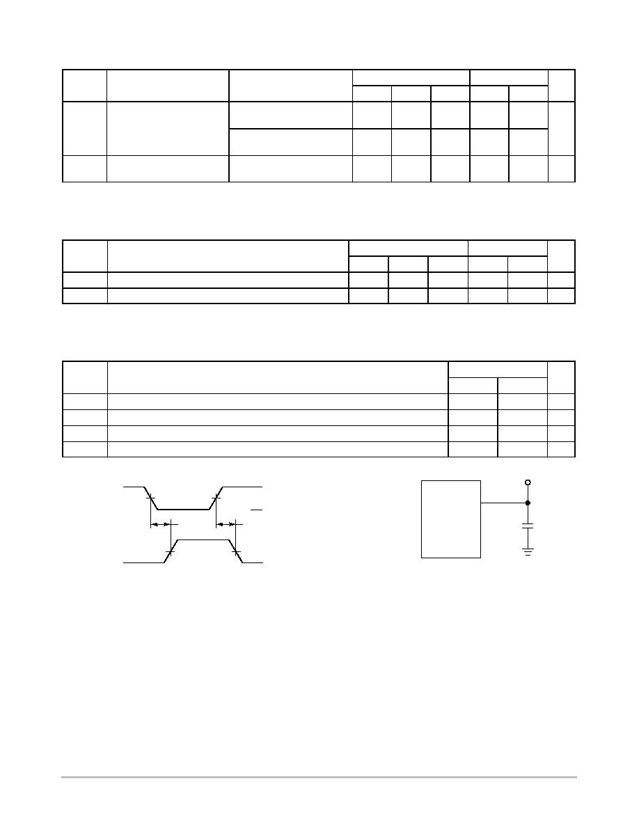
Figure 3. Switching Waveforms
V
CC
GND
50%
50% V
CC
A or B
O
t
PHL
t
PLH
*Includes all probe and jig capacitance
Figure 4. Test Circuit
C
L
*
TEST POINT
DEVICE
UNDER
TEST
OUTPUT
MC74LVX08
http://onsemi.com
5
OUTLINE DIMENSIONS
D SUFFIX
PLASTIC SOIC PACKAGE
CASE 751A¡03
ISSUE F
MIN
MIN
MAX
MAX
MILLIMETERS
INCHES
DIM
A
B
C
D
F
G
J
K
M
P
R
8.55
3.80
1.35
0.35
0.40
0.19
0.10
0
░
5.80
0.25
8.75
4.00
1.75
0.49
1.25
0.25
0.25
7
░
6.20
0.50
0.337
0.150
0.054
0.014
0.016
0.008
0.004
0
░
0.228
0.010
0.344
0.157
0.068
0.019
0.049
0.009
0.009
7
░
0.244
0.019
1.27 BSC
0.050 BSC
NOTES:
1. DIMENSIONING AND TOLERANCING PER ANSI
Y14.5M, 1982.
2. CONTROLLING DIMENSION: MILLIMETER.
3. DIMENSIONS A AND B DO NOT INCLUDE
MOLD PROTRUSION.
4. MAXIMUM MOLD PROTRUSION 0.15 (0.006)
PER SIDE.
5. DIMENSION D DOES NOT INCLUDE DAMBAR
PROTRUSION. ALLOWABLE DAMBAR
PROTRUSION SHALL BE 0.127 (0.005) TOTAL
IN EXCESS OF THE D DIMENSION AT
MAXIMUM MATERIAL CONDITION.
¡A
¡
¡B
¡
P
7 PL
G
C
K
SEATING
PLANE
D
14 PL
M
J
R
X 45
░
1
7
8
14
0.25 (0.010)
T B
A
M
S
S
B
0.25 (0.010)
M
M
F
MC74LVX08
http://onsemi.com
6
OUTLINE DIMENSIONS
M SUFFIX
PLASTIC SOIC EIAJ PACKAGE
CASE 965¡01
ISSUE O
Z
D
H
E
E
1
14
8
7
b
A
1
A
e
L
DIM
MIN
MAX
MIN
MAX
INCHES
2.05
0.081
MILLIMETERS
0.05
0.20
0.002
0.008
0.35
0.50
0.014
0.020
0.18
0.27
0.007
0.011
9.90
10.50
0.390
0.413
5.10
5.45
0.201
0.215
1.27 BSC
0.050 BSC
7.40
8.20
0.291
0.323
0.50
0.85
0.020
0.033
1.10
1.50
0.043
0.059
0
0.70
0.90
0.028
0.035
1.42
0.056
A
1
A
b
c
D
E
e
L
M
Z
H
E
Q
1
L
E
_
10
_
0
_
10
_
L
E
Q
1
c
M
_
VIEW P
DETAIL P
NOTES:
1. DIMENSIONING AND TOLERANCING PER ANSI
Y14.5M, 1982.
2. CONTROLLING DIMENSION: MILLIMETER.
3. DIMENSIONS D AND E DO NOT INCLUDE MOLD
FLASH OR PROTRUSIONS AND ARE MEASURED
AT THE PARTING LINE. MOLD FLASH OR
PROTRUSIONS SHALL NOT EXCEED 0.15 (0.006)
PER SIDE.
4. TERMINAL NUMBERS ARE SHOWN FOR
REFERENCE ONLY.
5. THE LEAD WIDTH DIMENSION (b) DOES NOT
INCLUDE DAMBAR PROTRUSION. ALLOWABLE
DAMBAR PROTRUSION SHALL BE 0.08 (0.003)
TOTAL IN EXCESS OF THE LEAD WIDTH
DIMENSION AT MAXIMUM MATERIAL CONDITION.
DAMBAR CANNOT BE LOCATED ON THE LOWER
RADIUS OR THE FOOT. MINIMUM SPACE
BETWEEN PROTRUSIONS AND ADJACENT LEAD
TO BE 0.46 ( 0.018).
0.13 (0.005)
M
0.10 (0.004)
MC74LVX08
http://onsemi.com
7
OUTLINE DIMENSIONS
DT SUFFIX
PLASTIC TSSOP PACKAGE
CASE 948G¡01
ISSUE O
DIM
MIN
MAX
MIN
MAX
INCHES
MILLIMETERS
A
4.90
5.10
0.193
0.200
B
4.30
4.50
0.169
0.177
C
---
1.20
---
0.047
D
0.05
0.15
0.002
0.006
F
0.50
0.75
0.020
0.030
G
0.65 BSC
0.026 BSC
H
0.50
0.60
0.020
0.024
J
0.09
0.20
0.004
0.008
J1
0.09
0.16
0.004
0.006
K
0.19
0.30
0.007
0.012
K1
0.19
0.25
0.007
0.010
L
6.40 BSC
0.252 BSC
M
0
8
0
8
NOTES:
1. DIMENSIONING AND TOLERANCING PER ANSI
Y14.5M, 1982.
2. CONTROLLING DIMENSION: MILLIMETER.
3. DIMENSION A DOES NOT INCLUDE MOLD
FLASH, PROTRUSIONS OR GATE BURRS.
MOLD FLASH OR GATE BURRS SHALL NOT
EXCEED 0.15 (0.006) PER SIDE.
4. DIMENSION B DOES NOT INCLUDE INTERLEAD
FLASH OR PROTRUSION. INTERLEAD FLASH
OR PROTRUSION SHALL NOT EXCEED
0.25 (0.010) PER SIDE.
5. DIMENSION K DOES NOT INCLUDE DAMBAR
PROTRUSION. ALLOWABLE DAMBAR
PROTRUSION SHALL BE 0.08 (0.003) TOTAL IN
EXCESS OF THE K DIMENSION AT MAXIMUM
MATERIAL CONDITION.
6. TERMINAL NUMBERS ARE SHOWN FOR
REFERENCE ONLY.
7. DIMENSION A AND B ARE TO BE DETERMINED
AT DATUM PLANE -W-.
_
_
_
_
S
U
0.15 (0.006) T
2X
L/2
S
U
M
0.10 (0.004)
V
S
T
L
¡U¡
SEATING
PLANE
0.10 (0.004)
¡T¡
╟╟╟
╟╟╟
SECTION N¡N
DETAIL E
J J1
K
K1
╔╔
╔╔
DETAIL E
F
M
¡W¡
0.25 (0.010)
8
14
7
1
PIN 1
IDENT.
H
G
A
D
C
B
S
U
0.15 (0.006) T
¡V¡
14X REF
K
N
N

MC74LVX08
http://onsemi.com
8
ON Semiconductor and are trademarks of Semiconductor Components Industries, LLC (SCILLC). SCILLC reserves the right to make changes
without further notice to any products herein. SCILLC makes no warranty, representation or guarantee regarding the suitability of its products for any particular
purpose, nor does SCILLC assume any liability arising out of the application or use of any product or circuit, and specifically disclaims any and all liability,
including without limitation special, consequential or incidental damages. "Typical" parameters which may be provided in SCILLC data sheets and/or
specifications can and do vary in different applications and actual performance may vary over time. All operating parameters, including "Typicals" must be
validated for each customer application by customer's technical experts. SCILLC does not convey any license under its patent rights nor the rights of others.
SCILLC products are not designed, intended, or authorized for use as components in systems intended for surgical implant into the body, or other applications
intended to support or sustain life, or for any other application in which the failure of the SCILLC product could create a situation where personal injury or
death may occur. Should Buyer purchase or use SCILLC products for any such unintended or unauthorized application, Buyer shall indemnify and hold
SCILLC and its officers, employees, subsidiaries, affiliates, and distributors harmless against all claims, costs, damages, and expenses, and reasonable
attorney fees arising out of, directly or indirectly, any claim of personal injury or death associated with such unintended or unauthorized use, even if such claim
alleges that SCILLC was negligent regarding the design or manufacture of the part. SCILLC is an Equal Opportunity/Affirmative Action Employer.
PUBLICATION ORDERING INFORMATION
CENTRAL/SOUTH AMERICA:
Spanish Phone: 303¡308¡7143 (Mon¡Fri 8:00am to 5:00pm MST)
Email: ONlit¡spanish@hibbertco.com
Toll¡Free from Mexico: Dial 01¡800¡288¡2872 for Access ¡
then Dial 866¡297¡9322
ASIA/PACIFIC: LDC for ON Semiconductor ¡ Asia Support
Phone: 303¡675¡2121 (Tue¡Fri 9:00am to 1:00pm, Hong Kong Time)
Toll Free from Hong Kong & Singapore:
001¡800¡4422¡3781
Email: ONlit¡asia@hibbertco.com
JAPAN: ON Semiconductor, Japan Customer Focus Center
4¡32¡1 Nishi¡Gotanda, Shinagawa¡ku, Tokyo, Japan 141¡0031
Phone: 81¡3¡5740¡2700
Email: r14525@onsemi.com
ON Semiconductor Website: http://onsemi.com
For additional information, please contact your local
Sales Representative.
MC74LVX08/D
NORTH AMERICA Literature Fulfillment:
Literature Distribution Center for ON Semiconductor
P.O. Box 5163, Denver, Colorado 80217 USA
Phone: 303¡675¡2175 or 800¡344¡3860 Toll Free USA/Canada
Fax: 303¡675¡2176 or 800¡344¡3867 Toll Free USA/Canada
Email: ONlit@hibbertco.com
Fax Response Line: 303¡675¡2167 or 800¡344¡3810 Toll Free USA/Canada
N. American Technical Support: 800¡282¡9855 Toll Free USA/Canada
EUROPE: LDC for ON Semiconductor ¡ European Support
German Phone: (+1) 303¡308¡7140 (Mon¡Fri 2:30pm to 7:00pm CET)
Email: ONlit¡german@hibbertco.com
French Phone: (+1) 303¡308¡7141 (Mon¡Fri 2:00pm to 7:00pm CET)
Email: ONlit¡french@hibbertco.com
English Phone: (+1) 303¡308¡7142 (Mon¡Fri 12:00pm to 5:00pm GMT)
Email: ONlit@hibbertco.com
EUROPEAN TOLL¡FREE ACCESS*: 00¡800¡4422¡3781
*Available from Germany, France, Italy, UK, Ireland