
MC74VHC138
3-to-8 Line Decoder
The MC74VHC138 is an advanced high speed CMOS 3≠to≠8
decoder fabricated with silicon gate CMOS technology. It achieves
high speed operation similar to equivalent Bipolar Schottky TTL
while maintaining CMOS low power dissipation.
When the device is enabled, three Binary Select inputs (A0 ≠ A2)
determine which one of the outputs (Y0 ≠ Y7) will go Low. When
enable input E3 is held Low or either E2 or E1 is held High, decoding
function is inhibited and all outputs go high. E3, E2, and E1 inputs are
provided to ease cascade connection and for use as an address decoder
for memory systems.
The internal circuit is composed of three stages, including a buffer
output which provides high noise immunity and stable output. The
inputs tolerate voltages up to 7V, allowing the interface of 5V systems
to 3V systems.
∑
High Speed: t
PD
= 5.7ns (Typ) at V
CC
= 5V
∑
Low Power Dissipation: I
CC
= 4
µ
A (Max) at T
A
= 25
∞
C
∑
High Noise Immunity: V
NIH
= V
NIL
= 28% V
CC
∑
Power Down Protection Provided on Inputs
∑
Balanced Propagation Delays
∑
Designed for 2V to 5.5V Operating Range
∑
Low Noise: V
OLP
= 0.8 V (Max)
∑
Pin and Function Compatible with Other Standard Logic Families
∑
Latchup Performance Exceeds 300mA
∑
ESD Performance: HBM > 2000V; Machine Model > 200V
∑
Chip Complexity: 122 FETs or 30.5 Equivalent Gates
©
Semiconductor Components Industries, LLC, 2001
March, 2001 ≠ Rev. 3
1
Publication Order Number:
MC74VHC138/D
Device
Package
Shipping
ORDERING INFORMATION
MC74VHC138D
SOIC≠16
48 Units/Rail
MC74VHC138DR2
SOIC≠16
http://onsemi.com
2500 Units/Reel
SOIC≠16
D SUFFIX
CASE 751B
TSSOP≠16
DT SUFFIX
CASE 948F
SOIC EIAJ≠16
M SUFFIX
CASE 966
MARKING DIAGRAMS
1
8
9
16
1
8
16
9
1
16
9
8
VHC138
AWLYYWW
A
= Assembly Location
WL = Wafer Lot
YY = Year
WW = Work Week
VHC
138
AWLYWW
VHC138
ALYW
MC74VHC138DT
TSSOP≠16
96 Units/Rail
MC74VHC138DTR2 TSSOP≠16
2500 Units/Reel
MC74VHC138M
SOIC
EIAJ≠16
48 Units/Rail
MC74VHC138MEL
SOIC
EIAJ≠16
2000 Units/Reel
A = Assembly Location
L
= Wafer Lot
Y = Year
W = Work Week
A
= Assembly Location
WL = Wafer Lot
Y
= Year
WW = Work Week
MC74VHC138
http://onsemi.com
2
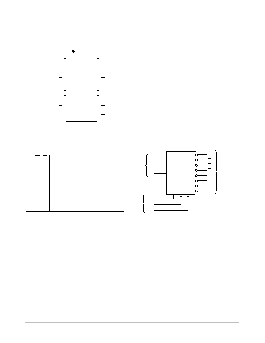
PIN ASSIGNMENT
13
14
15
16
9
10
11
12
5
4
3
2
1
8
7
6
A0
E1
A2
A1
Y7
E3
E2
GND
Y3
Y2
Y1
Y0
V
CC
Y5
Y4
Y6
7
Y6
Y5
Y4
Y3
Y2
Y1
Y0
Y7
9
10
11
12
13
14
15
3
2
1
E3
E2
A0
A1
A2
ACTIVE-LOW
OUTPUTS
SELECT
INPUTS
E1
ENABLE
INPUTS
4
5
6
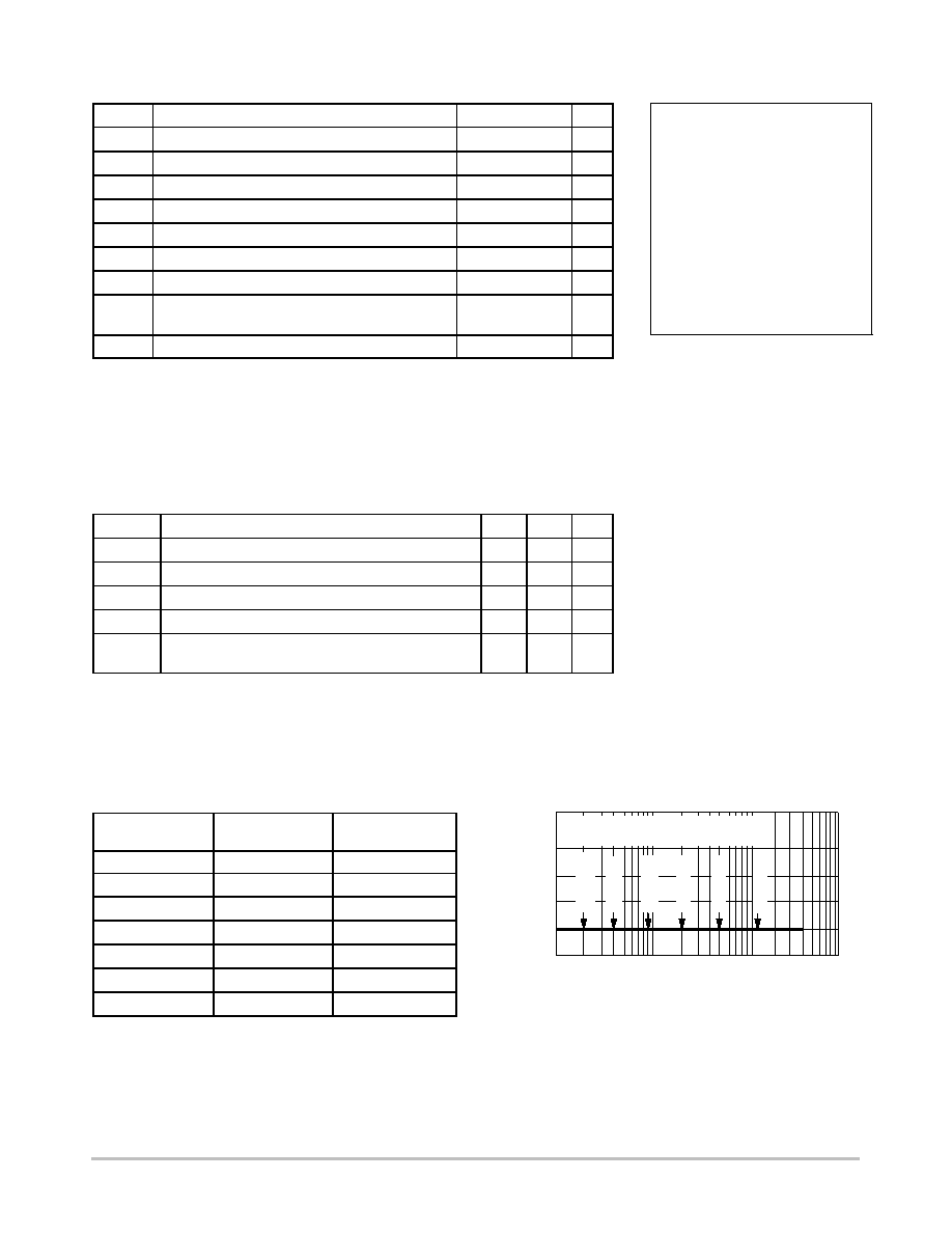
Inputs
Outputs
E3
E2
E1
A2 A1 A0 Y0 Y1 Y2 Y3 Y4 Y5 Y6 Y7
X
X
H
X
X
X
H
H
H
H
H
H
H
H
X
H
X
X
X
X
H
H
H
H
H
H
H
H
L
X
X
X
X
X
H
H
H
H
H
H
H
H
H
L
L
L
L
L
L
H
H
H
H
H
H
H
H
L
L
L
L
H
H
L
H
H
H
H
H
H
H
L
L
L
H
L
H
H
L
H
H
H
H
H
H
L
L
L
H
H
H
H
H
L
H
H
H
H
H
L
L
H
L
L
H
H
H
H
L
H
H
H
H
L
L
H
L
H
H
H
H
H
H
L
H
H
H
L
L
H
H
L
H
H
H
H
H
H
L
H
H
L
L
H
H
H
H
H
H
H
H
H
H
L
FUNCTION TABLE
H = high level (steady state); L = low level (steady state);
X = don't care
LOGIC DIAGRAM

MC74VHC138
http://onsemi.com
3
A0
A1
A2
E2
E1
E3
1
2
3
4
5
6
15
14
13
12
11
10
9
7
Y1
Y2
Y3
Y4
Y5
Y6
Y7
Y0
EXPANDED LOGIC DIAGRAM
15
IEC LOGIC DIAGRAM
Y0
Y1
Y2
Y3
Y4
Y5
Y6
Y7
14
13
12
11
10
9
7
4
5
6
3
2
1
A0
A1
A2
E3
E2
E1
2
1
4
BIN/OCT
1
0
2
4
3
5
6
7
EN
&
15 Y0
Y1
Y2
Y3
Y4
Y5
Y6
Y7
14
13
12
11
10
9
7
4
5
6
3
2
1
A0
A1
A2
E3
E2
E1
0
2
DMUX
1
0
2
4
3
5
6
7
&
G 0
7
MC74VHC138
http://onsemi.com
4
ŒŒŒŒŒŒŒŒŒŒŒŒŒŒŒŒŒŒŒŒŒŒŒ
ŒŒŒŒŒŒŒŒŒŒŒŒŒŒŒŒŒŒŒŒŒŒŒ
MAXIMUM RATINGS*
ŒŒŒŒ
ŒŒŒŒ
Symbol
ŒŒŒŒŒŒŒŒŒŒŒŒŒŒ
ŒŒŒŒŒŒŒŒŒŒŒŒŒŒ
Parameter
ŒŒŒŒŒ
ŒŒŒŒŒ
Value
ŒŒŒ
ŒŒŒ
Unit
ŒŒŒŒ
ŒŒŒŒ
V
CC
ŒŒŒŒŒŒŒŒŒŒŒŒŒŒ
ŒŒŒŒŒŒŒŒŒŒŒŒŒŒ
DC Supply Voltage
ŒŒŒŒŒ
ŒŒŒŒŒ
≠ 0.5 to + 7.0
ŒŒŒ
ŒŒŒ
V
ŒŒŒŒ
ŒŒŒŒ
V
in
ŒŒŒŒŒŒŒŒŒŒŒŒŒŒ
ŒŒŒŒŒŒŒŒŒŒŒŒŒŒ
DC Input Voltage
ŒŒŒŒŒ
ŒŒŒŒŒ
≠ 0.5 to + 7.0
ŒŒŒ
ŒŒŒ
V
ŒŒŒŒ
ŒŒŒŒ
V
out
ŒŒŒŒŒŒŒŒŒŒŒŒŒŒ
ŒŒŒŒŒŒŒŒŒŒŒŒŒŒ
DC Output Voltage
ŒŒŒŒŒ
ŒŒŒŒŒ
≠ 0.5 to V
CC
+ 0.5
ŒŒŒ
ŒŒŒ
V
ŒŒŒŒ
ŒŒŒŒ
I
IK
ŒŒŒŒŒŒŒŒŒŒŒŒŒŒ
ŒŒŒŒŒŒŒŒŒŒŒŒŒŒ
Input Diode Current
ŒŒŒŒŒ
ŒŒŒŒŒ
≠ 20
ŒŒŒ
ŒŒŒ
mA
ŒŒŒŒ
ŒŒŒŒ
I
OK
ŒŒŒŒŒŒŒŒŒŒŒŒŒŒ
ŒŒŒŒŒŒŒŒŒŒŒŒŒŒ
Output Diode Current
ŒŒŒŒŒ
ŒŒŒŒŒ
±
20
ŒŒŒ
ŒŒŒ
mA
ŒŒŒŒ
ŒŒŒŒ
I
out
ŒŒŒŒŒŒŒŒŒŒŒŒŒŒ
ŒŒŒŒŒŒŒŒŒŒŒŒŒŒ
DC Output Current, per Pin
ŒŒŒŒŒ
ŒŒŒŒŒ
±
25
ŒŒŒ
ŒŒŒ
mA
ŒŒŒŒ
ŒŒŒŒ
I
CC
ŒŒŒŒŒŒŒŒŒŒŒŒŒŒ
ŒŒŒŒŒŒŒŒŒŒŒŒŒŒ
DC Supply Current, V
CC
and GND Pins
ŒŒŒŒŒ
ŒŒŒŒŒ
±
75
ŒŒŒ
ŒŒŒ
mA
ŒŒŒŒ
Œ
ŒŒ
Œ
ŒŒŒŒ
P
D
ŒŒŒŒŒŒŒŒŒŒŒŒŒŒ
Œ
ŒŒŒŒŒŒŒŒŒŒŒŒ
Œ
ŒŒŒŒŒŒŒŒŒŒŒŒŒŒ
Power Dissipation in Still Air,
SOIC Packages
TSSOP Package
ŒŒŒŒŒ
Œ
ŒŒŒ
Œ
ŒŒŒŒŒ
500
450
ŒŒŒ
Œ
Œ
Œ
ŒŒŒ
mW
ŒŒŒŒ
ŒŒŒŒ
T
stg
ŒŒŒŒŒŒŒŒŒŒŒŒŒŒ
ŒŒŒŒŒŒŒŒŒŒŒŒŒŒ
Storage Temperature
ŒŒŒŒŒ
ŒŒŒŒŒ
≠ 65 to + 150
ŒŒŒ
ŒŒŒ
_
C
* Absolute maximum continuous ratings are those values beyond which damage to the device
may occur. Exposure to these conditions or conditions beyond those indicated may
adversely affect device reliability. Functional operation under absolute≠maximum≠rated
conditions is not implied.
Derating -- SOIC Packages: ≠ 7 mW/
_
C from 65
_
to 125
_
C
TSSOP Package: ≠ 6.1 mW/
_
C from 65
_
to 125
_
C
RECOMMENDED OPERATING CONDITIONS
ŒŒŒŒ
ŒŒŒŒ
Symbol
ŒŒŒŒŒŒŒŒŒŒŒŒŒŒŒ
ŒŒŒŒŒŒŒŒŒŒŒŒŒŒŒ
Parameter
ŒŒŒ
ŒŒŒ
Min
ŒŒ
ŒŒ
Max
ŒŒŒ
ŒŒŒ
Unit
ŒŒŒŒ
ŒŒŒŒ
V
CC
ŒŒŒŒŒŒŒŒŒŒŒŒŒŒŒ
ŒŒŒŒŒŒŒŒŒŒŒŒŒŒŒ
DC Supply Voltage
ŒŒŒ
ŒŒŒ
2.0
ŒŒ
ŒŒ
5.5
ŒŒŒ
ŒŒŒ
V
ŒŒŒŒ
ŒŒŒŒ
V
in
ŒŒŒŒŒŒŒŒŒŒŒŒŒŒŒ
ŒŒŒŒŒŒŒŒŒŒŒŒŒŒŒ
DC Input Voltage
ŒŒŒ
ŒŒŒ
0
ŒŒ
ŒŒ
5.5
ŒŒŒ
ŒŒŒ
V
ŒŒŒŒ
ŒŒŒŒ
V
out
ŒŒŒŒŒŒŒŒŒŒŒŒŒŒŒ
ŒŒŒŒŒŒŒŒŒŒŒŒŒŒŒ
DC Output Voltage
ŒŒŒ
ŒŒŒ
0
ŒŒ
ŒŒ
V
CC
ŒŒŒ
ŒŒŒ
V
ŒŒŒŒ
ŒŒŒŒ
T
A
ŒŒŒŒŒŒŒŒŒŒŒŒŒŒŒ
ŒŒŒŒŒŒŒŒŒŒŒŒŒŒŒ
Operating Temperature
ŒŒŒ
ŒŒŒ
≠ 55
ŒŒ
ŒŒ
+ 125
ŒŒŒ
ŒŒŒ
_
C
ŒŒŒŒ
Œ
ŒŒ
Œ
ŒŒŒŒ
t
r
, t
f
ŒŒŒŒŒŒŒŒŒŒŒŒŒŒŒ
Œ
ŒŒŒŒŒŒŒŒŒŒŒŒŒ
Œ
ŒŒŒŒŒŒŒŒŒŒŒŒŒŒŒ
Input Rise and Fall Time
V
CC
= 3.3V
±
0.3V
V
CC
=5.0V
±
0.5V
ŒŒŒ
Œ
Œ
Œ
ŒŒŒ
0
0
ŒŒ
ŒŒ
ŒŒ
100
20
ŒŒŒ
Œ
Œ
Œ
ŒŒŒ
ns/V
The
q
JA
of the package is equal to 1/Derating. Higher junction temperatures may affect the expected lifetime of the device per the table and
figure below.
DEVICE JUNCTION TEMPERATURE VERSUS
TIME TO 0.1% BOND FAILURES
Junction
Temperature
∞
C
Time, Hours
Time, Years
80
1,032,200
117.8
90
419,300
47.9
100
178,700
20.4
110
79,600
9.4
120
37,000
4.2
130
17,800
2.0
140
8,900
1.0
1
1
10
100
1000
TIME, YEARS
NORMALIZED F
AILURE RA
TE
T J
= 80
C
∞
T J
= 90
C
∞
T J
= 100
C
∞
T J
= 1
1
0
C
∞
T J
= 130
C
∞
T J
= 120
C
∞
FAILURE RATE OF PLASTIC = CERAMIC
UNTIL INTERMETALLICS OCCUR
Figure 1. Failure Rate vs. Time
Junction Temperature
This device contains protection
circuitry to guard against damage
due to high static voltages or electric
fields. However, precautions must
be taken to avoid applications of any
voltage higher than maximum rated
voltages to this high≠impedance cir-
cuit. For proper operation, V
in
and
V
out
should be constrained to the
range GND
v
(V
in
or V
out
)
v
V
CC
.
Unused inputs must always be
tied to an appropriate logic voltage
level (e.g., either GND or V
CC
).
Unused outputs must be left open.
MC74VHC138
http://onsemi.com
5
ŒŒŒŒŒŒŒŒŒŒŒŒŒŒŒŒŒŒŒŒŒŒŒŒŒŒŒŒŒŒŒŒŒ
ŒŒŒŒŒŒŒŒŒŒŒŒŒŒŒŒŒŒŒŒŒŒŒŒŒŒŒŒŒŒŒŒŒ
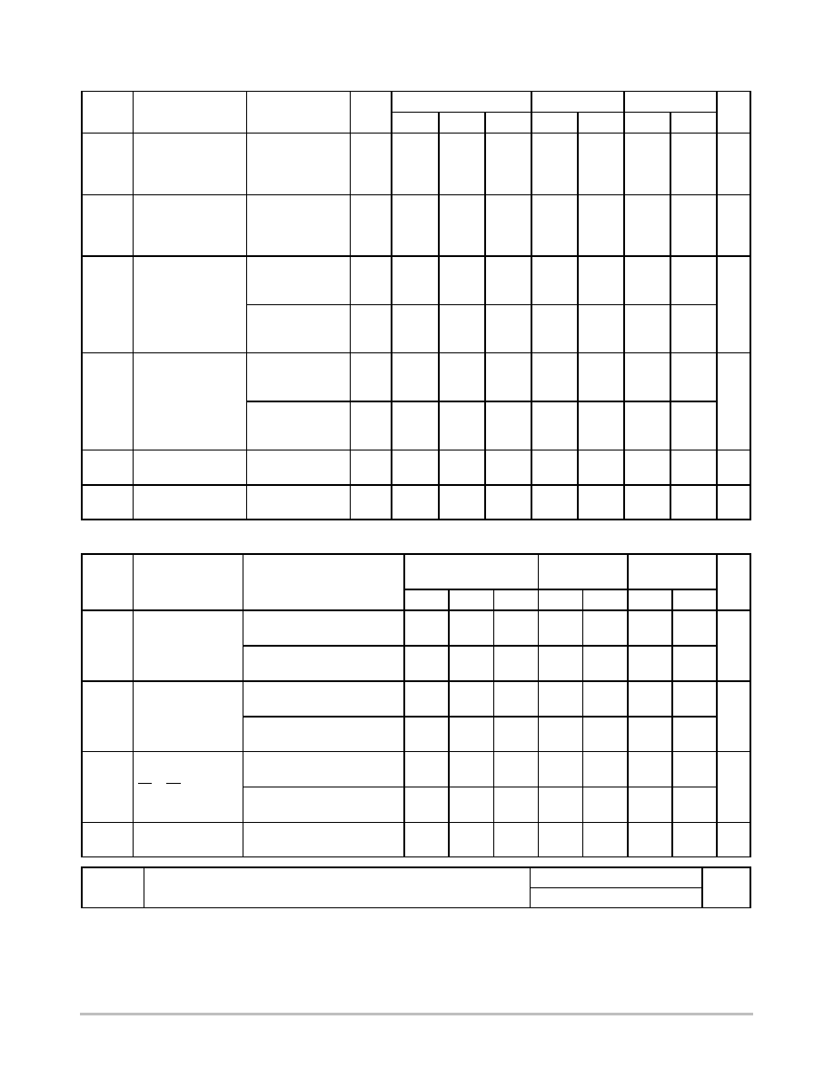
DC ELECTRICAL CHARACTERISTICS
ŒŒŒŒ
ŒŒŒŒ
ŒŒŒŒŒŒ
ŒŒŒŒŒŒ
ŒŒŒŒŒŒ
ŒŒŒŒŒŒ
ŒŒŒ
ŒŒŒ
V
CC
ŒŒŒŒŒŒŒŒ
ŒŒŒŒŒŒŒŒ
T
A
= 25
∞
C
ŒŒŒŒŒ
ŒŒŒŒŒ
T
A
=
85
∞
C
ŒŒŒŒŒŒ
ŒŒŒŒŒŒ
T
A
=
125
∞
C
ŒŒ
ŒŒ
ŒŒŒŒ
ŒŒŒŒ
Symbol
ŒŒŒŒŒŒ
ŒŒŒŒŒŒ
Parameter
ŒŒŒŒŒŒ
ŒŒŒŒŒŒ
Test Conditions
ŒŒŒ
ŒŒŒ
V
CC
(V)
ŒŒŒ
ŒŒŒ
Min
ŒŒŒŒ
ŒŒŒŒ
Typ
ŒŒŒ
ŒŒŒ
Max
ŒŒŒ
ŒŒŒ
Min
ŒŒŒ
ŒŒŒ
Max
ŒŒŒŒ
ŒŒŒŒ
Min
ŒŒŒ
ŒŒŒ
Max
ŒŒ
ŒŒ
Unit
ŒŒŒŒ
Œ
ŒŒ
Œ
Œ
ŒŒ
Œ
ŒŒŒŒ
V
IH
ŒŒŒŒŒŒ
Œ
ŒŒŒŒ
Œ
Œ
ŒŒŒŒ
Œ
ŒŒŒŒŒŒ
Minimum High≠Level
Input Voltage
ŒŒŒŒŒŒ
Œ
ŒŒŒŒ
Œ
Œ
ŒŒŒŒ
Œ
ŒŒŒŒŒŒ
ŒŒŒ
Œ
Œ
Œ
Œ
Œ
Œ
ŒŒŒ
2.0
3.0
4.5
5.5
ŒŒŒ
Œ
Œ
Œ
Œ
Œ
Œ
ŒŒŒ
1.5
2.1
3.15
3.85
ŒŒŒŒ
Œ
ŒŒ
Œ
Œ
ŒŒ
Œ
ŒŒŒŒ
ŒŒŒ
Œ
Œ
Œ
Œ
Œ
Œ
ŒŒŒ
ŒŒŒ
Œ
Œ
Œ
Œ
Œ
Œ
ŒŒŒ
1.5
2.1
3.15
3.85
ŒŒŒ
Œ
Œ
Œ
Œ
Œ
Œ
ŒŒŒ
ŒŒŒŒ
Œ
ŒŒ
Œ
Œ
ŒŒ
Œ
ŒŒŒŒ
1.5
2.1
3.15
3.85
ŒŒŒ
ŒŒ
Œ
ŒŒ
Œ
ŒŒŒ
ŒŒ
ŒŒ
ŒŒ
ŒŒ
V
ŒŒŒŒ
Œ
ŒŒ
Œ
Œ
ŒŒ
Œ
ŒŒŒŒ
V
IL
ŒŒŒŒŒŒ
Œ
ŒŒŒŒ
Œ
Œ
ŒŒŒŒ
Œ
ŒŒŒŒŒŒ
Maximum
Low≠Level Input
Voltage
ŒŒŒŒŒŒ
Œ
ŒŒŒŒ
Œ
Œ
ŒŒŒŒ
Œ
ŒŒŒŒŒŒ
ŒŒŒ
Œ
Œ
Œ
Œ
Œ
Œ
ŒŒŒ
2.0
3.0
4.5
5.5
ŒŒŒ
Œ
Œ
Œ
Œ
Œ
Œ
ŒŒŒ
ŒŒŒŒ
Œ
ŒŒ
Œ
Œ
ŒŒ
Œ
ŒŒŒŒ
ŒŒŒ
Œ
Œ
Œ
Œ
Œ
Œ
ŒŒŒ
0.5
0.9
1.35
1.65
ŒŒŒ
Œ
Œ
Œ
Œ
Œ
Œ
ŒŒŒ
ŒŒŒ
Œ
Œ
Œ
Œ
Œ
Œ
ŒŒŒ
0.5
0.9
1.35
1.65
ŒŒŒŒ
Œ
ŒŒ
Œ
Œ
ŒŒ
Œ
ŒŒŒŒ
ŒŒŒ
ŒŒ
Œ
ŒŒ
Œ
ŒŒŒ
0.5
0.9
1.35
1.65
ŒŒ
ŒŒ
ŒŒ
ŒŒ
V
ŒŒŒŒ
Œ
ŒŒ
Œ
ŒŒŒŒ
V
OH
ŒŒŒŒŒŒ
Œ
ŒŒŒŒ
Œ
ŒŒŒŒŒŒ
Minimum High≠Level
Output Voltage
V
IN
= V
IH
or V
IL
ŒŒŒŒŒŒ
Œ
ŒŒŒŒ
Œ
ŒŒŒŒŒŒ
V
IN
= V
IH
or V
IL
I
OH
= ≠ 50
µ
A
ŒŒŒ
Œ
Œ
Œ
ŒŒŒ
2.0
3.0
4.5
ŒŒŒ
Œ
Œ
Œ
ŒŒŒ
1.9
2.9
4.4
ŒŒŒŒ
Œ
ŒŒ
Œ
ŒŒŒŒ
2.0
3.0
4.5
ŒŒŒ
Œ
Œ
Œ
ŒŒŒ
ŒŒŒ
Œ
Œ
Œ
ŒŒŒ
1.9
2.9
4.4
ŒŒŒ
Œ
Œ
Œ
ŒŒŒ
ŒŒŒŒ
Œ
ŒŒ
Œ
ŒŒŒŒ
1.9
2.9
4.4
ŒŒŒ
ŒŒ
Œ
ŒŒŒ
ŒŒ
ŒŒ
ŒŒ
V
ŒŒŒŒ
Œ
ŒŒ
Œ
ŒŒŒŒ
ŒŒŒŒŒŒ
Œ
ŒŒŒŒ
Œ
ŒŒŒŒŒŒ
ŒŒŒŒŒŒ
Œ
ŒŒŒŒ
Œ
ŒŒŒŒŒŒ
V
IN
= V
IH
or V
IL
I
OH
= ≠4 mA
I
OH
= ≠8 mA
ŒŒŒ
Œ
Œ
Œ
ŒŒŒ
3.0
4.5
ŒŒŒ
Œ
Œ
Œ
ŒŒŒ
2.58
3.94
ŒŒŒŒ
Œ
ŒŒ
Œ
ŒŒŒŒ
ŒŒŒ
Œ
Œ
Œ
ŒŒŒ
ŒŒŒ
Œ
Œ
Œ
ŒŒŒ
2.48
3.80
ŒŒŒ
Œ
Œ
Œ
ŒŒŒ
ŒŒŒŒ
Œ
ŒŒ
Œ
ŒŒŒŒ
2.34
3.66
ŒŒŒ
ŒŒ
Œ
ŒŒŒ
ŒŒ
ŒŒ
ŒŒ
ŒŒŒŒ
Œ
ŒŒ
Œ
Œ
ŒŒ
Œ
ŒŒŒŒ
V
OL
ŒŒŒŒŒŒ
Œ
ŒŒŒŒ
Œ
Œ
ŒŒŒŒ
Œ
ŒŒŒŒŒŒ
Maximum
Low≠Level Output
Voltage
V
V
or V
ŒŒŒŒŒŒ
Œ
ŒŒŒŒ
Œ
Œ
ŒŒŒŒ
Œ
ŒŒŒŒŒŒ
V
IN
= V
IH
or V
IL
I
OL
= 50
µ
A
ŒŒŒ
Œ
Œ
Œ
Œ
Œ
Œ
ŒŒŒ
2.0
3.0
4.5
ŒŒŒ
Œ
Œ
Œ
Œ
Œ
Œ
ŒŒŒ
ŒŒŒŒ
Œ
ŒŒ
Œ
Œ
ŒŒ
Œ
ŒŒŒŒ
0.0
0.0
0.0
ŒŒŒ
Œ
Œ
Œ
Œ
Œ
Œ
ŒŒŒ
0.1
0.1
0.1
ŒŒŒ
Œ
Œ
Œ
Œ
Œ
Œ
ŒŒŒ
ŒŒŒ
Œ
Œ
Œ
Œ
Œ
Œ
ŒŒŒ
0.1
0.1
0.1
ŒŒŒŒ
Œ
ŒŒ
Œ
Œ
ŒŒ
Œ
ŒŒŒŒ
ŒŒŒ
ŒŒ
Œ
ŒŒ
Œ
ŒŒŒ
0.1
0.1
0.1
ŒŒ
ŒŒ
ŒŒ
ŒŒ
V
ŒŒŒŒ
Œ
ŒŒ
Œ
ŒŒŒŒ
ŒŒŒŒŒŒ
Œ
ŒŒŒŒ
Œ
ŒŒŒŒŒŒ
V
IN
= V
IH
or V
IL
ŒŒŒŒŒŒ
Œ
ŒŒŒŒ
Œ
ŒŒŒŒŒŒ
V
IN
= V
IH
or V
IL
I
OL
= 4 mA
I
OL
= 8 mA
ŒŒŒ
Œ
Œ
Œ
ŒŒŒ
3.0
4.5
ŒŒŒ
Œ
Œ
Œ
ŒŒŒ
ŒŒŒŒ
Œ
ŒŒ
Œ
ŒŒŒŒ
ŒŒŒ
Œ
Œ
Œ
ŒŒŒ
0.36
0.36
ŒŒŒ
Œ
Œ
Œ
ŒŒŒ
ŒŒŒ
Œ
Œ
Œ
ŒŒŒ
0.44
0.44
ŒŒŒŒ
Œ
ŒŒ
Œ
ŒŒŒŒ
ŒŒŒ
ŒŒ
Œ
ŒŒŒ
0.52
0.52
ŒŒ
ŒŒ
ŒŒ
ŒŒŒŒ
Œ
ŒŒ
Œ
ŒŒŒŒ
I
IN
ŒŒŒŒŒŒ
Œ
ŒŒŒŒ
Œ
ŒŒŒŒŒŒ
Maximum Input
Leakage Current
ŒŒŒŒŒŒ
Œ
ŒŒŒŒ
Œ
ŒŒŒŒŒŒ
V
IN
= 5.5 V or
GND
ŒŒŒ
Œ
Œ
Œ
ŒŒŒ
0 to
5.5
ŒŒŒ
Œ
Œ
Œ
ŒŒŒ
ŒŒŒŒ
Œ
ŒŒ
Œ
ŒŒŒŒ
ŒŒŒ
Œ
Œ
Œ
ŒŒŒ
±
0.1
ŒŒŒ
Œ
Œ
Œ
ŒŒŒ
ŒŒŒ
Œ
Œ
Œ
ŒŒŒ
±
1.0
ŒŒŒŒ
Œ
ŒŒ
Œ
ŒŒŒŒ
ŒŒŒ
ŒŒ
Œ
ŒŒŒ
±
1.0
ŒŒ
ŒŒ
ŒŒ
µ
A
ŒŒŒŒ
ŒŒŒŒ
I
CC
ŒŒŒŒŒŒ
ŒŒŒŒŒŒ
Maximum Quiescent
Supply Current
ŒŒŒŒŒŒ
ŒŒŒŒŒŒ
V
IN
= V
CC
or GND
ŒŒŒ
ŒŒŒ
5.5
ŒŒŒ
ŒŒŒ
ŒŒŒŒ
ŒŒŒŒ
ŒŒŒ
ŒŒŒ
4.0
ŒŒŒ
ŒŒŒ
ŒŒŒ
ŒŒŒ
40.0
ŒŒŒŒ
ŒŒŒŒ
ŒŒŒ
ŒŒŒ
40.0
ŒŒ
ŒŒ
µ
A
ŒŒŒŒŒŒŒŒŒŒŒŒŒŒŒŒŒŒŒŒŒŒŒŒŒŒŒŒŒŒŒŒŒ
ŒŒŒŒŒŒŒŒŒŒŒŒŒŒŒŒŒŒŒŒŒŒŒŒŒŒŒŒŒŒŒŒŒ
AC ELECTRICAL CHARACTERISTICS
(Input t
r
= t
f
= 3.0ns)
ŒŒŒŒ
Œ
ŒŒ
Œ
ŒŒŒŒ
Symbo
ŒŒŒŒŒŒ
Œ
ŒŒŒŒ
Œ
ŒŒŒŒŒŒ
ŒŒŒŒŒŒŒŒŒ
Œ
ŒŒŒŒŒŒŒ
Œ
ŒŒŒŒŒŒŒŒŒ
ŒŒŒŒŒŒŒ
Œ
ŒŒŒŒŒ
Œ
ŒŒŒŒŒŒŒ
T
A
= 25
∞
C
ŒŒŒŒŒ
Œ
ŒŒŒ
Œ
ŒŒŒŒŒ
T
A
= ≠ 40 to
85
∞
C
ŒŒŒŒŒŒ
Œ
ŒŒŒŒ
Œ
ŒŒŒŒŒŒ
T
A
= ≠ 55 to
125
∞
C
ŒŒ
ŒŒ
ŒŒ
ŒŒŒŒ
ŒŒŒŒ
Symbo
l
ŒŒŒŒŒŒ
ŒŒŒŒŒŒ
Parameter
ŒŒŒŒŒŒŒŒŒ
ŒŒŒŒŒŒŒŒŒ
Test Conditions
ŒŒŒ
ŒŒŒ
Min
ŒŒŒ
ŒŒŒ
Typ
ŒŒŒ
ŒŒŒ
Max
ŒŒŒ
ŒŒŒ
Min
ŒŒŒ
ŒŒŒ
Max
ŒŒŒŒ
ŒŒŒŒ
Min
ŒŒŒ
ŒŒŒ
Max
ŒŒ
ŒŒ
Unit
ŒŒŒŒ
ŒŒŒŒ
t
PLH
,
t
PHL
ŒŒŒŒŒŒ
ŒŒŒŒŒŒ
Maximum
Propagation Delay,
A to Y
ŒŒŒŒŒŒŒŒŒ
ŒŒŒŒŒŒŒŒŒ
V
CC
= 3.3
±
0.3V
C
L
= 15pF
C
L
= 50pF
ŒŒŒ
ŒŒŒ
ŒŒŒ
ŒŒŒ
8.2
10.0
ŒŒŒ
ŒŒŒ
11.4
15.8
ŒŒŒ
ŒŒŒ
1.0
1.0
ŒŒŒ
ŒŒŒ
13.5
18.0
ŒŒŒŒ
ŒŒŒŒ
1.0
1.0
ŒŒŒ
ŒŒŒ
13.5
18.0
ŒŒ
ŒŒ
ns
ŒŒŒŒ
Œ
ŒŒ
Œ
ŒŒŒŒ
ŒŒŒŒŒŒ
Œ
ŒŒŒŒ
Œ
ŒŒŒŒŒŒ
A to Y
ŒŒŒŒŒŒŒŒŒ
Œ
ŒŒŒŒŒŒŒ
Œ
ŒŒŒŒŒŒŒŒŒ
V
CC
= 5.0
±
0.5V
C
L
= 15pF
C
L
= 50pF
ŒŒŒ
Œ
Œ
Œ
ŒŒŒ
ŒŒŒ
Œ
Œ
Œ
ŒŒŒ
5.7
7.2
ŒŒŒ
Œ
Œ
Œ
ŒŒŒ
8.1
10.1
ŒŒŒ
Œ
Œ
Œ
ŒŒŒ
1.0
1.0
ŒŒŒ
Œ
Œ
Œ
ŒŒŒ
9.5
11.5
ŒŒŒŒ
Œ
ŒŒ
Œ
ŒŒŒŒ
1.0
1.0
ŒŒŒ
Œ
Œ
Œ
ŒŒŒ
9.5
11.5
ŒŒ
ŒŒ
ŒŒ
ŒŒŒŒ
Œ
ŒŒ
Œ
ŒŒŒŒ
t
PLH
,
t
PHL
ŒŒŒŒŒŒ
Œ
ŒŒŒŒ
Œ
ŒŒŒŒŒŒ
Maximum
Propagation Delay,
E3 to Y
ŒŒŒŒŒŒŒŒŒ
Œ
ŒŒŒŒŒŒŒ
Œ
ŒŒŒŒŒŒŒŒŒ
V
CC
= 3.3
±
0.3V
C
L
= 15pF
C
L
= 50pF
ŒŒŒ
Œ
Œ
Œ
ŒŒŒ
ŒŒŒ
Œ
Œ
Œ
ŒŒŒ
8.1
10.6
ŒŒŒ
Œ
Œ
Œ
ŒŒŒ
12.8
16.3
ŒŒŒ
Œ
Œ
Œ
ŒŒŒ
1.0
1.0
ŒŒŒ
Œ
Œ
Œ
ŒŒŒ
15.0
18.5
ŒŒŒŒ
Œ
ŒŒ
Œ
ŒŒŒŒ
1.0
1.0
ŒŒŒ
Œ
Œ
Œ
ŒŒŒ
15.0
18.5
ŒŒ
ŒŒ
ŒŒ
ns
ŒŒŒŒ
ŒŒŒŒ
ŒŒŒŒŒŒ
ŒŒŒŒŒŒ
E3 to Y
ŒŒŒŒŒŒŒŒŒ
ŒŒŒŒŒŒŒŒŒ
V
CC
= 5.0
±
0.5V
C
L
= 15pF
C
L
= 50pF
ŒŒŒ
ŒŒŒ
ŒŒŒ
ŒŒŒ
5.6
7.1
ŒŒŒ
ŒŒŒ
8.1
10.1
ŒŒŒ
ŒŒŒ
1.0
1.0
ŒŒŒ
ŒŒŒ
9.5
11.5
ŒŒŒŒ
ŒŒŒŒ
1.0
1.0
ŒŒŒ
ŒŒŒ
9.5
11.5
ŒŒ
ŒŒ
ŒŒŒŒ
Œ
ŒŒ
Œ
ŒŒŒŒ
t
PLH
,
t
PHL
ŒŒŒŒŒŒ
Œ
ŒŒŒŒ
Œ
ŒŒŒŒŒŒ
Maximum
Propagation Delay,
E2 or E1 to Y
ŒŒŒŒŒŒŒŒŒ
Œ
ŒŒŒŒŒŒŒ
Œ
ŒŒŒŒŒŒŒŒŒ
V
CC
= 3.3
±
0.3V
C
L
= 15pF
C
L
= 50pF
ŒŒŒ
Œ
Œ
Œ
ŒŒŒ
ŒŒŒ
Œ
Œ
Œ
ŒŒŒ
8.2
10.7
ŒŒŒ
Œ
Œ
Œ
ŒŒŒ
11.4
14.9
ŒŒŒ
Œ
Œ
Œ
ŒŒŒ
1.0
1.0
ŒŒŒ
Œ
Œ
Œ
ŒŒŒ
13.5
17.0
ŒŒŒŒ
Œ
ŒŒ
Œ
ŒŒŒŒ
1.0
1.0
ŒŒŒ
Œ
Œ
Œ
ŒŒŒ
13.5
17.0
ŒŒ
ŒŒ
ŒŒ
ns
ŒŒŒŒ
Œ
ŒŒ
Œ
ŒŒŒŒ
ŒŒŒŒŒŒ
Œ
ŒŒŒŒ
Œ
ŒŒŒŒŒŒ
E2 or E1 to Y
ŒŒŒŒŒŒŒŒŒ
Œ
ŒŒŒŒŒŒŒ
Œ
ŒŒŒŒŒŒŒŒŒ
V
CC
= 5.0
±
0.5V
C
L
= 15pF
C
L
= 50pF
ŒŒŒ
Œ
Œ
Œ
ŒŒŒ
ŒŒŒ
Œ
Œ
Œ
ŒŒŒ
5.8
7.3
ŒŒŒ
Œ
Œ
Œ
ŒŒŒ
8.1
10.1
ŒŒŒ
Œ
Œ
Œ
ŒŒŒ
1.0
1.0
ŒŒŒ
Œ
Œ
Œ
ŒŒŒ
9.5
11.5
ŒŒŒŒ
Œ
ŒŒ
Œ
ŒŒŒŒ
1.0
1.0
ŒŒŒ
Œ
Œ
Œ
ŒŒŒ
9.5
11.5
ŒŒ
ŒŒ
ŒŒ
ŒŒŒŒ
ŒŒŒŒ
C
IN
ŒŒŒŒŒŒ
ŒŒŒŒŒŒ
Maximum Input
Capacitance
ŒŒŒŒŒŒŒŒŒ
ŒŒŒŒŒŒŒŒŒ
ŒŒŒ
ŒŒŒ
ŒŒŒ
ŒŒŒ
4
ŒŒŒ
ŒŒŒ
10
ŒŒŒ
ŒŒŒ
ŒŒŒ
ŒŒŒ
10
ŒŒŒŒ
ŒŒŒŒ
ŒŒŒ
ŒŒŒ
10
ŒŒ
ŒŒ
pF
Typical @ 25
∞
C, V
CC
= 5.0V
C
PD
Power Dissipation Capacitance (Note 1.)
34
pF
1. C
PD
is defined as the value of the internal equivalent capacitance which is calculated from the operating current consumption without load.
Average operating current can be obtained by the equation: I
CC(OPR
)
= C
PD
V
CC
f
in
+ I
CC
. C
PD
is used to determine the no≠load dynamic
power consumption; P
D
= C
PD
V
CC
2
f
in
+ I
CC
V
CC
.