 | ÐлекÑÑоннÑй компоненÑ: MURS320T3 | СкаÑаÑÑ:  PDF PDF  ZIP ZIP |
Äîêóìåíòàöèÿ è îïèñàíèÿ www.docs.chipfind.ru
©
Semiconductor Components Industries, LLC, 2005
March, 2005 - Rev. 6
1
Publication Order Number:
MURS320T3/D
MURS320T3, MURS340T3,
MURS360T3
Preferred Devices
Surface Mount
Ultrafast Power Rectifiers
This series employs the state-of-the-art epitaxial construction with
oxide passivation and metal overlay contact. Ideally suited for high
voltage, high frequency rectification, or as free wheeling and
protection diodes, in surface mount applications where compact size
and weight are critical to the system.
Features
·
Small Compact Surface Mountable Package with J-Bend Leads
·
Rectangular Package for Automated Handling
·
Highly Stable Oxide Passivated Junction
·
Low Forward Voltage Drop
(0.71 to 1.05 Volts Max @ 3.0 A, T
J
= 150
°
C)
·
Pb-Free Packages are Available
Mechanical Characteristics
·
Case: Epoxy, Molded
·
Epoxy Meets UL 94 V-0 @ 0.125 in
·
Weight: 217 mg (approximately)
·
Finish: All External Surfaces Corrosion Resistant and Terminal
Leads are Readily Solderable
·
Lead and Mounting Surface Temperature for Soldering Purposes:
260
°
C Max. for 10 Seconds
·
Shipped in 16 mm Tape and Reel, 2500 units per reel
·
Polarity: Notch in Plastic Body Indicates Cathode Lead
·
Device Meets MSL1 Requirements
·
ESD Ratings:
Machine Model, C (> 400 V)
Human Body Model, 3B (> 8000 V)
Device
Package
Shipping
ORDERING INFORMATION
SMC
CASE 403
PLASTIC
MURS320T3
SMC
2500/Tape & Reel
ULTRAFAST
RECTIFIERS
3.0 AMPERES
200-600 VOLTS
Preferred devices are recommended choices for future use
and best overall value.
MURS340T3
SMC
2500/Tape & Reel
MURS360T3
SMC
2500/Tape & Reel
MARKING DIAGRAM
U3 = Specific Device Code
x
= D, G, or J
A
= Assembly Location
Y
= Year
WW = Work Week
AYWW
U3x
MURS360T3G
SMC
(Pb-Free)
2500/Tape & Reel
MURS340T3G
SMC
(Pb-Free)
2500/Tape & Reel
MURS320T3G
SMC
(Pb-Free)
2500/Tape & Reel
For information on tape and reel specifications,
including part orientation and tape sizes, please
refer to our Tape and Reel Packaging Specifications
Brochure, BRD8011/D.
http://onsemi.com

MURS320T3, MURS340T3, MURS360T3
http://onsemi.com
2
MAXIMUM RATINGS
Rating
Symbol
MURS320T3
MURS340T3
MURS360T3
Unit
Peak Repetitive Reverse Voltage
Working Peak Reverse Voltage
DC Blocking Voltage
V
RRM
V
RWM
V
R
200
400
600
V
Average Rectified Forward Current
I
F(AV)
3.0 @ T
L
= 140
°
C
4.0 @ T
L
= 130
°
C
3.0 @ T
L
= 130
°
C
4.0 @ T
L
= 115
°
C
3.0 @ T
L
= 130
°
C
4.0 @ T
L
= 115
°
C
A
Non-Repetitive Peak Surge Current
(Surge applied at rated load conditions
halfwave, single phase, 60 Hz)
I
FSM
75
A
Operating Junction Temperature
T
J
*
65 to +175
°
C
Maximum ratings are those values beyond which device damage can occur. Maximum ratings applied to the device are individual stress limit
values (not normal operating conditions) and are not valid simultaneously. If these limits are exceeded, device functional operation is not implied,
damage may occur and reliability may be affected.
THERMAL CHARACTERISTICS
Thermal Resistance, Junction-to-Lead
R
q
JL
11
°
C/W
ELECTRICAL CHARACTERISTICS
Maximum Instantaneous Forward Voltage (Note 1)
(i
F
= 3.0 A, T
J
= 25
°
C)
(i
F
= 4.0 A, T
J
= 25
°
C)
(i
F
= 3.0 A, T
J
= 150
°
C)
v
F
0.875
0.89
0.71
1.25
1.28
1.05
1.25
1.28
1.05
V
Maximum Instantaneous Reverse Current (Note 1)
(Rated dc Voltage, T
J
= 25
°
C)
(Rated dc Voltage, T
J
= 150
°
C)
i
R
5.0
150
10
250
10
250
m
A
Maximum Reverse Recovery Time
(i
F
= 1.0 A, di/dt = 50 A/
m
s)
(i
F
= 0.5 A, i
R
= 1.0 A, I
REC
to 0.25 A)
t
rr
35
25
75
50
75
50
ns
Maximum Forward Recovery Time
(i
F
= 1.0 A, di/dt = 100 A/
m
s, Recovery to 1.0 V)
t
fr
25
50
50
ns
1. Pulse Test: Pulse Width = 300
m
s, Duty Cycle
v
2.0%.
MURS320T3, MURS340T3, MURS360T3
http://onsemi.com
3
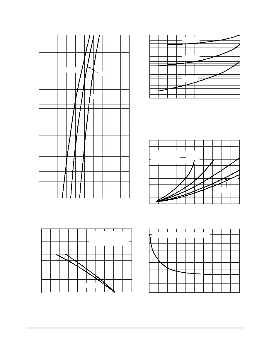
MURS320T3
Figure 1. Typical Forward Voltage
v
F,
INSTANTANEOUS VOLTAGE (VOLTS)
0.3
0.6
0.4
0.8
3.0
0.2
0.1
2.0
0.7
0.7
0.3
0.5
5.0
, INST
ANT
ANEOUS FOR
W
ARD CURRENT
(AMPS)
F
0.9
V
R
, REVERSE VOLTAGE (VOLTS)
0
60
40
100
120
40
80
0.008
0.004
0.002
0.8
0.4
0.2
20
4.0
2.0
8.0
T
J
= 175
°
C
I R
20
80
200
Figure 2. Typical Reverse Current*
T
C
, CASE TEMPERATURE (
°
C)
190
90
1.0
2.0
3.0
4.0
5.0
I F(A
V)
0
6.0
7.0
8.0
9.0
10
100
110
120
130
140
150
160
170
180
I
F(AV)
, AVERAGE FORWARD CURRENT (AMPS)
0
1.5
1.0
0
2.0
1.0
3.0
5.0
4.0
10
7.0
6.0
P
0.5
5.0
Figure 3. Power Dissipation
Figure 4. Current Derating, Case
0
10
20
30
40
60
200
10
20
30
40
100
V
R
, REVERSE VOLTAGE (VOLTS)
Figure 5. Typical Capacitance
0.5
1.0
1.0
1.1
1.2
100
°
C
T
J
= 175
°
C
25
°
C
160
180
140
0.08
0.04
0.02
, REVERSE CURRENT
(
A)
m
T
J
= 100
°
C
T
J
= 25
°
C
3.0
2.5
2.0
4.5
4.0
3.5
9.0
8.0
* The curves shown are typical for the highest voltage device in the
voltage grouping. Typical reverse current for lower voltage selections
can be estimated from these same curves if V
R
is sufficiently below
rated V
R
.
RATED VOLTAGE APPLIED
R
qJL
= 11
°
C/W
T
J
= 175
°
C
C, CAP
ACIT
ANCE (pF)
SQUARE WAVE
dc
,
A
VERAGE FOR
W
ARD CURRENT
(AMPS)
TYPICAL CAPACITANCE AT 0 V = 135 pF
dc
SQUARE WAVE
(CAPACITIVE LOAD)
I
PK
I
AV
+ 20
10
5.0
i
,
A
VERAGE POWER DISSIP
A
TION (W
A
TTS)
F(A
V)
50
60
70
80
90
80
100
0.2
MURS320T3, MURS340T3, MURS360T3
http://onsemi.com
4
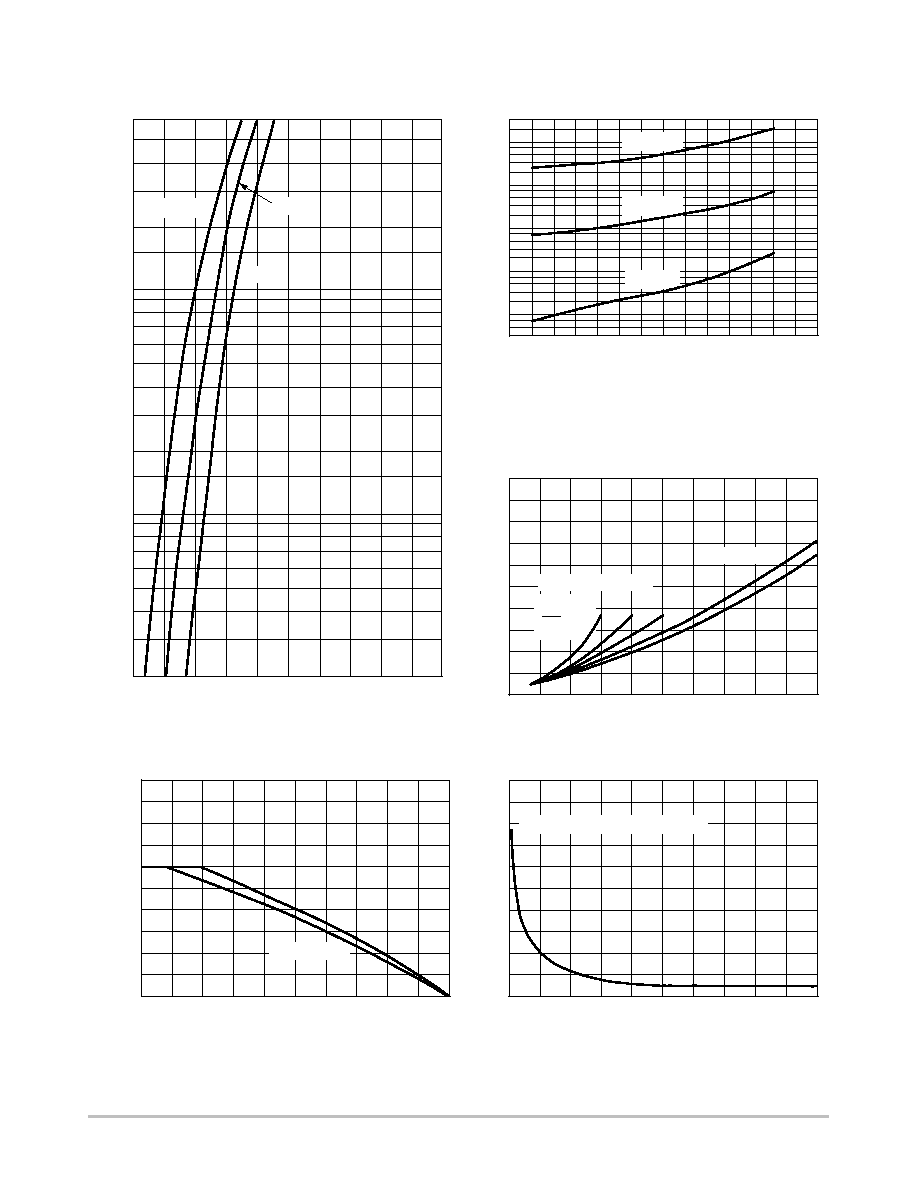
MURS340T3, MURS360T3
Figure 6. Typical Forward Voltage
v
F,
INSTANTANEOUS VOLTAGE (VOLTS)
0.5
1.1
0.7
1.5
3.0
0.05
0.02
2.0
0.7
1.3
0.07
0.5
5.0
, INST
ANT
ANEOUS FOR
W
ARD CURRENT
(AMPS)
F
1.7
V
R
, REVERSE VOLTAGE (VOLTS)
0
300
200
400
40
80
0.008
0.004
0.8
0.4
0.2
20
4.0
2.0
8.0
T
J
= 175
°
C
I R
100
700
Figure 7. Typical Reverse Current*
T
C
, CASE TEMPERATURE (
°
C)
90
1.0
2.0
3.0
4.0
5.0
I F(A
V)
0
6.0
7.0
8.0
9.0
10
100
110
120
130
140
150
160
170
I
F(AV)
, AVERAGE FORWARD CURRENT (AMPS)
0
1.5
1.0
0
2.0
1.0
3.0
5.0
4.0
10
7.0
6.0
P
0.5
5.0
Figure 8. Power Dissipation
Figure 9. Current Derating, Case
0
10
20
30
40
60
0
20
30
40
100
V
R
, REVERSE VOLTAGE (VOLTS)
Figure 10. Typical Capacitance
0.9
1.0
1.9
2.1
2.3
100
°
C
T
J
= 175
°
C
25
°
C
600
500
0.08
0.04
0.02
, REVERSE CURRENT
(
A)
m
T
J
= 100
°
C
T
J
= 25
°
C
3.0
2.5
2.0
4.5
4.0
3.5
9.0
8.0
* The curves shown are typical for the highest voltage device in the
voltage grouping. Typical reverse current for lower voltage selections
can be estimated from these same curves if V
R
is sufficiently below
rated V
R
.
C, CAP
ACIT
ANCE (pF)
SQUARE WAVE
dc
,
A
VERAGE FOR
W
ARD CURRENT
(AMPS)
TYPICAL CAPACITANCE AT 0 V = 75 pF
dc
SQUARE WAVE
10
5.0
i
,
A
VERAGE POWER DISSIP
A
TION (W
A
TTS)
F(A
V)
50
60
70
80
90
80
100
0.3
0.03
0.1
400
200
10
50
70
90
70
80
0.3
0.2
(CAPACITIVE LOADS)
I
PK
I
AV
+ 20
MURS320T3, MURS340T3, MURS360T3
http://onsemi.com
5
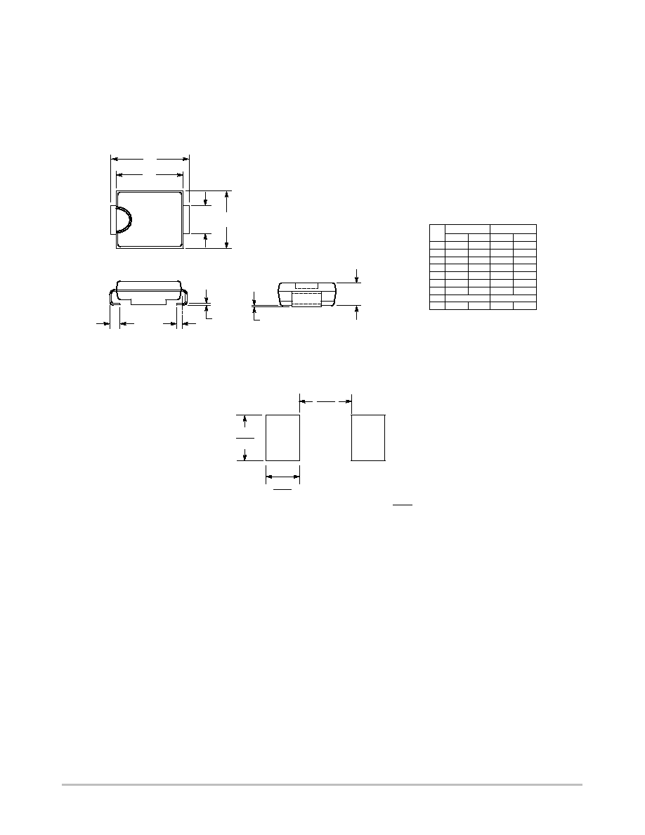
PACKAGE DIMENSIONS
SMC
PLASTIC PACKAGE
CASE 403-03
ISSUE D
*For additional information on our Pb-Free strategy and soldering
details, please download the ON Semiconductor Soldering and
Mounting Techniques Reference Manual, SOLDERRM/D.
SOLDERING FOOTPRINT*
S
A
D
B
J
P
K
H
C
DIM
MIN
MAX
MIN
MAX
MILLIMETERS
INCHES
A
0.260
0.280
6.60
7.11
B
0.220
0.240
5.59
6.10
C
0.075
0.095
1.90
2.41
D
0.115
0.121
2.92
3.07
H 0.0020 0.0060
0.051
0.152
J
0.006
0.012
0.15
0.30
K
0.030
0.050
0.76
1.27
P
0.020 REF
0.51 REF
S
0.305
0.320
7.75
8.13
NOTES:
1. DIMENSIONING AND TOLERANCING PER ANSI
Y14.5M, 1982.
2. CONTROLLING DIMENSION: INCH.
3. D DIMENSION SHALL BE MEASURED WITHIN
DIMENSION P.
4. 403-01 THRU -02 OBSOLETE, NEW STANDARD
403-03.
4.343
0.171
2.794
0.110
3.810
0.150
mm
inches
SCALE 4:1