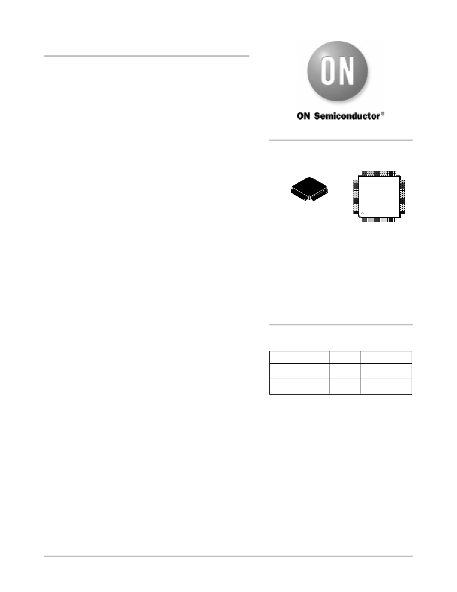
NB100EP223
©
Semiconductor Components Industries, LLC, 2003
June, 2003 - Rev. 5
1
Publication Order Number:
NB100EP223/D
NB100EP223
3.3V 1:22 Differential
HSTL/PECL to HSTL Clock
Driver with LVTTL Clock
Select and Output Enable
The NB100EP223 is a low skew 1-to-22 differential clock driver,
designed with clock distribution in mind, accepting two clock sources
into an input multiplexer. The part is designed for use in low voltage
applications which require a large number of outputs to drive precisely
aligned low skew signals to their destination. The two clock inputs are
differential HSTL or LVPECL and they are selected by the CLK_SEL
pin which is LVTTL. To avoid generation of a runt clock pulse when
the device is enabled/disabled, the Output Enable (OE), which is
LVTTL, is synchronous ensuring the outputs will only be
enabled/disabled when they are already in LOW state (See Figure 7).
The NB100EP223 guarantees low output-to-output skew. The
optimal design, layout, and processing minimize skew within a device
and from lot to lot. In any differential output pair, the same bias and
termination scheme is required. Unused output pairs should be left
unterminated (open) to "reduce power and switching noise as much as
possible." Any unused single line of a differential pair should be
terminated the same as the used line to maintain balanced loads on the
differential driver outputs. The output structure uses an open emitter
architecture and will be terminated with 50
W to ground instead of a
standard HSTL configuration (See Figure 6). The wide VIHCMR
specification allows both pair of CLOCK inputs to accept LVDS
levels.
·
100 ps Typical Device-to- Device Skew
·
25 ps Typical Within Device Skew
·
HSTL Compatible Outputs Drive 50
W to Ground With No
Offset Voltage
·
Maximum Frequency >500 MHz
·
1 ns Typical Propagation Delay
·
LVPECL and HSTL Mode Operating Range: V
CC
= 3 V to 3.6 V
with GND = 0 V, V
CCO
= 1.6 V to 2.0 V
·
Q Output will Default Low with Inputs Open
·
Thermally Enhanced 64-Lead LQFP
·
CLOCK Inputs are LVDS-Compatible; Requires External 100
W
LVDS Termination Resistor
64-LEAD LQFP
CASE 848G
THERMALLY ENHANCED
FA SUFFIX
Device
Package
Shipping
ORDERING INFORMATION
NB100EP223FA
LQFP-64
160 Units/Tray
NB100EP223FAR2
LQFP-64 1500/Tape & Reel
MARKING
DIAGRAM*
*For additional information, see Application Note
AND8002/D
A
= Assembly Location
WL
= Wafer Lot
YY
= Year
WW
= Work Week
NB100
EP223
AWLYYWW
64
1
64
1
http://onsemi.com
NB100EP223
http://onsemi.com
2
49
50
51
52
53
54
55
56
31
30
29
28
27
26
25
1
2
3
4
5
6
7
8
48
47
46
45
44
43
42
41
32
All V
CC
, V
CCO
, and GND pins must be externally connected to appropriate Power Supply to guarantee proper operation (V
CC
0
V
CCO
).
The thermally conductive exposed pad on package bottom (see package case drawing) is electrically connected to GND internally.
FUNCTION TABLE
OE*
L
L
H
H
PIN DESCRIPTION
FUNCTION
HSTL, LVPECL or LVDS Differential Inputs
LVPECL Differential Inputs
LVCMOS/LVTTL Input CLK Select
LVCMOS/LVTTL Output Enable
HSTL Differential Outputs
Positive Supply_Core (3.0 V - 3.6 V)
Positive Supply_HSTL Outputs(1.6V-2.0V)
Ground
PIN
HSTL_CLK*, HSTL_CLK**
LVPECL_CLK*, LVPECL_CLK**
CLK_SEL**
OE**
Q0-Q21, Q0-Q21
V
CC
V
CCO
GND***
Figure 1. 64-Lead LQFP Pinout (Top View)
V
CC0
HSTL_CLK
HSTL_CLK
CLK_SEL
L
VPECL_CLK
L
VPECL_CLK
GND
OE
V
CCO
V
CCO
Q7
Q7
Q8
Q8
Q9
Q9
Q6
V
CC0
Q6
Q5
Q5
Q4
Q0
V
CC0
V
CC0
Q14
Q14
Q15
Q15
Q16
Q16
V
CC0
CLK_SEL
L
H
L
H
Q0-Q21
Q0-Q21
L
L
HSTL_CLK
LVPECL_CLK
H
H
HSTL_CLK
LVPECL_CLK
* The OE (Output Enable) signal is synchronized with the
rising edge of the HSTL_CLK and LVPECL_CLK signal.
NB100EP223
* Pins will default LOW when left open.
** Pins will default HIGH when left open.
*** The thermally conductive exposed pad on the bottom of the package is electrically connected to GND internally.
9
10
11
12
13
14
15
16
NC
NC
V
CC
NC
NC
V
CC0
Q21
Q21
Q17
Q17
Q18
Q18
Q19
Q19
Q20
Q20
23
22
21
20
19
18
17
24
40
39
38
37
36
35
34
33
57
58
59
60
61
62
63
64
Q10
Q10
Q1
1
Q1
1
Q12
Q12
Q13
Q13
Q4
Q3
Q3
Q2
Q2
Q1
Q1
Q0
NB100EP223
http://onsemi.com
3
0
1
Figure 2. Logic Diagram
CLK_SEL
HSTL_CLK
HSTL_CLK
LVPECL_CLK
LVPECL_CLK
OE
Q0-Q21
(HSTL)
Q0-Q21
(HSTL)
Q
D
22
22
V
CC
GND
V
CCO
ATTRIBUTES
Characteristics
Value
Internal Input Pulldown Resistor
75 k
W
Internal Input Pullup Resistor
37.5 k
W
ESD Protection
Human Body Model
Machine Model
Charged Device Model
> 2 kV
> 150 V
> 2 kV
Moisture Sensitivity (Note 1)
Level 3
Flammability Rating
Oxygen Index: 28 to 34
UL 94 V-0 @ 0.125 in
Transistor Count
693
Meets or exceeds JEDEC Spec EIA/JESD78 IC Latchup Test
1. For additional information, refer to Application Note AND8003/D.
MAXIMUM RATINGS
(Note 2)
Symbol
Parameter
Condition 1
Condition 2
Rating
Units
V
CC
Core Power Supply
GND = 0 V
V
CCO
= 1.8 V
4
V
V
CCO
HSTL Output Power Supply
GND = 0 V
V
CC
= 3.3 V
4
V
V
I
PECL Mode Input Voltage
GND = 0 V
V
I
V
CC
4
V
I
out
Output Current
Continuous
Surge
50
100
mA
mA
T
A
Operating Temperature Range
0 to +85
°
C
T
stg
Storage Temperature Range
-65 to +150
°
C
q
JA
Thermal Resistance (Junction-to-Ambient)
(See Application Information)
0 LFPM
500 LFPM
64 LQFP
64 LQFP
35.6
30
°
C/W
°
C/W
q
JC
Thermal Resistance (Junction-to-Case)
(See Application Information)
0 LFPM
500 LFPM
64 LQFP
64 LQFP
3.2
6.4
°
C/W
°
C/W
T
sol
Wave Solder
< 2 to 3 sec @ 248
°
C
265
°
C
2. Maximum Ratings are those values beyond which device damage may occur.
NB100EP223
http://onsemi.com
4
LVPECL DC CHARACTERISTICS
V
CC
= 3.3 V; V
CCO
= 1.8 V; GND
= 0 V
0
°
C
25
°
C
85
°
C
Symbol
Characteristic
Min
Typ
Max
Min
Typ
Max
Min
Typ
Max
Unit
I
CC
Power Supply Current
V
CC
82
100
130
82
100
130
82
100
130
mA
V
IH
Input HIGH Voltage (Single-Ended)
2135
2420
2135
2420
2135
2420
mV
V
IL
Input LOW Voltage (Single-Ended)
1490
1675
1490
1675
1490
1675
mV
V
IHCMR
Input HIGH Voltage Common Mode
Range (Differential) (Note 3) (Figure 4)
LVPECL_CLK/LVPECL_CLK
HSTL_CLK/HSTL_CLK
1.2
0.3
3.3
1.6
1.2
0.3
3.3
1.6
1.2
0.3
3.3
1.6
V
V
I
IH
Input HIGH Current
150
150
150
m
A
I
IL
Input LOW Current
CLK
CLK
0.5
-150
0.5
-150
0.5
-150
m
A
NOTE:
100EP circuits are designed to meet the DC specifications shown in the above table, after thermal equilibrium has been established.
The circuit is in a test socket or mounted on a printed circuit board and transverse air flow greater than 500 lfpm is maintained.
3. V
IHCMR
min varies 1:1 with V
CC
. The V
IHCMR
range is referenced to the most positive side of the differential input signal.
LVTTL/LVCMOS DC CHARACTERISTICS
V
CC
= 3.3 V; V
CCO
= 1.8 V; GND
= 0 V
0
°
C
25
°
C
85
°
C
Symbol
Characteristic
Min
Typ
Max
Min
Typ
Max
Min
Typ
Max
Unit
V
IH
Input HIGH Voltage
2.0
2.0
2.0
V
V
IL
Input LOW Voltage
0.8
0.8
0.8
V
I
IH
Input HIGH Current
-150
150
-150
150
-150
150
m
A
I
IL
Input LOW Current
-300
300
-300
300
-300
300
m
A
NOTE:
100EP circuits are designed to meet the DC specifications shown in the above table, after thermal equilibrium has been established.
The circuit is in a test socket or mounted on a printed circuit board and transverse air flow greater than 500 lfpm is maintained.
HSTL DC CHARACTERISTICS
V
CC
= 3.3 V; V
CCO
= 1.6-2.0 V; GND
= 0 V
0
°
C
25
°
C
85
°
C
Symbol
Characteristic
Min
Typ
Max
Min
Typ
Max
Min
Typ
Max
Unit
V
OH
Output HIGH Voltage (Note 4)
1000
1200
1000
1200
1000
1200
mV
V
OL
Output LOW Voltage (Note 4)
0
400
0
400
0
400
mV
V
IH
Input HIGH Voltage (Differential)
HSTL_CLK/HSTL_CLK
V
X
+100
1600
V
X
+100
1600
V
X
+100
1600
mV
V
IL
Input LOW Voltage (Differential)
HSTL_CLK/HSTL_CLK
-300
V
X
-100
-300
V
X
-100
-300
V
X
-100
mV
V
X
Differential Cross Point Voltage
680
900
680
900
680
900
mV
I
IH
Input HIGH Current
-150
150
-150
150
-150
150
m
A
I
IL
Input LOW Current
-300
300
-300
300
-300
300
m
A
NOTE:
100EP circuits are designed to meet the DC specifications shown in the above table, after thermal equilibrium has been established.
The circuit is in a test socket or mounted on a printed circuit board and transverse air flow greater than 500 lfpm is maintained.
4. All outputs loaded with 50
W
to GND (See Figure 6).
NB100EP223
http://onsemi.com
5
AC CHARACTERISTICS
V
CC
= 3.0 V to 3.6 V; V
CCO
= 1.6 V to 2.0 V; GND
= 0 V (Note 5)
0
°
C
25
°
C
85
°
C
Symbol
Characteristic
Min
Typ
Max
Min
Typ
Max
Min
Typ
Max
Unit
V
Opp
Differential Output Voltage
(Figure 3)
f
out
< 500 MHz
600
750
600
750
600
700
mV
t
PLH
t
PHL
Propagation Delay (Differential)
LVPECL_CLK to Q
HSTL_CLK to Q
700
800
900
900
1000
1100
750
850
900
950
1100
1200
800
850
1000
1050
1300
1350
ps
ps
t
skew
Within-Device Skew (Note 6)
Device-to-Device Skew (Note 7)
25
100
50
250
30
200
65
450
50
250
115
450
ps
ps
t
JITTER
Random Clock Jitter (Figure 3) (RMS)
0.5
2
0.5
2
0.5
2
ps
V
PP
Input Swing (Differential Mode)
(Note 9) (Figure 4)
LVPECL, HSTL
150
800
1200
150
800
1200
150
800
1200
mV
t
S
OE Set Up Time (Note 8)
1.0
1.0
1.0
ns
t
H
OE Hold Time
0.5
0.5
0.5
ns
t
r
/t
f
Output Rise/Fall Time (20%-80%)
300
450
700
275
450
700
350
500
750
ps
5. Measured with 750 mV (LVPECL) source or 1 V (HSTL) source, 50% duty cycle clock source. All outputs loaded with 50
W
to ground
(See Figure 6).
6. Skew is measured between outputs under identical transitions and conditions on any one device.
7. Device-to-Device skew for identical transitions at identical V
CC
levels.
8. OE Set Up Time is defined with respect to the rising edge of the clock. OE High-to-Low transition ensures outputs remain disabled during
the next clock cycle. OE Low-to-High transition enables normal operation of the next input clock (See Figure 7).
9. V
PP
is the differential input voltage swing required to maintain AC characteristics including t
PD
and device-to-device skew.
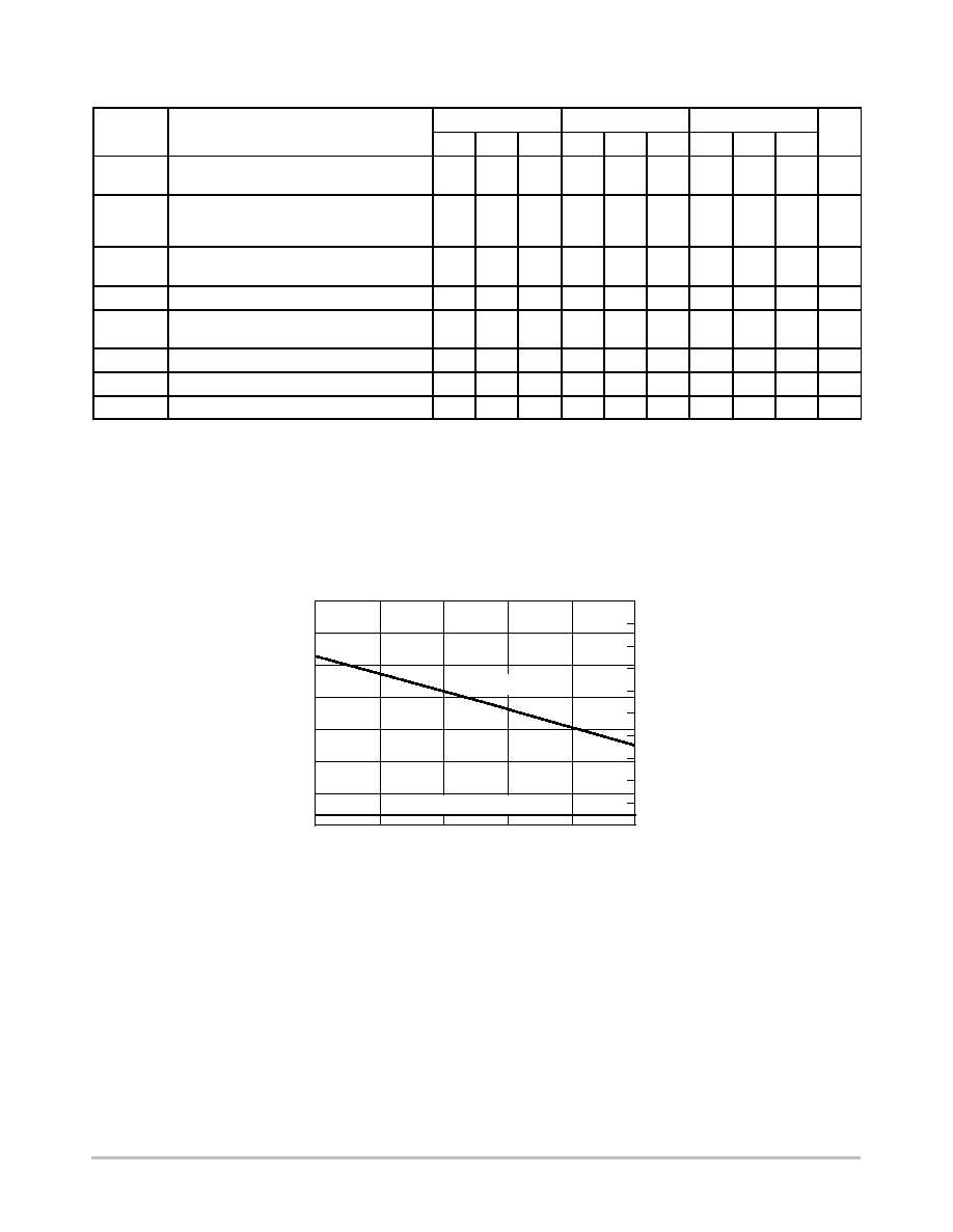
Figure 3. Output Frequency (F
OUT
) versus Output Voltage (V
OPP
) and Random Clock Jitter (t
JITTER
)
FREQUENCY (GHz)
0.5
0.6
0.7
0.8
0.9
1.0
800
900
700
600
500
400
300
200
OUTPUT AMPLITUDE (mV)
9.0
8.0
7.0
6.0
5.0
4.0
3.0
2.0
1.0
0
10
RMS JITTER (ps)
Q AMP (mV)
RMS JITTER (ps)
NB100EP223
http://onsemi.com
6
Figure 4. LVPECL Differential Input Levels
GROUND
HSTL OUTPUT Q
Q
50
W
50
W
V
IH
(DIFF)
V
IL
(DIFF)
GND
V
CC
(LVPECL)
V
IH
(DIFF)
V
IL
(DIFF)
GND
V
CCO
(HSTL)
Figure 5. HSTL Differential Input Levels
Figure 6. HSTL Output Termination and AC Test Reference
V
IHCMR
V
PP
V
PP
V
X
Z = 50
W
Figure 7. Output Enable (OE) Timing Diagram
CLK
CLK
OE
Q
Q
Resource Reference of Application Notes
AN1405
-
ECL Clock Distribution Techniques
AND8002
-
Marking and Date Codes
AND8009
-
ECLinPS Plus Spice I/O Model Kit
AND8020
-
Termination of ECL Logic Devices
For an updated list of Application Notes, please see our website at http://onsemi.com.
NB100EP223
http://onsemi.com
7
APPLICATIONS INFORMATION
Using the thermally enhanced package of the
NB100EP223
The NB100EP223 uses a thermally enhanced 64-lead
LQFP package. The package is molded so that a portion of
the leadframe is exposed at the surface of the package
bottom side. This exposed metal pad will provide the low
thermal impedance that supports the power consumption of
the NB100EP223 high-speed bipolar integrated circuit and
will ease the power management task for the system design.
In multilayer board designs, a thermal land pattern on the
printed circuit board and thermal vias are recommended to
maximize both the removal of heat from the package and
electrical performance of the NB100EP223. The size of the
land pattern can be larger, smaller, or even take on a different
shape than the exposed pad on the package. However, the
solderable area should be at least the same size and shape as
the exposed pad on the package. Direct soldering of the
exposed pad to the thermal land will provide an efficient
thermal conduit. The thermal vias will connect the exposed
pad of the package to internal copper planes of the board.
The number of vias, spacing, via diameters and land pattern
design depend on the application and the amount of heat to
be removed from the package.
Maximum thermal and electrical performance is achieved
when an array of vias is incorporated in the land pattern.
The recommended thermal land design for NB100EP223
applications on multi-layer boards comprises a 4 X 4
thermal via array using a 1.2 mm pitch as shown in Figure 8
providing an efficient heat removal path.
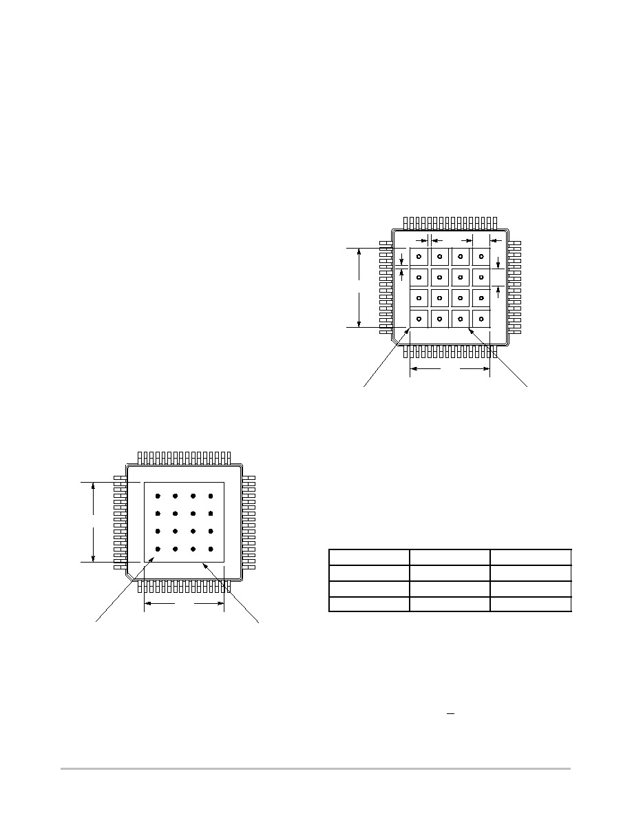
Figure 8. Recommended Thermal Land Pattern
All Units mm
Thermal Via Array (4 X 4)
1.2 mm Pitch
0.3 mm Diameter
Exposed Pad
Land Pattern
4.6
4.6
The via diameter should be approximately 0.3 mm with
1 oz. copper via barrel plating. Solder wicking inside the via
may result in voiding during the solder process and must be
avoided. If the copper plating does not plug the vias, stencil
print solder paste onto the printed circuit pad. This will
supply enough solder paste to fill those vias and not starve
the solder joints. The attachment process for the exposed pad
package is equivalent to standard surface mount packages.
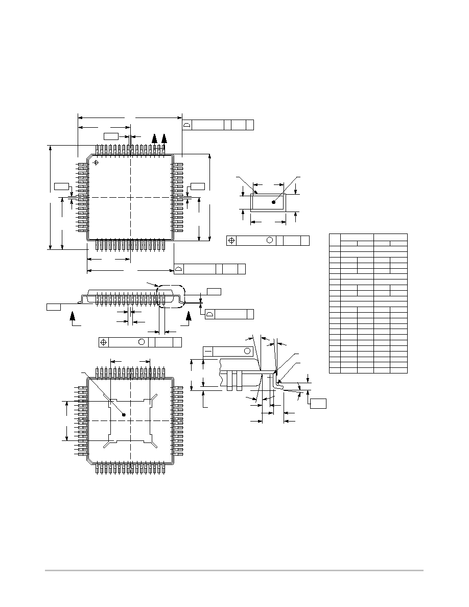
Figure 9, "Recommended solder mask openings", shows a
recommended solder mask opening with respect to a 4 X 4
thermal via array. Because a large solder mask opening may
result in a poor rework release, the opening should be
subdivided as shown in Figure 9. For the nominal package
standoff of 0.1 mm, a stencil thickness of 5 to 8 mils should
be considered.
Figure 9. Recommended Solder Mask Openings
All Units mm
Thermal Via Array (4 X 4)
1.2 mm Pitch
0.3 mm Diameter
Exposed Pad
Land Pattern
4.6
4.6
0.2
1.0
1.0
0.2
Proper thermal management is critical for reliable system
operation. This is especially true for high-fanout and high
output drive capability products.
For thermal system analysis and junction temperature
calculation the thermal resistance parameters of the package
is provided:
Table 1. Thermal Resistance *
LFPM
q
JA
5
C/W
q
JC
5
C/W
0
35.6
3.2
100
32.8
4.9
500
30.0
6.4
* Junction to ambient and Junction to board, four-conductor
layer test board (2S2P) per JESD 51-8
These recommendations are to be used as a guideline,
only. It is therefore recommended that users employ
sufficient thermal modeling analysis to assist in applying the
general recommendations to their particular application to
assure adequate thermal performance. The exposed pad of
the NB100EP223 package is electrically shorted to the
substrate of the integrated circuit and GND. The thermal
land should be electrically connected to GND.
NB100EP223
http://onsemi.com
8
PACKAGE DIMENSIONS
LQFP
FA SUFFIX
64-LEAD PACKAGE
CASE 848G-02
ISSUE A
ÉÉÉÉ
ÉÉÉÉ
ÉÉÉÉ
-Y-
NOTES:
1. DIMENSIONING AND TOLERANCING PER ANSI
Y14.5M, 1982.
2. CONTROLLING DIMENSION: MM.
3. DATUM PLANE E" IS LOCATED AT BOTTOM OF
LEAD AND IS COINCIDENT WITH THE LEAD
WHERE THE LEAD EXITS THE PLASTIC BODY AT
THE BOTTOM OF THE PARTING PLANE.
4. DATUM X", Y" AND Z" TO BE DETERMINED AT
DATUM PLANE DATUM E".
5. DIMENSIONS M AND L TO BE DETERMINED AT
SEATING PLANE DATUM T".
6. DIMENSIONS A AND B DO NOT INCLUDE MOLD
PROTRUSION. ALLOWABLE PROTRUSION IS 0.25
(0.010) PER SIDE. DIMENSIONS A AND B DO
INCLUDE MOLD MISMATCH AND ARE
DETERMINED AT DATUM PLAND E".
7. DIMENSION D DOES NOT INCLUDE DAMBAR
PROTRUSION. ALLOWABLE DAMBAR
PROTRUSION SHALL NOT CAUSE THE LEAD
WIDTH TO EXCEED THE MAXIMUM D DIMENSION
BY MORE THAN 0.08 (0.003). DAMBAR CANNOT
BE LOCATED ON THE LOWER RADIUS OR THE
FOOT. MINIMUM SPACE BETWEEN PROTRUSION
AND ADJACENT LEAD OR PROTRUSION 0.07
(0.003).
8. EXACT SHAPE OF EACH CORNER IS OPTIONAL.
DIM
A
MIN
MAX
MIN
MAX
INCHES
10.00 BSC
0.394 BSC
MILLIMETERS
B
10.00 BSC
0.394 BSC
C
1.35
1.45
0.053
0.057
D
0.17
0.27
0.007
0.011
F
0.45
0.75
0.018
0.030
G
0.50 BSC
0.020 BSC
H
1.00 REF
0.039 BSC
J
0.09
0.20
0.004
0.008
K
0.05
0.15
0.002
0.006
L
12.00 BSC
0.472 BSC
M
12.00 BSC
0.472 BSC
N
0.20 0.008
P
0
7
0
7
R
0
---
0
---
S
---
1.60
---
0.063
V
W
AA
0.17
0.23
0.007
0.009
AB
0.09
0.16
0.004
0.006
AC
0.08
---
0.003
---
AD
0.08
---
0.003
---
AE
4.50
4.78
0.180
0.188
0.05 (0.002)
S
1
B
B/2
16
17
32
33
48
49
64
-X-
L
L/2
-Z-
M
M/2
A
A/2
AJ
AJ
Z
0.20 (0.008) T X-Y
4 PL
Z
0.20 (0.008) E X-Y
-T-
SEATING
PLANE
G/2
G
4 PL
AG
AG
D
64 PL
Z
0.08 (0.003)
M
T X-Y
-E-
0.08 (0.003) T
EXPOSED PAD
VIEW AG-AG
DETAIL AH
DETAIL AH
ÇÇÇÇ
ÇÇÇÇ
_
_
_
_
_
_
AA
D
AB
J
DETAIL AJ-AJ
REF
BASE
METAL
PLATING
Z
0.08 (0.003)
M
Y T-U
S
C
K
V
R
W
N
F
H
P
AC
0.25
GAGE
PLANE
60 PL
1
16
17
32
33
48
49
64
AD
---
---
11
13
11
13
_
_
_
_
11
13
11
13
_
_
_
_
AF
4.50
4.78
0.180
0.188
AE
AF

NB100EP223
http://onsemi.com
9
Notes

NB100EP223
http://onsemi.com
10
ON Semiconductor and are registered trademarks of Semiconductor Components Industries, LLC (SCILLC). SCILLC reserves the right to make
changes without further notice to any products herein. SCILLC makes no warranty, representation or guarantee regarding the suitability of its products for any
particular purpose, nor does SCILLC assume any liability arising out of the application or use of any product or circuit, and specifically disclaims any and all
liability, including without limitation special, consequential or incidental damages. "Typical" parameters which may be provided in SCILLC data sheets and/or
specifications can and do vary in different applications and actual performance may vary over time. All operating parameters, including "Typicals" must be
validated for each customer application by customer's technical experts. SCILLC does not convey any license under its patent rights nor the rights of others.
SCILLC products are not designed, intended, or authorized for use as components in systems intended for surgical implant into the body, or other applications
intended to support or sustain life, or for any other application in which the failure of the SCILLC product could create a situation where personal injury or death
may occur. Should Buyer purchase or use SCILLC products for any such unintended or unauthorized application, Buyer shall indemnify and hold SCILLC
and its officers, employees, subsidiaries, affiliates, and distributors harmless against all claims, costs, damages, and expenses, and reasonable attorney fees
arising out of, directly or indirectly, any claim of personal injury or death associated with such unintended or unauthorized use, even if such claim alleges that
SCILLC was negligent regarding the design or manufacture of the part. SCILLC is an Equal Opportunity/Affirmative Action Employer.
PUBLICATION ORDERING INFORMATION
JAPAN: ON Semiconductor, Japan Customer Focus Center
2-9-1 Kamimeguro, Meguro-ku, Tokyo, Japan 153-0051
Phone: 81-3-5773-3850
ON Semiconductor Website: http://onsemi.com
For additional information, please contact your local
Sales Representative.
NB100EP223/D
Literature Fulfillment:
Literature Distribution Center for ON Semiconductor
P.O. Box 5163, Denver, Colorado 80217 USA
Phone: 303-675-2175 or 800-344-3860 Toll Free USA/Canada
Fax: 303-675-2176 or 800-344-3867 Toll Free USA/Canada
Email: ONlit@hibbertco.com
N. American Technical Support: 800-282-9855 Toll Free USA/Canada