©
Semiconductor Components Industries, LLC, 2006
March, 2006 - Rev. 0
1
Publication Order Number:
NB3L553/D
NB3L553
2.5 V / 3.3 V / 5.0 V
1:4 Clock Fanout Buffer
Description
The NB3L553 is a low skew 1-to 4 clock fanout buffer, designed for
clock distribution in mind. The NB3L553 specifically guarantees low
output-to-output skew. Optimal design, layout and processing
minimize skew within a device and from device to device.
The output enable (OE) pin tri-states the outputs when low.
Features
∑
Input/Output Clock Frequency up to 200 MHz
∑
Low Skew Outputs (35 ps)
∑
Output Enable Mode Three-States Outputs
∑
Operating Range: V
DD
= 2.375 V to 5.25 V
∑
Ideal for Networking Clocks
∑
Packaged in 8-pin SOIC
∑
Industrial Temperature Range
∑
These are Pb-Free Devices
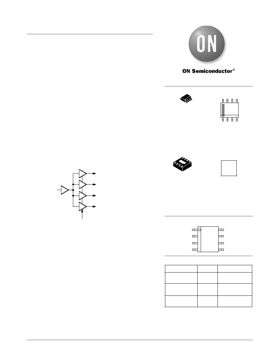
Figure 1. Block Diagram
CLK
Q1
Q2
Q3
Q4
OE
Device
Package
Shipping
ORDERING INFORMATION
NB3L553DG
SOIC-8
(Pb-Free)
98 Units/Rail
SOIC-8
D SUFFIX
CASE 751
MARKING DIAGRAMS*
http://onsemi.com
1
8
3N553 = Specific Device Code
A
= Assembly Location
L
= Wafer Lot
Y
= Year
W
= Work Week
G
= Pb-Free Package
3L553
ALYW
G
1
8
NB3L553DR2G
SOIC-8
(Pb-Free)
2500/Tape & Reel
For information on tape and reel specifications,
including part orientation and tape sizes, please
refer to our Tape and Reel Packaging Specification
Brochure, BRD8011/D.
I
CLK
Q2
Q3
OE
V
DD
Q0
Q1
GND
PINOUT
1
DFN8
MN SUFFIX
CASE 506AA
XX = Specific Device Code
M
= Date Code
XX M
G
G
1
4
NB3L553MNR4G*
DFN-8
(Pb-Free)
1000/Tape & Reel
(Note: Microdot may be in either location)
1
2
3
4
8
7
6
5
*For additional marking information, refer to
Application Note AND8002/D.
*Contact Sales Representative
NB3L553
http://onsemi.com
2
OE
1
0
Function
Enable
Disable
Table 1. OE, Output Enable Function
PIN DESCRIPTION
Pin #
Name
Type
Description
1
V
DD
Power
Positive supply voltage (2.375 V to 5.25 V)
2
Q0
(LV)CMOS/(LV)TTL Output
Clock Output 0
3
Q1
(LV)CMOS/(LV)TTL Output
Clock Output 1
4
GND
Power
Negative supply voltage; Connect to ground, 0 V
5
ICLK
(LV)CMOS/(LV)TTL Input
Clock Input. 5.0 V tolerant
6
Q2
(LV)CMOS/(LV)TTL Output
Clock Output 2
7
Q3
(LV)CMOS/(LV)TTL Output
Clock Output 3
8
OE
(LV)CMOS/(LV)TTL Input
Output Enable for the clock outputs. Outputs are enabled when HIGH: connect to
V
DD
for normal operation; OE pin has internal pull-up resistor. Three-states out-
puts when LOW.
MAXIMUM RATINGS
Symbol
Parameter
Condition 1
Condition 2
Rating
Units
V
DD
Positive Power Supply
GND = 0 V
-
6.0
V
V
I
Input Voltage
-
-
GND ≠0.5
V
I
V
DD
+ 0.5
V
T
A
Operating Temperature Range, Industrial
-
-
-40 to
+85
_
C
T
stg
Storage Temperature Range
-
-
-65 to +150
_
C
q
JA
Thermal Resistance (Junction-to-Ambient)
0 LFPM
500 LFPM
SOIC-8
190
130
_
C/W
_
C/W
q
JC
Thermal Resistance (Junction-to-Case)
(Note 1)
SOIC-8
41 to 44
_
C/W
Stresses exceeding Maximum Ratings may damage the device. Maximum Ratings are stress ratings only. Functional operation above the
Recommended Operating Conditions is not implied. Extended exposure to stresses above the Recommended Operating Conditions may affect
device reliability.
1. JEDEC standard multilayer board - 2S2P (2 signal, 2 power)
ATTRIBUTES
Characteristic
Value
ESD Protection
Human Body Model
Machine Model
Charged Device Model
> 2 kV
> 150 V
> TBD kV
Moisture Sensitivity, Indefinite Time Out of Drypack (Note 2)
Level 1
Flammability Rating
Oxygen Index: 28 to 34
UL-94 code V-0 @ 0.125 in
Transistor Count
531 Devices
Meets or Exceeds JEDEC Standard EIA/JESD78 IC Latchup Test
2. For additional Moisture Sensitivity information, refer to Application Note AND8003/D.

NB3L553
http://onsemi.com
3
DC CHARACTERISTICS
(V
DD
= 2.375 V to 2.625 V, GND = 0 V, T
A
= -40
∞
C to +85
∞
C) (Note 3)
Symbol
Characteristic
Min
Typ
Max
Unit
I
DD
Power Supply Current @ 135 MHz, No Load
-
25
TBD
mA
V
OH
Output HIGH Voltage ≠ I
OH
= -16 mA
2.0
-
-
V
V
OL
Output LOW Voltage ≠ I
OL
= 16 mA
-
-
0.4
V
V
IH,
I
CLK
Input HIGH Voltage, I
CLK
(V
DD
˜
2)+0.5
-
3.8
V
V
IL,
I
CLK
Input LOW Voltage, I
CLK
-
-
(V
DD
˜
2)-0.5
V
V
IH,
OE
Input HIGH Voltage, OE
1.8
-
V
DD
V
V
IL,
OE
Input LOW Voltage, OE
-
-
0.7
V
ZO
Nominal Output Impedance
-
20
-
W
CIN
Input Capacitance, I
CLK
, OE
-
5.0
-
pF
IOS
Short Circuit Current
-
±
28
-
mA
DC CHARACTERISTICS
(V
DD
= 3.15 V to 3.45 V, GND = 0 V, T
A
= -40
∞
C to +85
∞
C) (Note 3)
Symbol
Characteristic
Min
Typ
Max
Unit
I
DD
Power Supply Current @ 135 MHz, No Load
-
35
TBD
mA
V
OH
Output HIGH Voltage ≠ I
OH
= -25 mA
2.4
-
-
V
V
OL
Output LOW Voltage ≠ I
OL
= 25 mA
-
-
0.4
V
V
OH
Output HIGH Voltage ≠ I
OH
= -12 mA (CMOS level)
V
DD
- 0.4
-
-
V
V
IH,
I
CLK
Input HIGH Voltage, I
CLK
(V
DD
˜
2)+0.7
-
3.8
V
V
IL,
I
CLK
Input LOW Voltage, I
CLK
-
-
(V
DD
˜
2)-0.7
V
V
IH,
OE
Input HIGH Voltage, OE
2.0
-
V
DD
V
V
IL,
OE
Input LOW Voltage, OE
0
-
0.8
V
ZO
Nominal Output Impedance
-
20
-
W
CIN
Input Capacitance, OE
-
5.0
-
pF
IOS
Short Circuit Current
-
±
50
-
mA
DC CHARACTERISTICS
(V
DD
= 4.75 V to 5.25 V, GND = 0 V, T
A
= -40
∞
C to +85
∞
C) (Note 3)
Symbol
Characteristic
Min
Typ
Max
Unit
I
DD
Power Supply Current @ 135 MHz, - No Load
-
45
TBD
mA
V
OH
Output HIGH Voltage ≠ I
OH
= -35 mA
2.4
-
-
V
V
OL
Output LOW Voltage ≠ I
OL
= 35 mA
-
-
0.4
V
V
OH
Output HIGH Voltage ≠ I
OH
= -12 mA (CMOS level)
V
DD
- 0.4
-
-
V
V
IH,
I
CLK
Input HIGH Voltage, I
CLK
(V
DD
˜
2) + 1
-
5.5
V
V
IL,
I
CLK
Input LOW Voltage, I
CLK
-
-
(V
DD
˜
2) - 1
V
V
IH,
OE
Input HIGH Voltage, OE
2.0
-
V
DD
V
V
IL,
OE
Input LOW Voltage, OE
-
-
0.8
V
ZO
Nominal Output Impedance
-
20
-
W
CIN
Input Capacitance, OE
-
5.0
-
pF
IOS
Short Circuit Current
-
±
80
-
mA

NB3L553
http://onsemi.com
4
AC CHARACTERISTICS; V
DD
= 2.5 V
+
5%
(V
DD
= 2.375 V to 2.625 V, GND = 0 V, T
A
= -40
∞
C to +85
∞
C) (Note 3)
Symbol
Characteristic
Min
Typ
Max
Unit
f
in
Input Frequency
-
-
200
MHz
t
r
/t
f
Output rise and fall times; 0.8 V to 2.0 V
-
1.0
1.5
ns
t
pd
Propagation Delay, CLK to Qn (Note 4)
2.2
3.0
5.0
ns
t
skew
Output-to-output skew; (Note 5)
-
35
-
ps
t
skew
Device-to-device skew, (Note 5)
-
-
500
ps
AC CHARACTERISTICS; V
DD
= 3.3 V
+
5%
(V
DD
= 3.15 V to 3.45 V, GND = 0 V, T
A
= -40
∞
C to +85
∞
C) (Note 3)
Symbol
Characteristic
Min
Typ
Max
Unit
f
in
Input Frequency
-
-
200
MHz
t
r
/t
f
Output rise and fall times; 0.8 V to 2.0 V
-
0.6
1.0
ns
t
pd
Propagation Delay, CLK to Qn (Note 4)
2.0
2.4
4.0
ns
t
skew
Output-to-output skew; (Note 5)
-
35
50
ps
t
skew
Device-to-device skew, (Note 5)
-
-
500
ps
AC CHARACTERISTICS; V
DD
= 5.0 V
+
5%
(V
DD
= 4.75 V to 5.25 V, GND = 0 V, T
A
= -40
∞
C to +85
∞
C) (Note 3)
Symbol
Characteristic
Min
Typ
Max
Unit
f
in
Input Frequency
-
-
200
MHz
t
r
/t
f
Output rise and fall times; 0.8 V to 2.0 V
-
0.3
0.7
ns
t
pd
Propagation Delay, CLK to Qn (Note 4)
1.8
2.5
4.0
ns
t
skew
Output-to-output skew; (Note 5)
-
35
-
ps
t
skew
Device-to-device skew, (Note 5)
-
-
500
ps
3. Outputs loaded with external R
L
= 33-
W
series resistor and C
L
= 15 pF to GND for proper operation. Duty cycle out = duty in. A 0.01
m
F
decoupling capacitor should be connected between V
DD
and GND.
4. Measured with rail-to-rail input clock
5. Measured on rising edges at V
DD
˜
2 between any two outputs with equal loading.

NB3L553
http://onsemi.com
5
PACKAGE DIMENSIONS
SOIC-8 NB
CASE 751-07
ISSUE AG
SEATING
PLANE
1
4
5
8
N
J
X 45
_
K
NOTES:
1. DIMENSIONING AND TOLERANCING PER
ANSI Y14.5M, 1982.
2. CONTROLLING DIMENSION: MILLIMETER.
3. DIMENSION A AND B DO NOT INCLUDE
MOLD PROTRUSION.
4. MAXIMUM MOLD PROTRUSION 0.15 (0.006)
PER SIDE.
5. DIMENSION D DOES NOT INCLUDE DAMBAR
PROTRUSION. ALLOWABLE DAMBAR
PROTRUSION SHALL BE 0.127 (0.005) TOTAL
IN EXCESS OF THE D DIMENSION AT
MAXIMUM MATERIAL CONDITION.
6. 751-01 THRU 751-06 ARE OBSOLETE. NEW
STANDARD IS 751-07.
A
B
S
D
H
C
0.10 (0.004)
DIM
A
MIN
MAX
MIN
MAX
INCHES
4.80
5.00
0.189
0.197
MILLIMETERS
B
3.80
4.00
0.150
0.157
C
1.35
1.75
0.053
0.069
D
0.33
0.51
0.013
0.020
G
1.27 BSC
0.050 BSC
H
0.10
0.25
0.004
0.010
J
0.19
0.25
0.007
0.010
K
0.40
1.27
0.016
0.050
M
0
8
0
8
N
0.25
0.50
0.010
0.020
S
5.80
6.20
0.228
0.244
-X-
-Y-
G
M
Y
M
0.25 (0.010)
-Z-
Y
M
0.25 (0.010)
Z
S
X
S
M
_
_
_
_
1.52
0.060
7.0
0.275
0.6
0.024
1.270
0.050
4.0
0.155
mm
inches
SCALE 6:1
*For additional information on our Pb-Free strategy and soldering
details, please download the ON Semiconductor Soldering and
Mounting Techniques Reference Manual, SOLDERRM/D.
SOLDERING FOOTPRINT*

NB3L553
http://onsemi.com
6
PACKAGE DIMENSIONS
DFN8
CASE 506AA-01
ISSUE D
NOTES:
1. DIMENSIONING AND TOLERANCING PER
ASME Y14.5M, 1994 .
2. CONTROLLING DIMENSION: MILLIMETERS.
3. DIMENSION b APPLIES TO PLATED
TERMINAL AND IS MEASURED BETWEEN
0.25 AND 0.30 MM FROM TERMINAL.
4. COPLANARITY APPLIES TO THE EXPOSED
PAD AS WELL AS THE TERMINALS.
«««
«««
«««
«««
A
D
E
B
C
0.10
PIN ONE
2 X
REFERENCE
2 X
TOP VIEW
SIDE VIEW
BOTTOM VIEW
A
L
(A3)
D2
E2
C
C
0.10
C
0.10
C
0.08
8 X
A1
SEATING
PLANE
e/2
e
8 X
K
NOTE 3
b
8 X
0.10 C
0.05 C
A BB
DIM
MIN
MAX
MILLIMETERS
A
0.80
1.00
A1
0.00
0.05
A3
0.20 REF
b
0.20
0.30
D
2.00 BSC
D2
1.10
1.30
E
2.00 BSC
E2
0.70
0.90
e
0.50 BSC
K
0.20
---
L
0.25
0.35
1
4
8
5
ON Semiconductor and are registered trademarks of Semiconductor Components Industries, LLC (SCILLC). SCILLC reserves the right to make changes without further notice
to any products herein. SCILLC makes no warranty, representation or guarantee regarding the suitability of its products for any particular purpose, nor does SCILLC assume any liability
arising out of the application or use of any product or circuit, and specifically disclaims any and all liability, including without limitation special, consequential or incidental damages.
"Typical" parameters which may be provided in SCILLC data sheets and/or specifications can and do vary in different applications and actual performance may vary over time. All
operating parameters, including "Typicals" must be validated for each customer application by customer's technical experts. SCILLC does not convey any license under its patent rights
nor the rights of others. SCILLC products are not designed, intended, or authorized for use as components in systems intended for surgical implant into the body, or other applications
intended to support or sustain life, or for any other application in which the failure of the SCILLC product could create a situation where personal injury or death may occur. Should
Buyer purchase or use SCILLC products for any such unintended or unauthorized application, Buyer shall indemnify and hold SCILLC and its officers, employees, subsidiaries, affiliates,
and distributors harmless against all claims, costs, damages, and expenses, and reasonable attorney fees arising out of, directly or indirectly, any claim of personal injury or death
associated with such unintended or unauthorized use, even if such claim alleges that SCILLC was negligent regarding the design or manufacture of the part. SCILLC is an Equal
Opportunity/Affirmative Action Employer. This literature is subject to all applicable copyright laws and is not for resale in any manner.
PUBLICATION ORDERING INFORMATION
N. American Technical Support: 800-282-9855 Toll Free
USA/Canada
Japan: ON Semiconductor, Japan Customer Focus Center
2-9-1 Kamimeguro, Meguro-ku, Tokyo, Japan 153-0051
Phone: 81-3-5773-3850
NB3L553/D
LITERATURE FULFILLMENT:
Literature Distribution Center for ON Semiconductor
P.O. Box 61312, Phoenix, Arizona 85082-1312 USA
Phone: 480-829-7710 or 800-344-3860 Toll Free USA/Canada
Fax: 480-829-7709 or 800-344-3867 Toll Free USA/Canada
Email: orderlit@onsemi.com
ON Semiconductor Website: http://onsemi.com
Order Literature: http://www.onsemi.com/litorder
For additional information, please contact your
local Sales Representative.