
Publication Order Number:
NBLVEP16VR/D
©
Semiconductor Components Industries, LLC, 2003
December, 2003 - Rev. 2
1
NBLVEP16VR
2.5V/3.3V/5V ECL
Differential Receiver/Driver
with Oscillator Gain Stage
and Enabled High Gain
Outputs
The NBLVEP16VR is an ECL/LVPECL oscillator gain stage with
high-gain output buffers, selectable output enable and a feedback
buffer. The NBLVEP16VR is a solution for crystal oscillators and
SAW-based voltage-controlled oscillators.
∑
Q and Q Outputs have Selectable 4 mA or 8 mA, Self Bias Current
Sources
∑
QHG and QHG have a Selectable 10 mA, Self Bias Current Sources
∑
Synchronous Output Enable of the High-Gain Outputs with
Selectable Disabled State
∑
Selectable LVCMOS/LVTTL or LVPECL Level Input of the Output
Enable Pin
∑
Maximum Frequency > 2.5 GHz Typical
∑
(LV)PECL Mode Operating Range: V
CC
= 2.375 V to 5.5 V with
V
EE
= 0 V
∑
NECL Mode Operating Range: V
CC
= 0 V with
V
EE
= -2.375 V to -5.5 V
∑
Temperature Compensated Inputs and Outputs
∑
Excellent Clock Input Sensitivity
∑
V
BB
Output Supports Current Source/Sink Capability up to a
Robust 1.5 mA
Q
Q
D
D
V
BB
OD_MODE
EN
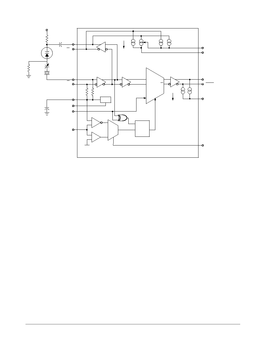
Figure 1. Logic Diagram
CS_SEL
QHG
V
EE
QHG
V
EEP
EN_SEL
Q
Q
0
1
LVCMOS/LVTTL
Threshold
470
W
470
W
10 mA ea. (opt.)
4 mA ea.
4 mA ea. (opt.)
V
BB
V
BB_ADJ
LEN
LATCH
Q
D
Device
Package
Shipping
ORDERING INFORMATION
NBLVEP16VRMN
QFN-16
123 / Rail
NBLVEP16VRMNR2
QFN-16
3000/ Tape &
Reel
QFN-16
MN SUFFIX
CASE 485G
MARKING DIAGRAM
http://onsemi.com
XXXX
XXXX
ALYW
XXXX = Device Code
A
= Assembly Location
L
= Wafer Lot
Y
= Year
W
= Work Week
Bottom View
NBWLVEP16VR
Wafer
Refer to
Note 1.
1. Contact Sales Representative.
For information on tape and reel specifications,
including part orientation and tape sizes, please
refer to our Tape and Reel Packaging Specifications
Brochure, BRD8011/D.

NBLVEP16VR
http://onsemi.com
2
Q
Q
D
D
V
BB
OD_MODE
EN
Figure 2. Logic Diagram
CS_SEL
QHG
V
EE
QHG
V
EEP
EN_SEL
Q
Q
0
1
LVCMOS/LVTTL
Threshold
470
W
470
W
10 mA ea. (opt.)
4 mA ea.
4 mA ea. (opt.)
V
BB
V
BB_ADJ
LEN
LATCH
Q
D
Table 1. Q AND Q INTERNAL CURRENT SOURCE
SELECTOR
CS_SEL
Q
Q
See Figure
OPEN
4 mA Typical
4 mA Typical
13, 13
V
EE
8 mA Typical
8 mA Typical
10, 13
V
CC
0 mA
4 mA Typical
13, 13
Table 2. QHG AND QHG INTERNAL CURRENT
SOURCE SELECTOR
V
EEP
QHG
QHG
See Figure
OPEN
0 mA
0 mA
8, 11
V
EE
10 mA Typical
10 mA Typical
9, 12
Table 3. OUTPUT ENABLE AND OUTPUT DISABLED STATE TRUTH TABLE
EN_SEL
OD-MODE*
EN*
Q and Q
QHG
QHG
V
CC
or OPEN
Low or OPEN
LVPECL Low, V
EE
or OPEN
Data
Data
Data
V
CC
or OPEN
Low or OPEN
LVPECL High or V
CC
Data
Low
High
V
EE
Low or OPEN
LVCMOS Low, V
EE
, or OPEN
Data
Low
High
V
EE
Low or OPEN
LVCMOS High or V
CC
Data
Data
Data
V
CC
or OPEN
High
LVPECL Low, V
EE
or OPEN
Data
Data
Data
V
CC
or OPEN
High
LVPECL High or V
CC
Data
High
Low
V
EE
High
LVCMOS Low, V
EE
, or OPEN
Data
High
Low
V
EE
High
LVCMOS High or V
CC
Data
Data
Data
*Pins will default LOW when left open.
Pin will default HIGH when left open.

NBLVEP16VR
http://onsemi.com
3
Q
Figure 3. Pinout Diagram
(Top View)
D
D
V
BB
OD_MODE
EN
CS_SEL
QHG
V
EE
QHG
V
EEP
EN_SEL
1
2
3
4
5
6
7
8
9
10
11
12
13
14
15
16
V
CC
NC
V
BB_ADJ
NBLVEP16VR
Q
Exposed Pad
(EP)
Q
Figure 4. Die Map
D
D
V
BB
OD_MODE
EN
CS_SEL
QHG
V
EE
QHG
V
EE
EN_SEL
V
CC
NC
V
BB_ADJ
NBLVEP16VR
Die: 1.16 x 1.19 mm
Q
NC
V
BB
V
CC
V
EEP
(x)
(y)
Bond Pad: 84
m
m Diameter
Table 4. PIN DESCRIPTION
Pin No
Name
I/O
Description
1
OD_MODE*
LVCMOS/LVTTL Input (See Table 3)
Selectable Mode of Output Disabled Level
2
D
ECL / LVPECL Input
Clock / Data Input
3
D
ECL / LVPECL Input
Inverted Clock / Data Input
4
V
BB
Reference Voltage Output
Reference Voltage Output
5
EN*
ECL / LVPECL or LVCMOS/LVTTL Input
(see Table 3)
Output Enable Synchronous with D and D
6
V
BB_ADJ
Adjust Standard V
BB
Levels Upward When Tied to V
CC
for
2.5 V Power Supply. Open for 3.3 V and 5 V Power Supply.
7
V
EE
Negative Power Supply
Negative Power Supply
8
V
EEP
Open or Tied to V
EE
(See Table 1) Optional 10mA Current
Source For QHG and QHG
9
EN_SEL
LVCMOS / LVTTL Input (See Table 3)
Input LVEL Selector Pin for EN
10
QHG
ECL / LVPECL Output
Inverted High-Gain Output, Gain > 200
11
QHG
ECL / LVPECL Output
High-Gain Output, Gain > 200
12
CS_SEL
Selects Q and Q Current Source Magnitude (see Table 1),
Open or Tied to V
EE
or V
CC
13
V
CC
Positive Power Supply
Positive Power Supply
14
NC
No Connect
No Connect
15
Q
ECL / LVPECL Output
ECL/LVPECL Output for Feedback Loop
16
Q
ECL / LVPECL Output
Inverted ECL/LVPECL Output for Feedback Loop
EP
¡¡¡¡¡¡¡¡¡¡¡¡¡
¡
¡¡¡¡¡¡¡¡¡¡¡
¡
¡¡¡¡¡¡¡¡¡¡¡¡¡
Power Supply (OPT)
Exposed Pad on Package Bottom Should Only Be Con-
nected to V
EE
or Left Open
*Pins will default LOW when left open.
Pin will default HIGH when left open.
NBLVEP16VR
http://onsemi.com
4
APPLICATIONS INFORMATION
The NBLVEP16VR is an ECL/LVPECL oscillator gain
stage with high-gain output buffers, selectable output
enable and a feedback buffer. The NBLVEP16VR is a
solution for crystal oscillators and SAW-based
voltage-controlled oscillators. Design versatility is
enhanced with EN, a synchronous output enable pin to
eliminate runt pulses; EN_SEL, an input state selector pin
offering LVCMOS/LVTTL or ECL/LVPECL level control
of EN; and OD_MODE, an output disable mode state pin
which selects the polarity of the high-gain output's disabled
state.
The NBLVEP16VR Q and Q outputs are ideal for
feedback applications common in crystal oscillator gain
blocks. They each have a selectable on-chip pull-down
current source. External resistors may be used to increase the
pull-down current to a maximum of 25 mA. The QHG and
QHG outputs each have an optional on-chip pull-down
current source of 10 mA. When V
EEP
is left open, the 10 mA
output current sources are disabled and the QHG and QHG
outputs operate as standard ECL/LVPECL. When V
EEP
is
connected to V
EE
, the 10 mA current sources are activated.
The QHG and QHG pull-down current can be decreased by
using a resistor connect from V
EEP
to V
EE
. See current
source truth table for functions and options.
The output enable input pin, EN, is synchronized with the
D and D data input signals in a way that furnishes glitchless
gating of the QHG and QHG outputs and allows continuous
oscillator operation. For applications that require output
enable control, the NBLVEP16VR provides expanded
output enable selectability. The logic level of the input state
selector pin, EN_SEL, will determine whether the EN pin
accepts ECL/LVPECL or LVCMOS/LVTTL logic levels.
The output disable mode state pin, OD_MODE, adds
functional flexibility by giving the designer a choice of the
QHG outputs' polarity when these high-gain outputs are
disabled. For example, with OD_MODE LOW and
EN LOW (LVPECL), the input is passed to the outputs and
the data output equals the data input. If the D input is LOW
when the EN goes HIGH, the next data transition to a HIGH
is ignored and QHG remains LOW and QHG remains
HIGH. The next positive transition of the data input is not
passed on to the QHG outputs under these conditions. The
QHG and QHG outputs remain in their disabled state as long
as the EN input is held HIGH. The EN input has no influence
on the Q or Q outputs and the data inputs are passed on to
these outputs whether EN is HIGH or LOW. When the data
input is HIGH and EN goes HIGH, it will force QHG LOW
and QHG HIGH on the next negative transition of the D
input. This configuration is ideal for crystal oscillator
applications where the oscillator can be free-running and
QHG/QHG gate on and off synchronously without adding
extra counts to the output. See truth table and timing diagram
for detailed ENable functions and options.
The NBLVEP16VR provides a V
BB
and internal 470
W
bias resistors from D to V
BB
and D to V
BB
for ac coupled
single-ended or differential input signal(s). The V
BB_ADJ
pin is used for 2.5 V single-ended operation when it is
connected to V
CC
. The V
BB
output current source/sink
capability can support a robust 1.5 mA.
For single-ended input conditions, the unused differential
input is internally connected to V
BB
as a switching reference
voltage. Decouple V
BB
and V
CC
with a 0.01
mF capacitor.
This internal V
BB
will rebias AC coupled input(s). Inputs D
or D must be signal driven or auto oscillation may result.
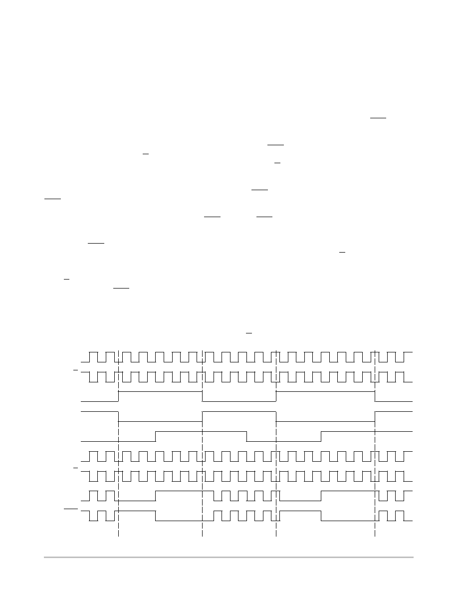
Q
Q
D
OD_MODE
EN
QHG
QHG
D
(PECL)
(CMOS)
EN_SEL HIGH (OPEN)
EN_SEL LOW
(SHORTED TO V
EE
)
Figure 5. Timing Diagram
NBLVEP16VR
http://onsemi.com
5
ATTRIBUTES
Characteristics
Value
ESD Protection
Human Body Model
Machine Model
Charged Device Model
> 2 kV
> 150 V
> 1 kV
Moisture Sensitivity, Indefinite Time Out of Drypack (Note 1)
Level 1
Flammability Rating
Oxygen Index: 28 to 34
UL 94 V-0 @ 0.125 in
Transistor Count
Meets or exceeds JEDEC Spec EIA/JESD78 IC Latchup Test
1. For additional information, see Application Note AND8003/D.
MAXIMUM RATINGS
Symbol
Parameter
Condition 1
Rating
Unit
V
CC
LVPECL Mode Power Supply
V
EE
= 0 V
6
V
V
EE
NECL Mode Power Supply
V
CC
= 0 V
-6
V
V
I
LVPECL Mode Input Voltage
NECL Mode Input Voltage
V
EE
= 0 V
V
CC
= 0 V
6
-6
V
V
I
BB
V
BB
Current Sink/Source
$
1.5
mA
I
IN
Input Current (V
IN
- V
BB
)
B
470
W
D, D
$
5
mA
I
out
Output Current
Continuous
Surge
50
100
mA
mA
T
A
Operating Temperature Range
-40 to +85
∞
C
T
stg
Storage Temperature Range
-65 to +150
∞
C
q
JA
Thermal Resistance (Junction-to-Ambient)
0 LFPM
500 LFPM
∞
C/W
∞
C/W
q
JC
Thermal Resistance (Junction-to-Case)
Standard Board
∞
C/W
Maximum Ratings are those values beyond which damage to the device may occur. Exposure to these conditions or conditions beyond those
indicated may adversely affect device reliability. Functional operation under absolute maximum-rated conditions is not implied. Functional
operation should be restricted to the Recommended Operating Conditions.

NBLVEP16VR
http://onsemi.com
6
DC CHARACTERISTICS, LVPECL
V
CC
= 2.5 V, V
EE
= 0 V (Note 2, 6)
-40
∞
C
25
∞
C
85
∞
C
Symbol
Characteristic
Min
Typ
Max
Min
Typ
Max
Min
Typ
Max
Unit
I
EE
Negative Power Supply Current (Note 3)
30
35
48
30
38
48
35
40
54
mA
V
OH
Output HIGH Voltage (Note 4)
1340
1670
1340
1670
1340
1670
mV
V
OL
Output LOW Voltage (Note 4)
620
950
620
950
620
950
mV
V
IH
Input High Voltage (Single-Ended)
(D, D, EN) (Notes 5, 6)
1655
2000
1655
2000
1655
2000
mV
V
IL
Input Low Voltage (Single-Ended)
(D, D, EN) (Notes 5, 6)
1050
1395
1050
1395
1050
1395
mV
V
BB
Output Voltage Reference (Note 6)
1420
1525
1630
1420
1525
1630
1420
1525
1630
mV
V
IHCMR
Input High Voltage Common Mode Range
(Differential Configuration)
1.2
2.5
1.2
2.5
1.2
2.5
V
I
IH
Input HIGH Current (Note 5)
EN
150
150
150
m
A
I
IL
Input LOW Current (Note 5)
EN
0.5
0.5
0.5
m
A
NOTE:
LVEP circuits are designed to meet the DC specifications shown in the above table after thermal equilibrium has been
established. The circuit is in a test socket or mounted on a printed circuit board and transverse airflow greater than 500 lfpm is
maintained.
2. Input and output parameters vary 1:1 with V
CC
.
3. V
EEP
and CS_SEL open.
4. QHG/QHG outputs loaded with 50
W
to V
CC
- 2.0 V (V
EEP
= OPEN) Figure 11 or with optional current source (V
EEP
= V
EE
) Figure 12.
Q/Q outputs loaded with 8 mA current source (CS_SEL = V
EE
).
5. EN_SEL Open.
6. V
BB_ADJ
tied to V
CC
for 2.5 V single-ended input operation.
DC CHARACTERISTICS, LVPECL
V
CC
= 3.3 V, V
EE
= 0 V (Note 7)
-40
∞
C
25
∞
C
85
∞
C
Symbol
Characteristic
Min
Typ
Max
Min
Typ
Max
Min
Typ
Max
Unit
I
EE
Negative Power Supply Current (Note 8)
30
38
48
30
40
48
35
42
54
mA
V
OH
Output High Voltage (Note 9)
2140
2470
2140
2470
2140
2470
mV
V
OL
Output Low Voltage (Note 9)
1420
1750
1420
1750
1420
1750
mV
V
IH
Input High Voltage (Single-Ended)
(D, D, EN) (Note 10)
2075
2420
2075
2420
2075
2420
mV
V
IL
Input Low Voltage (Single-Ended)
(D, D, EN) (Note 10)
1355
1675
1355
1675
1355
1675
mV
V
BB
Output Voltage Reference
1790
1900
2030
1790
1900
2030
1790
1900
2030
mV
V
IHCMR
Input High Voltage Common Mode Range
(Differential Configuration)
1.2
3.3
1.2
3.3
1.2
3.3
V
I
IH
Input HIGH Current (Note 10)
EN
150
150
150
m
A
I
IL
Input LOW Current (Note 10)
EN
0.5
0.5
0.5
m
A
NOTE:
LVEP circuits are designed to meet the DC specifications shown in the above table after thermal equilibrium has been
established. The circuit is in a test socket or mounted on a printed circuit board and transverse airflow greater than 500 lfpm is
maintained.
7. Input and output parameters vary 1:1 with V
CC
.
8. V
EEP
and CS_SEL open.
9. QHG/QHG outputs loaded with 50
W
to V
CC
- 2.0 V (V
EEP
= OPEN) Figure 11 or with optional current source (V
EEP
= V
EE
) Figure 12.
Q/Q outputs loaded with 8 mA current source (CS_SEL = V
EE
).
10. EN_SEL Open.
NBLVEP16VR
http://onsemi.com
7
DC CHARACTERISTICS, PECL
V
CC
= 5.0 V, V
EE
= 0 V (Note 11)
-40
∞
C
25
∞
C
85
∞
C
Symbol
Characteristic
Min
Typ
Max
Min
Typ
Max
Min
Typ
Max
Unit
I
EE
Negative Power Supply Current (Note 12)
30
41
48
30
43
48
35
45
54
mA
V
OH
Output High Voltage (Note 13)
3840
4170
3840
4170
3840
4170
mV
V
OL
Output Low Voltage (Note 13)
3120
3450
3120
3450
3120
3450
mV
V
IH
Input High Voltage (Single-Ended)
(D, D, EN) (Note 14)
3775
4120
3775
4120
3775
4120
mV
V
IL
Input Low Voltage (Single-Ended)
(D, D, EN) (Note 14)
3055
3375
3055
3375
3055
3375
mV
V
BB
Output Voltage Reference
3490
3600
3730
3490
3600
3730
3490
3600
3730
mV
V
IHCMR
Input High Voltage Common Mode Range
(Differential Configuration)
2.0
5.0
2.0
5.0
2.0
5.0
V
I
IH
Input HIGH Current (Note 14)
EN
150
150
150
m
A
I
IL
Input LOW Current (Note 14)
EN
0.5
0.5
0.5
m
A
NOTE:
LVEP circuits are designed to meet the DC specifications shown in the above table after thermal equilibrium has been
established. The circuit is in a test socket or mounted on a printed circuit board and transverse airflow greater than 500 lfpm is
maintained.
11. Input and output parameters vary 1:1 with V
CC
.
12. V
EEP
and CS_SEL open.
13. QHG/QHG outputs loaded with 50
W
to V
CC
- 2.0 V (V
EEP
= OPEN) Figure 11 or with optional current source (V
EEP
= V
EE
) Figure 12.
Q/Q outputs loaded with 8 mA current source (CS_SEL = V
EE
).
14. EN_SEL Open.
DC CHARACTERISTICS, NECL
V
CC
= 0 V, V
EE
= -5.5V to -2.375 V (Note 15)
-40
∞
C
25
∞
C
85
∞
C
Symbol
Characteristic
Min
Typ
Max
Min
Typ
Max
Min
Typ
Max
Unit
I
EE
Negative Power Supply Current
(Note 16)
30
38
48
30
40
48
35
42
54
mA
V
OH
Output High Voltage (Note 17)
-1160
-830
-1160
-830
-1160
-830
mV
V
OL
Output Low Voltage (Note 17)
-1880
-1550
-1880
-1550
-1880
-1550
mV
V
IH
Input High Voltage (Single-Ended)
(D, D, EN) (Notes 18, 19)
-3.3 V
V
BB_ADJ
= OPEN
-2.5 V
V
BB_ADJ
= V
CC
-1225
-845
-880
-500
-1225
-845
-880
-500
-1225
-845
-880
-500
mV
V
IL
Input Low Voltage (Single-Ended)
(D, D, EN) (Notes 18, 19)
-3.3 V
V
BB_ADJ
= OPEN
-2.5 V
V
BB_ADJ
= V
CC
-1945
-1450
-1625
-1105
-1945
-1450
-1625
-1105
-1945
-1450
-1625
-1105
mV
V
BB
Output Voltage Reference
-3.3 V or -5.2 V
V
BB_ADJ
= OPEN
-2.5 V (Note 19)
V
BB_ADJ
= V
CC
-1510
-1080
-1400
-975
-1270
-870
-1510
-1080
-1400
-975
-1270
-870
-1510
-1080
-1400
-975
-1270
-870
mV
V
IHCMR
Input High Voltage Common Mode
Range (Differential Configuration)
V
EE
v
-5 V
V
EE
+1.2
V
EE
+2.0
0
V
EE
+1.2
V
EE
+2.0
0
V
EE
+1.2
V
EE
+2.0
0
V
V
I
IH
Input HIGH Current (Note 18)
EN
150
150
150
m
A
I
IL
Input LOW Current (Note 18)
EN
0
.5
0.5
0.5
m
A
NOTE:
LVEP circuits are designed to meet the DC specifications shown in the above table after thermal equilibrium has been
established. The circuit is in a test socket or mounted on a printed circuit board and transverse airflow greater than 500 lfpm is
maintained.
15. Input and output parameters vary 1:1 with V
CC
.
16. V
EEP
and CS_SEL open.
17. QHG/QHG outputs loaded with 50
W
to V
CC
- 2.0 V (V
EEP
= OPEN) Figure 11 or with optional current source (V
EEP
= V
EE
) Figure 12.
Q/Q outputs loaded with 8 mA current source (CS_SEL = V
EE
).
18. EN_SEL Open.
19. V
BB_ADJ
tied to V
CC
for -2.5 V single-ended operation.

NBLVEP16VR
http://onsemi.com
8
(LVCMOS/LVTTL DC CHARACTERISTICS
V
CC
= 2.375 V or 5.0 V, V
EE
= 0 V or V
CC
= 0 V, V
EE
= -2.375 V to -5.5 V (Note 20)
-40
∞
C
25
∞
C
85
∞
C
Symbol
Characteristic
Min
Typ
Max
Min
Typ
Max
Min
Typ
Max
Unit
V
IH
Input High Voltage
V
EE
+2.0
V
CC
V
EE
+
2.0
V
CC
V
EE
+2.0
V
CC
V
V
IL
Input Low Voltage
V
EE
V
EE
+0.8
V
EE
V
EE
+0.8
V
EE
V
EE
+0.8
V
I
IH
Input HIGH Current
-150
150
-150
150
-150
150
m
A
I
IL
Input LOW Current
-150
150
-150
150
-150
150
m
A
20. EN_SEL = LOW When EN is Used as a LVCMOS/LVTTL Input.
AC CHARACTERISTICS
V
CC
= 2.375 V to 5.5 V; V
EE
= 0 V or V
CC
= 0 V V
EE
= -2.375 V to -5.5 V (Note 21)
-40
∞
C
25
∞
C
85
∞
C
Symbol
Characteristic
Min
Typ
Max
Min
Typ
Max
Min
Typ
Max
Unit
V
OUTPP
Differential Output (QHG)
f
out
< 1 GHz
Voltage (Peak-to-Peak)
f
out
< 2 GHz
f
out
< 2.5 GHz
500
260
210
660
500
400
500
310
210
700
500
380
500
280
190
700
450
330
mV
mV
t
PLH
,
t
PHL
Propagation Delay (Differential)
Figure 10
D to Q (CS_SEL = OPEN)
Figure 10
D to Q (CS_SEL = V
EE
)
Figure 8
D to QHG (V
EEP
Open)
Figure 9
D to QHG (V
EEP
= V
EE
)
215
155
315
320
290
270
390
400
385
395
475
490
215
165
335
335
300
280
410
415
385
405
495
505
230
205
360
360
315
300
440
450
400
445
520
530
ps
t
S
Set-Up Time
EN to D
0.5
0.5
0.5
ns
t
H
Hold Time
EN to D
1.0
1.0
1.0
ns
t
JITTER
Random Clock Jitter (RMS)
0.5
0.5
0.5
ps
t
SKEW
Duty Cycle Skew (Note 23)
5
20
5
20
5
20
ps
V
INPP
Differential Input Voltage
D to QHG
(Peak-to-Peak) (Note 22)
D to Q
Single-Ended Configuration
D to QHG
25
50
50
800
800
1200
1200
25
50
50
800
800
1200
1200
25
50
50
800
800
1200
1200
mV
mV
mV
t
r
t
f
Output Rise/Fall Times (20% - 80%)
Q, Q (CS_SEL = V
EE
or OPEN)
QHG, QHG (V
EEP
= V
EE
or OPEN)
70
90
120
150
300
210
70
90
120
150
300
210
70
90
120
150
300
210
ps
DC
O
Output Duty Cycle (Note 24) (QHG)
45
50
55
45
50
55
45
50
55
%
21. QHG/QHG and Q/Q outputs loaded with AC coupled 50
W
loads. V
EEP
and CS_SEL connected to V
EE
.
22. V
INPP
is the minimum differential Peak-to-Peak input swing for which AC parameters are guaranteed.
23. Duty cycle skew is defined only for differential operation when the delays are measured from the cross point of the inputs to the cross point
of the outputs, (t
pLH
≠ t
pHL
).
24. Assumes 50% Input Duty Cycle, see Figures 11 or 12.

NBLVEP16VR
http://onsemi.com
9
0
100
200
300
400
500
600
700
800
900
0
500
1000
1500
2000
2500
3000
Figure 6. F
max
/Jitter for QHG, QHG Output
FREQUENCY (MHz)
1
2
3
4
5
6
7
8
V
OUTpp
(mV)
JITTER
OUT
ps (RMS)
9
Differential Inputs
0
100
200
300
400
500
600
700
800
Figure 7. Differential Gain vs. Input Voltage (100 MHz)
V
INPP
(mV)
QHG/QHG
V
OUTpp
(mV)
50
40
30
20
NBLVEP16VR
http://onsemi.com
10
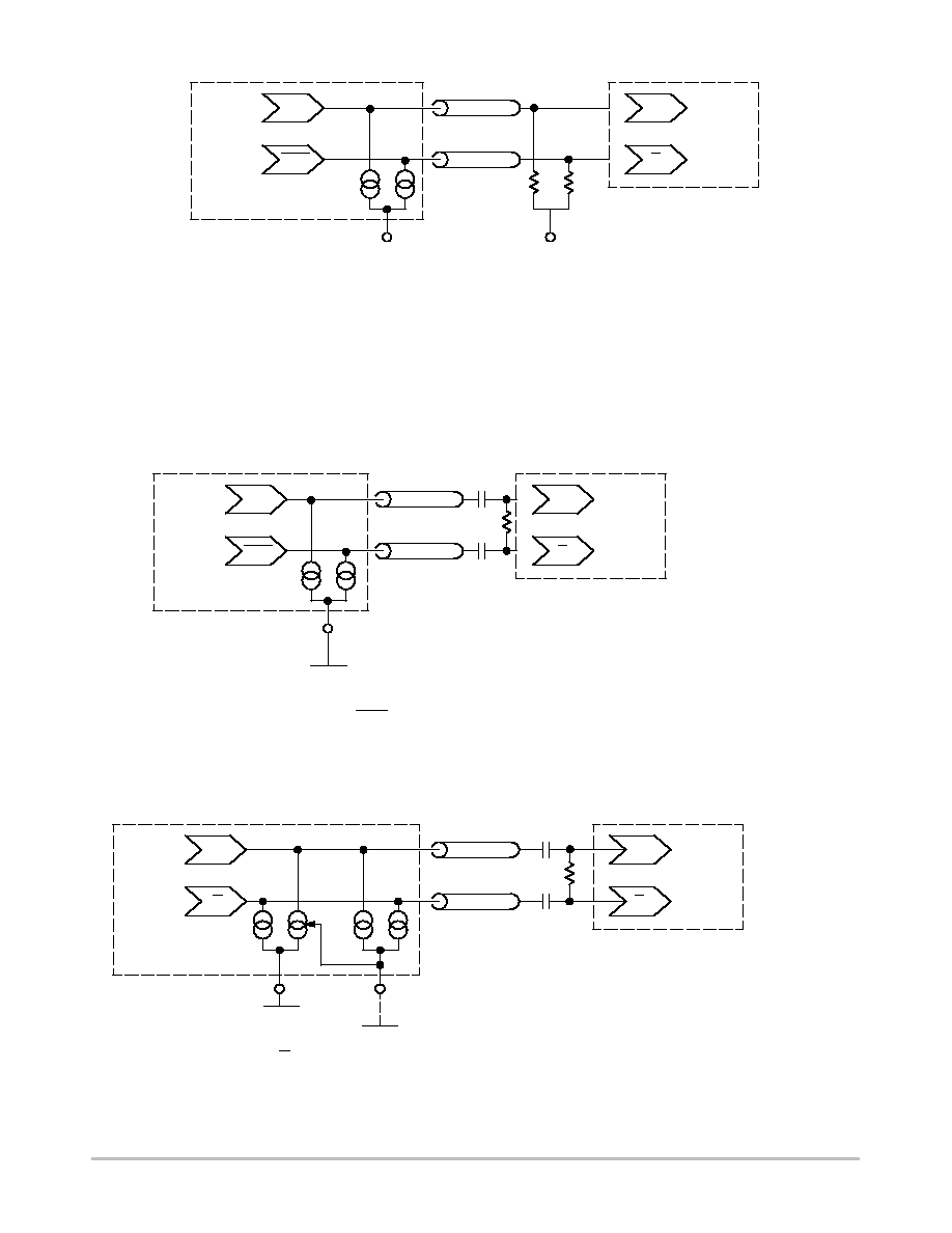
Figure 8. Typical Termination for Output Driver
V
EEP
Open (See Application Note AND8020 - Termination of ECL Logic Devices.)
Figure 9. QHG/QHG Output Loading and Termination, V
EEP
= V
EE
.
Driver
Receiver
Q
D
Q
D
V
EE
*R
Figure 10. Q/Q Output Loading and Termination, CS_SEL Open or Tied to V
EE
or V
CC
Driver
Receiver
QHG
D
QHG
D
CS_SEL (Open or Tied to V
EE
)
*R = 2 Z
o
= 100
W
for 50
W
Transmission
Lines
V
EEP
*R
*R = 2 Z
o
= 100
W
for 50
W
Transmission Lines
V
EE
V
EE
V
EE
Driver
Receiver
QHG
D
QHG
D
V
EEP
(OPEN)
Z
o
= 50
W
V
TT
V
TT
= V
CC
- 2.0 V
50
W
50
W
Z
o
= 50
W
Z
o
= 50
W
Z
o
= 50
W
Z
o
= 50
W
Z
o
= 50
W

NBLVEP16VR
http://onsemi.com
11
Figure 11. QHG/QHG Device Evaluation Set-up; V
EEP
= OPEN
Figure 12. QHG/QHG Device Evaluation Set-up; V
EEP
= V
EE
Driver
Oscilliscope
Q
Q
V
EE
Figure 13. Q/Q Device Evaluation Set-up; CS_SEL = V
EE
or OPEN
Driver
Oscilliscope
QHG
QHG
CS_SEL (Open or Tied to V
EE
)
V
EEP
V
EE
V
EE
V
EE
Driver
Oscilliscope
QHG
QHG
V
EEP
(OPEN)
Z
o
= 50
W
Z
o
= 50
W
Z
o
= 50
W
Z
o
= 50
W
Z
o
= 50
W
Z
o
= 50
W
50
W
50
W
50
W
50
W
50
W
50
W
NBLVEP16VR
http://onsemi.com
12
Q
Q
D
D
V
BB
OD_MODE
EN
CS_SEL
QHG
V
EE
QHG
V
EEP
EN_SEL
Q
Q
0
1
LVCMOS/LVTTL
Threshold
470
W
10 mA ea.
4.0 mA ea.
Figure 14. Typical Application
VR
V
BB_ADJ
V
BB
LEN
LATCH
Q
D
The VCXO, or voltage controlled crystal oscillator, is an
oscillator where the output frequency is controlled by the
crystal and an external control voltage. The VCXO can have
the output frequency change with a change in voltage at a
control pin of the oscillator. Most, if not all, VCXO's use
varactor diodes to vary the frequency. A varactor diode is a
semiconductor device that behaves as a variable capacitor
when a voltage is applied to it. Thus, when a change in the
control voltage is applied to the control pin of the oscillator,
it causes a change in the capacitance seen by the crystal
internal to the oscillator. These changes in the circuit load
capacitance cause changes in the oscillator output frequency
due to crystal loading.

NBLVEP16VR
http://onsemi.com
13
Resource Reference of Application Notes
AN1404
-
ECLinPS Circuit Performance at Non-Standard V
IH
Levels
AN1406
-
Designing with LVPECL (ECL at +5.0 V)
AND8002
-
Marking and Date Codes
AND8009
-
ECLinPS Plus Spice I/O Model Kit
AND8020
-
Termination of ECL Logic Devices
For an updated list of Application Notes, please see our website at http://onsemi.com.

NBLVEP16VR
http://onsemi.com
14
PACKAGE DIMENSIONS
QFN-16
CASE 485G-01
ISSUE A
-T-
-X-
NOTE 3
SEATING
PLANE
L
A
M
-Y-
B
N
0.25 (0.010) T
0.25 (0.010) T
J
C
K
R
0.08 (0.003) T
G
E
H
F
P
D
1
4
5
8
12
9
16
13
DIM
MIN
MAX
MIN
MAX
INCHES
MILLIMETERS
A
3.00 BSC
0.118 BSC
B
3.00 BSC
0.118 BSC
C
0.80
1.00
0.031
0.039
D
0.23
0.28
0.009
0.011
G
0.50 BSC
0.020 BSC
H
0.875
0.925
0.034
0.036
J
0.20 REF
0.008 REF
K
0.00
0.05
0.000
0.002
L
0.35
0.45
0.014
0.018
NOTES:
1. DIMENSIONING AND TOLERANCING PER
ANSI Y14.5M, 1982.
2. CONTROLLING DIMENSION: MILLIMETERS.
3. DIMENSION D APPLIES TO PLATED
TERMINAL AND IS MEASURED BETWEEN
0.25 AND 0.30 MM FROM TERMINAL.
4. COPLANARITY APPLIES TO THE EXPOSED
PAD AS WELL AS THE TERMINALS.
E
1.75
1.85
0.069
0.073
F
1.75
1.85
0.069
0.073
M
1.50 BSC
0.059 BSC
N
1.50 BSC
0.059 BSC
P
0.875
0.925
0.034
0.036
R
0.60
0.80
0.024
0.031
ON Semiconductor and are registered trademarks of Semiconductor Components Industries, LLC (SCILLC). SCILLC reserves the right to make changes without further notice
to any products herein. SCILLC makes no warranty, representation or guarantee regarding the suitability of its products for any particular purpose, nor does SCILLC assume any liability
arising out of the application or use of any product or circuit, and specifically disclaims any and all liability, including without limitation special, consequential or incidental damages.
"Typical" parameters which may be provided in SCILLC data sheets and/or specifications can and do vary in different applications and actual performance may vary over time. All
operating parameters, including "Typicals" must be validated for each customer application by customer's technical experts. SCILLC does not convey any license under its patent rights
nor the rights of others. SCILLC products are not designed, intended, or authorized for use as components in systems intended for surgical implant into the body, or other applications
intended to support or sustain life, or for any other application in which the failure of the SCILLC product could create a situation where personal injury or death may occur. Should
Buyer purchase or use SCILLC products for any such unintended or unauthorized application, Buyer shall indemnify and hold SCILLC and its officers, employees, subsidiaries, affiliates,
and distributors harmless against all claims, costs, damages, and expenses, and reasonable attorney fees arising out of, directly or indirectly, any claim of personal injury or death
associated with such unintended or unauthorized use, even if such claim alleges that SCILLC was negligent regarding the design or manufacture of the part. SCILLC is an Equal
Opportunity/Affirmative Action Employer. This literature is subject to all applicable copyright laws and is not for resale in any manner.
PUBLICATION ORDERING INFORMATION
N. American Technical Support: 800-282-9855 Toll Free
USA/Canada
Japan: ON Semiconductor, Japan Customer Focus Center
2-9-1 Kamimeguro, Meguro-ku, Tokyo, Japan 153-0051
Phone: 81-3-5773-3850
NBLVEP16VR/D
LITERATURE FULFILLMENT:
Literature Distribution Center for ON Semiconductor
P.O. Box 5163, Denver, Colorado 80217 USA
Phone: 303-675-2175 or 800-344-3860 Toll Free USA/Canada
Fax: 303-675-2176 or 800-344-3867 Toll Free USA/Canada
Email: orderlit@onsemi.com
ON Semiconductor Website: http://onsemi.com
Order Literature: http://www.onsemi.com/litorder
For additional information, please contact your
local Sales Representative.