 | –≠–ª–µ–∫—Ç—Ä–æ–Ω–Ω—ã–π –∫–æ–º–ø–æ–Ω–µ–Ω—Ç: NCP345 | –°–∫–∞—á–∞—Ç—å:  PDF PDF  ZIP ZIP |

©
Semiconductor Components Industries, LLC, 2004
December, 2004 - Rev. 5
1
Publication Order Number:
NCP345/D
NCP345
Overvoltage Protection IC
The NCP345 overvoltage protection circuit (OVP) protects
sensitive electronic circuitry from overvoltage transients and power
supply faults when used in conjunction with an external P-channel
FET. The device is designed to sense an overvoltage condition and
quickly disconnect the input voltage supply from the load before any
damage can occur. The OVP consists of a precise voltage reference, a
comparator with hysteresis, control logic, and a MOSFET gate driver.
The OVP is designed on a robust BiCMOS process and is intended to
withstand voltage transients up to 30 V.
The device is optimized for applications that have an external
AC/DC adapter or car accessory charger to power the product and/or
recharge the internal batteries. The nominal overvoltage threshold is
6.85 V so it is suitable for single cell Li-Ion applications as well as 3/4
cell NiCD/NiMH applications.
Features
∑
Overvoltage Turn-Off Time of less than 1.0
msec
∑
Accurate Voltage Threshold of 6.85 V (nominal)
∑
Undervoltage Lockout Protection
∑
CNTRL Input Compatible with 1.8 V Logic Levels
∑
Pb-Free Package is Available
Typical Applications
∑
Cellular Phones
∑
Digital Cameras
∑
Portable Computers and PDAs
∑
Portable CD and other Consumer Electronics
-
+
OUT
IN
V
ref
GND
CNTRL
+
V
CC
Logic
FET
Driver
Undervoltage
Lock Out
LOAD
AC/DC Adapter or
Accessory Charger
C1
Schottky
Diode
Microprocessor port
P-CH
Figure 1. Simplified Application Diagram
NCP345
Note: This device contains 89 active transistors
THIN SOT-23-5
SN SUFFIX
CASE 483
1
5
PIN CONNECTIONS &
MARKING DIAGRAM
1
3
IN
OUT
2
GND
CNTRL
4
VCC
5
(Top View)
Device
Package
Shipping
ORDERING INFORMATION
NCP345SNT1
SOT-23-5
3000 / Tape &
Reel
(7 inch Reel)
RADYW
Y
= Year
W
= Work Week
NCP345SNT1G
SOT-23-5
(Pb-Free)
For information on tape and reel specifications,
including part orientation and tape sizes, please
refer to our Tape and Reel Packaging Specifications
Brochure, BRD8011/D.
http://onsemi.com

NCP345
http://onsemi.com
2
Figure 2. Detailed Block Diagram
-
+
CNTRL
(3)
OUT
(1)
GND
(2)
-
+
LOGIC
BLOCK
DRIVER
Pre-
regulator
V
CC
(5)
IN
(4)
ON/OFF
UVLO
OUT
V5
R1
R2
R3
R4
COMP
Bandgap
Reference
V
CC
V
CC
PIN FUNCTION DESCRIPTIONS
Pin #
Symbol
Pin Description
1
OUT
This signal drives the gate of a P-channel MOSFET. It is controlled by the voltage level on IN or the logic state
of the CNTRL input. When an overvoltage event is detected, the OUT pin is driven to within 1.0 V of V
CC
in
less than 1.0
m
sec provided that gate and stray capacitance is less than 12 nF.
2
GND
Circuit Ground
3
CNTRL
This logic signal is used to control the state of OUT and turn-on/off the P-channel MOSFET. A logic High
results in the OUT signal being driven to within 1.0 V of V
CC
which disconnects the FET. If this pin is not used,
the input should be connected to ground.
4
IN
This pin senses an external voltage point. If the voltage on this input rises above the overvoltage threshold
(VTH), the OUT pin will be driven to within 1.0 V of V
CC
, thus disconnecting the FET. The nominal threshold
level is 6.85 V and this threshold level can be increased with the addition of an external resistor between IN
and V
CC
.
5
V
CC
Positive Voltage supply. If V
CC
falls below 2.8 V (nom), the OUT pin will be driven to within 1.0 V of V
CC
, thus
disconnecting the P-channel FET.
TRUTH TABLE
IN
CNTRL
OUT
<V
th
L
GND
<V
th
H
V
CC
>V
th
L
V
CC
>V
th
H
V
CC

NCP345
http://onsemi.com
3
ABSOLUTE MAXIMUM RATINGS
(T
A
= 25
∞
C unless otherwise noted.)
Rating
Pin
Symbol
Min
Max
Unit
OUT voltage to GND
1
V
O
-0.3
30
V
Input and CNTRL pin voltage to GND
4
3
V
input
V
CNTRL
-0.3
-0.3
30
13
V
V
CC
Maximum Range
5
V
CC(max)
-0.3
30
V
Maximum Power Dissipation at T
A
= 85
∞
C
-
P
D
-
0.216
W
Thermal Resistance Junction to Air
-
R
q
JA
-
300
∞
C/W
Junction Temperature
-
T
J
-
150
∞
C
Operating Ambient Temperature
-
T
A
-40
85
∞
C
V
CNTRL
Operating Voltage
3
-
0
5.0
V
Storage Temperature Range
-
T
stg
-65
150
∞
C
ESD performance (HBM)
{
all
-
2.5
-
kV
Maximum ratings are those values beyond which device damage can occur. Maximum ratings applied to the device are individual stress limit
values (not normal operating conditions) and are not valid simultaneously. If these limits are exceeded, device functional operation is not implied,
damage may occur and reliability may be affected.
{
Human body model (HBM): MIL STD 883C Method 3015-7, (R = 1500 ohms, C = 100 pf, F = 3 pulses delay 1 s).
ELECTRICAL CHARACTERISTICS
(For typical values T
A
= 25
∞
C, for min/max values T
A
= -40
∞
C to +85
∞
C, V
CC
= 6.0 V, unless otherwise noted.)
Characteristic
Symbol
Pin
Min
Typ
Max
Unit
V
CC
Operating Voltage Range
V
CC(opt)
5
3.0
4.8
25
V
Supply Current (I
CC
+ I
Input
; V
CC
= 6.0 V Steady State)
-
4,5
-
0.75
1.0
mA
Input Threshold
(V
Input
connected to V
CC
; V
Input
increasing)
V
Th
4
6.65
6.85
7.08
V
Input Hysteresis (V
Input
connected to V
CC
; V
Input
decreasing)
V
Hyst
4
50
100
200
mV
Input Impedance (Input = V
Th
)
R
in
4
70
150
-
k
W
CNTRL Voltage High
V
ih
3
1.5
-
-
V
CNTRL Voltage Low
V
il
3
-
-
0.5
V
CNTRL Current High (V
ih
= 5.0 V)
I
ih
3
-
95
200
m
A
CNTRL Current Low (V
il
= 0.5 V)
I
il
3
-
10
20
m
A
Undervoltage Lockout (V
CC
decreasing)
V
Lock
3
2.5
2.8
3.0
V
Output Sink Current (V
CC
< V
Th
, V
OUT
= 1.0 V)
I
Sink
1
10
33
50
m
A
Output Voltage High (V
CC
= V
in
= 8.0 V; I
Source
= 10 mA)
Output Voltage High (V
CC
= V
in
= 8.0 V; I
Source
= 0.25 mA)
Output Voltage High (V
CC
= V
in
= 8.0 V; I
Source
= 0 mA)
V
oh
1
V
CC
-1.0
V
CC
-0.25
V
CC
-0.1
-
-
-
-
V
Output Voltage Low
(Input < 6.5 V; I
Sink
= 0 mA; V
CC
= 6.0 V, CNTRL = 0 V)
V
ol
1
-
-
0.1
V
Turn ON Delay - Input (V
Input
connected to V
CC
; V
Input
step down
signal from 8.0 to 6.0 V; measured to 50% point of OUT)*
T
ON IN
1
-
-
10
m
sec
Turn OFF Delay - Input (V
Input
connected to V
CC
; V
Input
step up signal
from 6.0 to 8.0 V; C
L
= 12 nF Output > V
CC
-1.0 V)
T
OFF IN
1
-
0.5
1.0
m
sec
Turn ON Delay - CNTRL (CNTRL step down signal from 2.0 to 0.5 V;
measured to 50% point of OUT)*
T
ON CT
1
-
-
10
m
sec
Turn OFF Delay - CNTRL (CNTRL step up signal from 0.5 to 2.0 V;
C
L
= 12 nF Output > V
CC
-1.0 V)
T
OFF CT
1
-
1.0
2.0
m
sec
*Turn ON Delay is guaranteed by design.
NCP345
http://onsemi.com
4
-40
Ambient Temperature (
∞
C)
-25
-10
5
20
35
50
65
80
95
50
45
40
35
30
25
20
15
10
Sink Current (
m
A)
1.0
0.9
0.8
0.7
0.6
0.5
-40
-25
-10
5
20
35
50
65
80
95
Temperature (
∞
C)
7.05
7.00
6.95
6.90
6.85
6.80
6.75
6.70
-40
-25
-10
5
20
35
50
65
80
95
Ambient Temperature (
∞
C)
V
oltage (V)
I supply
(mA)
V
oltage (V)
50
100 150 200
250
300 350 400
450 500
2
1
0
6
4
2
0
Time (nsec)
T = 25
∞
C
V
LOAD
CNTRL
V
LOAD
= 50
W
MOSFET = MGSF3441
V
oltage (V)
5
10
15
20
25
30
35
40
45
50
2
1
0
6
4
2
0
Time (
m
sec)
T = 25
∞
C
V
LOAD
CNTRL
V
LOAD
= 50
W
MOSFET = MGSF3441
Figure 3. Typical V
th
Threshold Variation vs.
Temperature
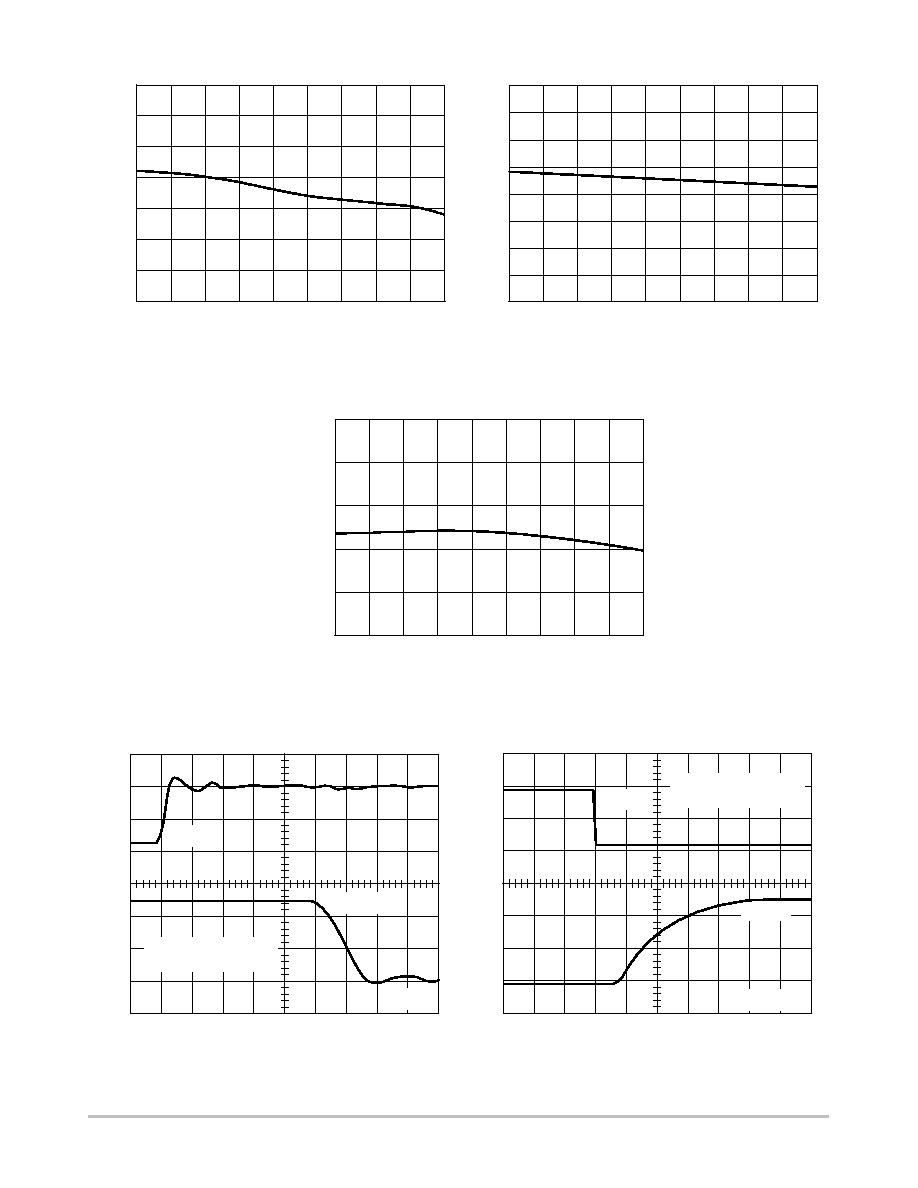
Figure 4. Typical OUT Sink Current vs. Temperature
V
in
t
V
th
, V
out
+
1 V
Figure 5. Typical Supply Current vs. Temperature
I
cc
)
I
in
, V
CC
+
6 V
Figure 6. Typical Turn-off Time CNTRL to V
LOAD
Figure 7. Typical Turn-on Time CNTRL to V
LOAD

NCP345
http://onsemi.com
5
APPLICATION INFORMATION
-
+
OUT
IN
V
ref
GND
CNTRL
+
V
CC
Logic
FET
Driver
Undervoltage
Lock Out
LOAD
AC/DC Adapter or
Accessory Charger
Zener
Diode
(optional)
C1
Schottky
Diode
Microprocessor
port
P-CH
NCP345
Zener
Diode
(optional)
Figure 8.
Introduction
In many electronic products, an external AC/DC wall
adapter is used to convert the AC line voltage into a
regulated DC voltage or a current limited source. Line
surges or faults in the adapter may result in overvoltage
events that can damage sensitive electronic components
within the product. This is becoming more critical as the
operating voltages of many integrated circuits have been
lowered due to advances in sub-micron silicon lithography.
In addition, portable products with removable battery packs
pose special problems since the pack can be removed at any
time. If the user removes a pack in the middle of charging,
a large transient voltage spike can occur which can damage
the product. Finally, damage can result if the user plugs in
the wrong adapter into the charging jack. The challenge of
the product designer is to improve the robustness of the
design and avoid situations where the product can be
damaged due to un-expected, but unfortunately, likely
events that will occur as the product is used.
Circuit Overview
To address these problems, the protection system above
has been developed consisting of the NCP345 Over Voltage
Protection IC and a P-channel MOSFET switch such as the
MGSF3441. The NCP345 monitors the input voltage and
will not turn on the MOSFET unless the input voltage is
within a safe operating window that has an upper limit of
7.05 V. A zener diode can be placed in parallel to the load to
provide for secondary protection during the brief time that
it takes for the NCP345 to detect the overvoltage fault and
disconnect the MOSFET. The decision to use this secondary
diode is a function of the charging currents expected, load
capacitance across the battery, and the desired protection
voltage by analyzing the dV/dT rise that occurs during the
brief time it takes to turn-off the MOSFET. For battery
powered applications, a low-forward voltage Schottky
diode such as the MBRM120LT3 can be placed in series
with the MOSFET to block the body diode of the MOSFET
and prevent shorting the battery out if the input is
accidentally shorted to ground. This provides additional
voltage margin at the load since there is a small forward drop
across this diode that reduces the voltage at the load.
When the protection circuit turns off the MOSFET, there
can be a sudden rise in the input voltage of the device. This
transient can be quite large depending on the impedance of
the supply and the current being drawn from the supply at the
time of an overvoltage event. This inductive spike can be
clamped with a zener diode from IN to ground. This diode
breakdown voltage should be well above the worst case
supply voltage provided from the AC/DC adapter or
Cigarette Lighter Adapter (CLA), since the zener is only
intended to clamp the transient. The NCP345 is designed so
that the IN and V
CC
pin can safely protect up to 25 V and
withstand transients to 30 V. Since these spikes can be very
narrow in duration, it is important to use a high bandwidth
probe and oscilloscope when prototyping the product to
verify the operation of the circuit under all the transient
conditions. A similar problem can result due to contact
bounce as the DC source is plugged into the product.
For portable products it is normal to have a capacitor to
ground in parallel with the battery. If the product has a
battery pack that is easily removable during charging, this
scenario should be analyzed. Under that situation, the
charging current will go into the capacitor and the voltage
may rise rapidly depending on the capacitor value, the
charging current and the power supply response time.

NCP345
http://onsemi.com
6
Normal Operation
Figure 1 illustrates a typical configuration. The external
adapter provides power to the protection system so the
circuitry is only active when the adapter is connected. The
OVP monitors the voltage from the charger and if the
voltage exceeds a nominal voltage of 6.85 V, the OUT signal
drives the gate of the MOSFET to within 1.0 V of V
CC
, thus
turning off the FET and disconnecting the source from the
load. The nominal time it takes to drive the gate to this state
is 400 nsec (1.0 usec maximum for gate capacitance of
< 12 nF). Typical turn off performance using the CNTRL
input can be seen in Figure 6. The CNTRL input can also be
used to interrupt charging and allow the microcontroller to
measure the cell voltage under a normal condition to get a
more accurate measure of the battery voltage. Once the over
voltage is removed, the NCP345 will turn on the MOSFET.
The turn on circuitry is designed to turn on the MOSFET
more gradually to limit the in-rush current. Typical turn-on
performance is illustrated using the MGSF3441 in Figure 7.
This characteristic is a function of the threshold of the
MOSFET and will vary depending on the device
characteristics such as the gate capacitance.
The OVP has an under voltage lockout (UVLO) circuit
which disables the gate driver circuit until the UVLO senses
that the V
CC
voltage is above 2.6 V. Once the UVLO has
released the gate driver circuit, the OUT signal will stay high
until the voltage on the IN is sensed. If the input voltage to
IN is less than 6.85 V nominal, then the OUT signal will be
driven LOW and the FET will be turned on so the source can
be connected to the load.
There are three events that will cause the OVP to drive the
gate of the FET to a HIGH state.
∑
Voltage on V
CC
falls below the UVLO threshold
∑
Voltage on IN rises above 6.85 V (nominal)
∑
CNTRL input is driven to a logic High

NCP345
http://onsemi.com
7
PACKAGE DIMENSIONS
THIN SOT-23-5
SN SUFFIX
CASE 483-02
ISSUE C
THIN SOT-23-5/TSOP-5/SC59-5
0.7
0.028
1.0
0.039
mm
inches
SCALE 10:1
0.95
0.037
2.4
0.094
1.9
0.074
*For additional information on our Pb-Free strategy and soldering
details, please download the ON Semiconductor Soldering and
Mounting Techniques Reference Manual, SOLDERRM/D.
SOLDERING FOOTPRINT*
NOTES:
1. DIMENSIONING AND TOLERANCING PER
ANSI Y14.5M, 1982.
2. CONTROLLING DIMENSION: MILLIMETER.
3. MAXIMUM LEAD THICKNESS INCLUDES
LEAD FINISH THICKNESS. MINIMUM LEAD
THICKNESS IS THE MINIMUM THICKNESS
OF BASE MATERIAL.
4. A AND B DIMENSIONS DO NOT INCLUDE
MOLD FLASH, PROTRUSIONS, OR GATE
BURRS.
DIM
MIN
MAX
MIN
MAX
INCHES
MILLIMETERS
A
2.90
3.10 0.1142 0.1220
B
1.30
1.70 0.0512 0.0669
C
0.90
1.10 0.0354 0.0433
D
0.25
0.50 0.0098 0.0197
G
0.85
1.05 0.0335 0.0413
H
0.013
0.100 0.0005 0.0040
J
0.10
0.26 0.0040 0.0102
K
0.20
0.60 0.0079 0.0236
L
1.25
1.55 0.0493 0.0610
M
0
10
0
10
S
2.50
3.00 0.0985 0.1181
0.05 (0.002)
1
2
3
5
4
S
A
G
L
B
D
H
C
K
M
J
_
_
_
_

NCP345
http://onsemi.com
8
ON Semiconductor and are registered trademarks of Semiconductor Components Industries, LLC (SCILLC). SCILLC reserves the right to make changes without further notice
to any products herein. SCILLC makes no warranty, representation or guarantee regarding the suitability of its products for any particular purpose, nor does SCILLC assume any liability
arising out of the application or use of any product or circuit, and specifically disclaims any and all liability, including without limitation special, consequential or incidental damages.
"Typical" parameters which may be provided in SCILLC data sheets and/or specifications can and do vary in different applications and actual performance may vary over time. All
operating parameters, including "Typicals" must be validated for each customer application by customer's technical experts. SCILLC does not convey any license under its patent rights
nor the rights of others. SCILLC products are not designed, intended, or authorized for use as components in systems intended for surgical implant into the body, or other applications
intended to support or sustain life, or for any other application in which the failure of the SCILLC product could create a situation where personal injury or death may occur. Should
Buyer purchase or use SCILLC products for any such unintended or unauthorized application, Buyer shall indemnify and hold SCILLC and its officers, employees, subsidiaries, affiliates,
and distributors harmless against all claims, costs, damages, and expenses, and reasonable attorney fees arising out of, directly or indirectly, any claim of personal injury or death
associated with such unintended or unauthorized use, even if such claim alleges that SCILLC was negligent regarding the design or manufacture of the part. SCILLC is an Equal
Opportunity/Affirmative Action Employer. This literature is subject to all applicable copyright laws and is not for resale in any manner.
PUBLICATION ORDERING INFORMATION
N. American Technical Support: 800-282-9855 Toll Free
USA/Canada
Japan: ON Semiconductor, Japan Customer Focus Center
2-9-1 Kamimeguro, Meguro-ku, Tokyo, Japan 153-0051
Phone: 81-3-5773-3850
NCP345/D
LITERATURE FULFILLMENT:
Literature Distribution Center for ON Semiconductor
P.O. Box 61312, Phoenix, Arizona 85082-1312 USA
Phone: 480-829-7710 or 800-344-3860 Toll Free USA/Canada
Fax: 480-829-7709 or 800-344-3867 Toll Free USA/Canada
Email: orderlit@onsemi.com
ON Semiconductor Website: http://onsemi.com
Order Literature: http://www.onsemi.com/litorder
For additional information, please contact your
local Sales Representative.