 | –≠–ª–µ–∫—Ç—Ä–æ–Ω–Ω—ã–π –∫–æ–º–ø–æ–Ω–µ–Ω—Ç: NCP4330 | –°–∫–∞—á–∞—Ç—å:  PDF PDF  ZIP ZIP |

©
Semiconductor Components Industries, LLC, 2005
August, 2005 - Rev. 0
1
Publication Order Number:
NCP4330/D
NCP4330
Post Regulation Driver
The NCP4330 houses a dual MOSFET driver intended to be used as
a companion chip in AC-DC or DC-DC multi-output post regulated
power supplies. Being directly fed by the secondary AC signal, the
device keeps power dissipation to the lowest while reducing the
surrounding part count. Furthermore, the implementation of a
N-channel MOSFET gives NCP4330-based applications a significant
advantage in terms of efficiency.
Features
∑
Undervoltage Lockout
∑
Thermal Shutdown for Overtemperature Protection
∑
PWM Operation Synchronized to the Converter Frequency
∑
High Gate Drive Capability
∑
Bootstrap for N-MOSFET High-Side Drive
∑
Over-Lap Management for Soft Switching
∑
High Efficiency Post-Regulation
∑
Ideal for Frequencies up to 400 kHz
∑
This is a Pb-Free Device
Typical Applications
∑
ATX 3V3 Post-Regulation
∑
Offline SMPS with MAGAMP Post-Regulation
∑
Multi-Outputs DC-DC Converters
Buffer
AR2
Buffer
AR3
Current
Mirror
2.5 V/1.5 V
Level
Shifter
Band-Gap
UVD
Vref, UVDth
Comparator
Iramp
BST
HS_DRV
LS_DRV
C_ramp
I_ramp
GND
RST
RESET Block
U1
INVERTER
Iramp
Hysteresis
HS_DRV and
-
+
LS_DRV low
Figure 1. Block Diagram
V
DD
V
DD
V
DD
V
DD
V
DD
Undervoltage Detection
(UVD high if V
DD
< 4.9 V)
U3
OR
U4
1
8
ORDERING INFORMATION
Device
Package
Shipping
NCP4330DR2G
SO-8
(Pb-Free)
2500 / Tape & Reel
1
HS_DRV
8 GND
2
BST
3
RST
4
C_ramp
7 LS_DRV
6 V
DD
5 I_ramp
(Top View)
MARKING
DIAGRAM
SO-8
D SUFFIX
CASE 751
4330D
= Device Number
A
= Assembly Location
L
= Wafer Lot
Y
= Year
W
= Work Week
PIN CONNECTIONS
http://onsemi.com
4330D
ALYW
1
8
For information on tape and reel specifications,
including part orientation and tape sizes, please
refer to our Tape and Reel Packaging Specification
Brochure, BRD8011/D.

NCP4330
http://onsemi.com
2
Figure 2. Timing Diagram(s)
Converter Winding
Voltage
C_ramp Voltage
High-Side Driver
Low-Side Driver
100 ns delay
VrefH
Time
(referenced to
HS MOSFET source)
Time
Time
Time
0 V
0 V
VrefL
Time
Synchronization
Signal
Time
Internal RESET
Signal
100 ns delay
2.55 V
DETAILED PIN DESCRIPTION(S)
Pin
Number
Name
Function
1
HS_DRV
"HS_DRV" is the gate driver of the high-side MOSFET.
2
BST
"BST" is the bootstrap pin. A 0.1
m
F to 1.0
m
F ceramic capacitor should be connected between this pin
and the node that is common to the coil and the two MOSFET. The "BST" voltage feeds the high-side
driver ("HS_DRV").
3
RST
The "RST" pin resets the C_ramp voltage in order to synchronize the post-regulator free-wheeling
sequence to the forward converter demagnetization phase.
4
C_ramp
The capacitor connected to the C_ramp pin enables to adjust the delay in turning on the high-side
MOSFET (in conjunction with "I_ramp" current).
5
I_ramp
The "I_ramp" pin receives a current supplied by a regulation means. This current adjusts the delay after
which the high-side MOSFET is turned on. By this way, it modules the high-side MOSFET on time in
order to regulate the output voltage.
6
V
DD
"V
DD
" is the power supply input. A 0.1
m
F to 1.0
m
F ceramic capacitor should be connected from this pin
to ground for decoupling.
7
LS_DRV
"LS_DRV" is the driver output of the low-side MOSFET gate.
8
GND
Ground.
NCP4330
http://onsemi.com
3
MAXIMUM RATINGS
Symbol
Rating
Value
Unit
BST
Bootstrap Input
-0.3, +40
V
RST
Reset Input
-0.3, +5.0
V
C_ramp
Timing Capacitor Node (Note 1)
-0.3, V
rampHL
V
I_ramp
Regulation Current Input (Note 1)
-0.3, Vcl
V
V
DD
Supply Voltage
-0.3, +20
V
R
q
JA
Thermal Resistance
180
∞
C/W
T
J
Operating Junction Temperature Range (Note 2)
-40, +125
∞
C
T
Jmax
Maximum Junction Temperature
150
∞
C
T
Smax
Storage Temperature Range
-65 to +150
∞
C
T
Lmax
Lead Temperature (Soldering, 10 s)
300
∞
C
Maximum ratings are those values beyond which device damage can occur. Maximum ratings applied to the device are individual stress limit
values (not normal operating conditions) and are not valid simultaneously. If these limits are exceeded, device functional operation is not implied,
damage may occur and reliability may be affected.
1. V
rampHL
and Vcl are the internal clamp levels of pins 4 and 5 respectively.
2. The maximum junction temperature should not be exceeded.
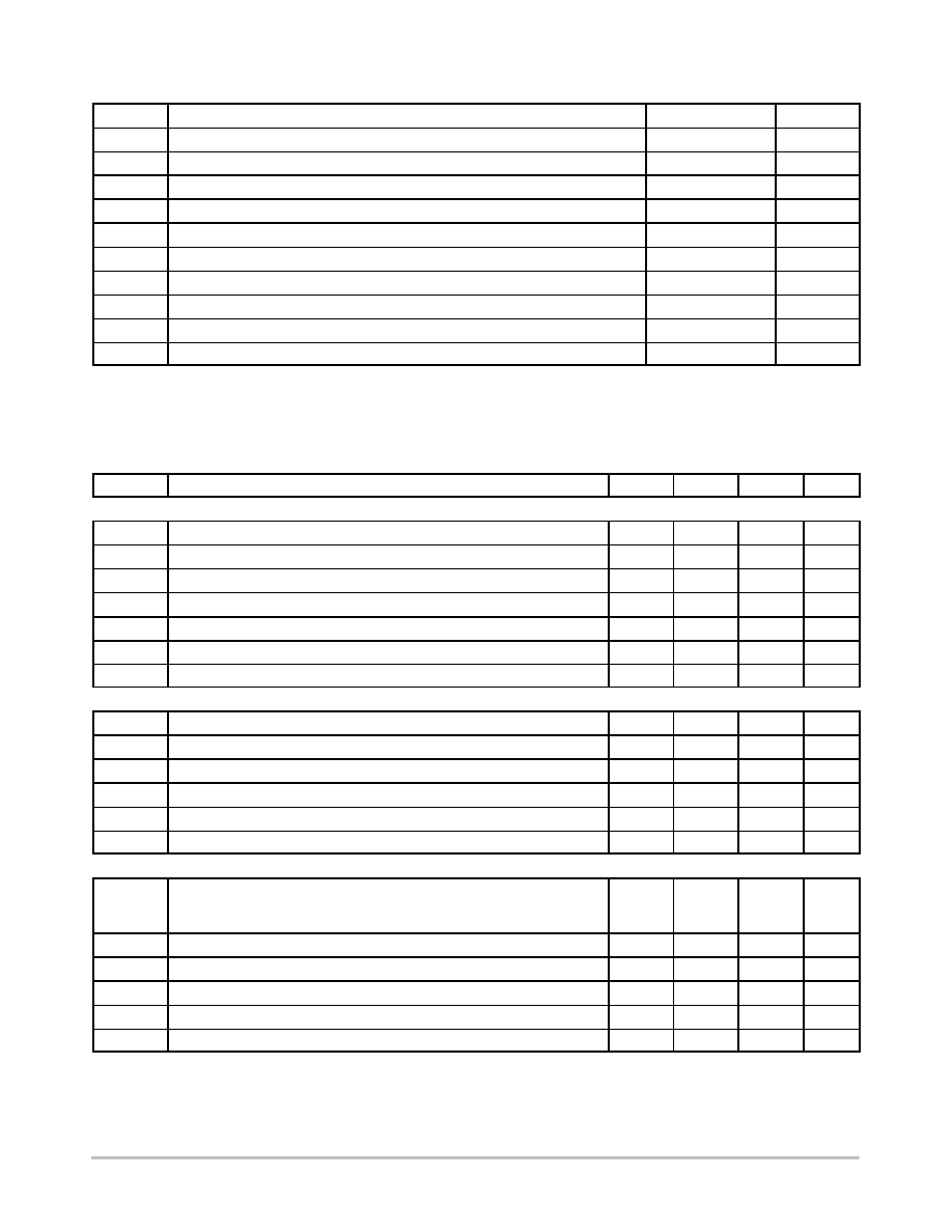
ELECTRICAL CHARACTERISTICS
(V
DD
= 10 V, V
BST
= 25 V, T
J
from -25
∞
C to +125
∞
C, unless otherwise specified.)
Symbol
Characteristic
Min
Typ
Max
Unit
High-Side Output Stage
V
HS_H
High-Side Output Voltage in High State @ Isource = -100 mA
22.5
23.5
-
V
V
HS_L
High-Side Output Voltage in Low State @ Isink = 100 mA
-
0.9
1.5
V
I
source_HS
Current Capability of the High-Side Drive Output in High State
-
0.5
-
A
I
sink_HS
Current Capability of the High-Side Drive Output in Low State
-
0.75
-
A
t
r-HS
High-Side Output Voltage Rise Time from 0.5 V to 12 V (C
L
= 1.0 nF)
-
25
-
ns
t
f-HS
High-Side Output Voltage Fall Time from 20 V to 0.5 V (C
L
= 1.0 nF)
-
25
-
ns
T
LS-HS
Delay from Low-Side Gate Drive Low (High) to High-Side Drive High (Low)
-
100
-
ns
Low-Side Output Stage
V
LS_H
Low-Side Output Voltage in High State @ Isource = -500 mA
7.4
8.2
-
V
V
LS_L
Low-Side Output Voltage in Low State @ Isink = 750 mA
-
1.3
1.7
V
I
source_LS
Current Capability of the Low-Side Drive Output in High State
-
0.5
-
A
I
sink_LS
Current Capability of the Low-Side Drive Output in Low State
-
0.75
-
A
t
r-LS
Low-Side Output Voltage Rise Time from 0.5 V to 7.0 V (C
L
= 2.0 nF)
-
25
-
ns
t
f-LS
Low-Side Output Voltage Fall Time from 9.5 V to 0.5 V (C
L
= 2.0 nF)
-
25
-
ns
Ramp Control
I
charge
C_ramp Current
@ Ipin5 = 100
m
A
@ Ipin5 = 1.5 mA
90
1400
102
1590
110
1800
m
A
Vcl
Pin5 Clamp Voltage @ Ipin5 = 1.5 mA
0.7
1.4
2.1
V
Vref
L
Ramp Control Reference Voltage, Vpin4 Falling
1.3
1. 5
1.7
V
Vref
H
Ramp Control Reference Voltage, Vpin4 Rising
2.25
2.5
2.75
V
V
rampHL
Ramp Voltage Maximum Value @ Ipin5 = 1.5 mA
3.2
3.6
4.2
V
V
rampLL
Ramp Voltage Low Voltage @ Ipin5 = 1.5 mA
-
-
100
mV

NCP4330
http://onsemi.com
4
ELECTRICAL CHARACTERISTICS (continued)
(V
DD
= 10 V, V
BST
= 25 V, T
J
from -25
∞
C to +125
∞
C, unless otherwise
specified.)
Symbol
Characteristic
Min
Typ
Max
Unit
V
DD
Management
UVD
H
Undervoltage Lockout Threshold (V
DD
Rising)
5.2
5.8
6.4
V
UVD
L
Undervoltage Lockout Threshold (V
DD
Falling)
4.9
5.2
5.5
V
H
UVD
Undervoltage Lockout Hysteresis
400
600
-
mV
I
DD1
I
DD2
I
DD3
Consumption:
@ Vpin4 = 3.0 V and Ipin5 = 500
m
A
@ Vpin4 = 0 V and Ipin5 = 500
m
A
@ Vpin4 Oscillating 0 to 3.0 V at 200 kHz, Ipin5 = 500
m
A
-
-
-
13
7.0
10
20
12
15
mA
Reset Block
V
rst_th
Reset Block Threshold
2.2
2.5
2.8
V
H
rst
Reset Comparator Hysteresis
0.8
1.0
-
V
T
reset
Reset Pulse Duration
-
250
500
ns
I
reset
C_ramp Pin Average Current, a 200 kHz, 50% duty cycle Pulse Generator
being applied to reset pin and 1.0 V to pin 4 (C_ramp) and @ Iramp = 0
0.3
0.7
-
mA
V
cl-neg
Negative Clamp Level @ Ipin3 = -2.0 mA
-0.5
-0.3
0
V
Temperature Protection
T
limit
Thermal Shutdown Threshold
-
150
-
∞
C
H
temp
Thermal Shutdown Hysteresis
-
50
-
∞
C

NCP4330
http://onsemi.com
5
-25
18
25
I
DD1
(mA)
8
Figure 3. I
DD1
Consumption
vs. Temperature
Figure 4. I
DD2
Consumption
vs. Temperature
Figure 5. I
DD3
Consumption
vs. Temperature
Figure 6. Undervoltage Lockout Upper
Threshold vs. Temperature
Figure 7. Undervoltage Lockout Lower
Threshold vs. Temperature
TEMPERATURE (
∞
C)
10
14
16
125
Figure 8. Undervoltage Lockout Hysteresis
vs. Temperature
12
-25
9.0
25
I
DD2
(mA)
5.0
TEMPERATURE (
∞
C)
5.8
7.4
8.2
125
6.6
-25
14
25
I
DD3
(mA)
8
TEMPERATURE (
∞
C)
10
12
13
125
11
-25
6.0
25
UVD_H (V)
5.5
TEMPERATURE (
∞
C)
5.6
5.8
5.9
125
5.7
9
-25
700
25
H_UVD (V)
460
TEMPERATURE (
∞
C)
500
580
620
125
540
-25
25
UVD_L (V)
5.14
TEMPERATURE (
∞
C)
5.16
5.20
5.22
125
5.18
660