
©
Semiconductor Components Industries, LLC, 2004
February, 2004 - Rev. 4
1
Publication Order Number:
NCP4672/D
NCP4672
Dual Linear Voltage
Regulators with V
in
and V
out
Voltage Detector
The NCP4672 is a dual linear voltage regulator with input voltage
and output voltage detectors. This part is useful in systems where
multiple voltages are required such as for core and I/O. The NCP4672
is very accurate at 2% over full input voltage and full load current. The
NCP4672 eliminates the need for external voltage supervision due to
the two built in voltage detectors. The voltage detector on the input is
set to 7.0 V. The output voltage detector is for channel 1 and is set to
2.9 V. An external capacitor is used to set the duration of this reset
signal. Other features include short circuit protection and thermal
shutdown protection. The NCP4672 has been designed to work with a
4.7
mF output capacitor having an ESR between 0.1 W and 5.0 W.
Features
∑
Accuracy: 2% at Full Voltage and Load
∑
Excellent Ripple Rejection: 70 dB @ 1 kHz
∑
Voltage Detector for Input Voltage
∑
Voltage Detector for Output Voltage
∑
Programmable Delay of Reset Signal
∑
Thermal Short Circuit Protection
∑
This is a Pb-Free Device
Typical Application
∑
Small Core and I/O Power
∑
Consumer Equipment
∑
Measurement Equipment
∑
Industrial Equipment
PIN CONFIGURATION
1
V
in
Rst
8 V
out1
2
V
out
Rst
3
C
D
4
V
in
7 GND1
6 GND2
5 V
out2
(Top View)
SOIC-8
NB SUFFIX
CASE 751
1
8
http://onsemi.com
Device
Package
Shipping
ORDERING INFORMATION
NCP4672DR2G
SOIC-8
(Pb-Free)
2500 Tape & Reel
MARKING
DIAGRAM
4672G
ALYW
1
8
4672G = Specific Device Code
A
= Assembly Location
L
= Wafer Lot
YW
= Date Code
For information on tape and reel specifications,
including part orientation and tape sizes, please
refer to our Tape and Reel Packaging Specifications
Brochure, BRD8011/D.
V
in
Rst
V
out
Rst
C
D
V
in
V
out1
GND1
GND2
V
out2
V
in
RST
10 nF
10 K
W
V
in
V
in
V
out1
V
out2
C
out2
4.7
m
F
C
out2
4.7
m
F
C
in
0.1
m
F
Figure 1. Typical Application Circuit

NCP4672
http://onsemi.com
2
MAXIMUM RATINGS
Rating
Symbol
Value
Unit
Input Voltage
V
inmax
-0.3 ~ 18
V
Output Voltage
V
out
-0.3 to V
in
+ 0.3
V
Output Current 1
Output Current 2
I
out1max
I
out2max
30
80
mA
mA
Output Short Circuit Duration
-
Infinite
-
Power Dissipation and Thermal Characteristics - SOIC-8
Power Dissipation
Thermal Resistance, Junction-to-Ambient
Minimum Pad Size
200 mm
2
Pad Size (Note 1)
Thermal Resistance, Junction-to-Case
P
D
R
q
JA
R
q
JC
Internally Limited
190
160
25
W
∞
C/W
∞
C/W
∞
C/W
Operating Junction Temperature Range
T
stg
-40 to 125
∞
C
Storage Temperature Range
T
solder
-55 to 150
∞
C
1. Refer to Figure 4 for more information.
PIN DESCRIPTION
Pin
Number
Symbol
Description
1
V
in RST
Open-collector, active-low output of the input voltage detector with hysteresis. Threshold levels are
typical 7.0 V/ 7.35 V at V
CC
pin.
2
V
o RST
Active-low output of the reset generator. Reset generator is based on sensing of the V
out1
voltage.
Sensing is with hysteresis - threshold levels are typically 2.9 V/ 2.95 V at V
out1
. Reset is generated at
rising edge of the V
out1
and it's duration is set by external capacitor connected to C
D
pin.
3
C
D
Programmable delay of the reset generator. Delay is adjusted by inserting a capacitor between C
D
and
GND (typically 10 ms for 10 nF capacitor).
4
V
CC
Supply Voltage
5
V
out2
1.8 V/ 80 mA LDO Regulator Output
6
GND2
Ground for V
out2
(internally connected with GND1)
7
GND1
Ground for V
out1
(internally connected with GND2)
8
V
out1
3.5 V/30 mA LDO Regulator Output
Recommended Conditions
(T
A
= 25
∞
C, C
in
= 0.1
m
F Ceramic, C
out
= 4.7
m
F)
Characteristics
Symbol
Min
Typ
Max
Unit
Input Voltage
V
in
3.8
12
16
V
Output Current (where V
out
remains within accuracy)
I
out1
I
out2
0
0
-
-
20
70
mA

NCP4672
http://onsemi.com
3
-
+
-
+
Thermal
Shutdown
-
+
V
ref
V
ref
V
ref
-
+
V
ref
-
+
V
ref
V
in
V
In RST
V
out1
V
o RST
C
D
V
out2
GND1
GND2
7.0 V
2.9 V
Figure 1.
Thermal
Shutdown
NCP4672
http://onsemi.com
4
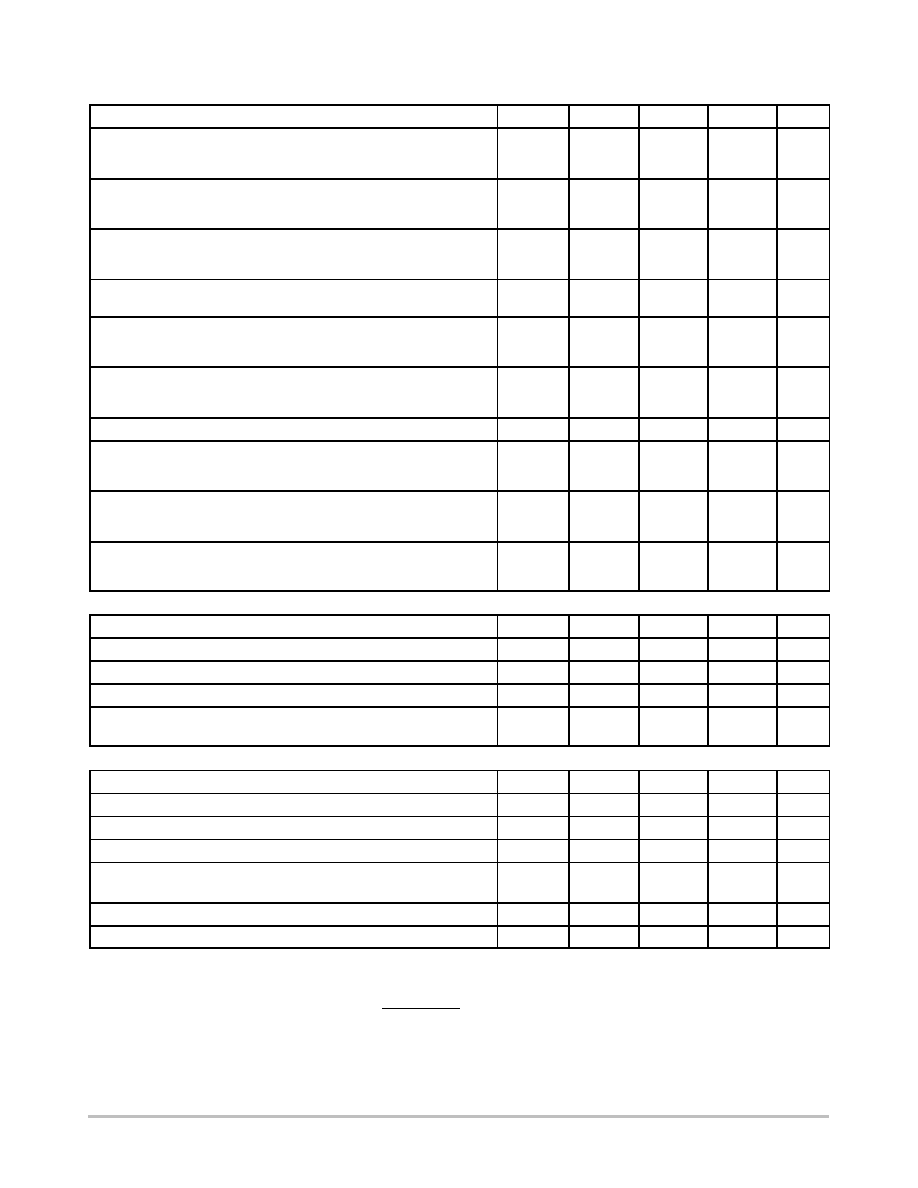
ELECTRICAL CHARACTERISTICS
(C
in
= 0.1
m
F Ceramic, C
out
= 4.7
m
F with ESR = 0.1 - 5.0
W
, V
in
= 12 V, T
A
= 25
∞
C)
Characteristics
Symbol
Min
Typ
Max
Unit
Output Voltage
V
out1
(V
in
= 4.5 V, I
out1
= 20 mA)
V
out2
(V
in
= 4.5 V, I
out2
= 40 mA)
V
adj
3.43
1.764
3.5
1.8
3.57
1.836
V
Line Regulation
V
out1
(V
in
= 4.5 V , I
out1
= 20 mA)
V
out2
(V
in
= 4.5 V to 10 V, I
out2
= 40 mA)
Reg
line
-
-
3.0
3.0
30
30
mV
Load Regulation
V
out1
(V
in
= 4.5 V, I
out1
= 0.1 mA to 20 mA)
V
out2
(V
in
= 4.5 V, I
out2
= 0.1 mA to 70 mA)
Reg
load
-
-
3.0
2.0
40
40
mV
Dropout Voltage
V
out1
(V
in
= 3.3 V, I
out1
= 20 mA)
V
in
- V
out1
-
150
300
mV
Ground Pin Current
(V
in
= 8.0 V, I
out1
= I
out2
= 0 mA)
(V
in
= 2.7 V, I
out1
= I
out2
= 0 mA, Rpu = infinite)
I
GND
-
-
1.0
3.0
2.0
-
mA
Short Current Limit
V
out1
V
out2
I
SC
30
80
60
150
-
-
mA
Thermal Shutdown
-
165
-
∞
C
Temperature Coefficient
V
out1
(T
J
= -30 to 85
∞
C, V
in
= 4.5 V, I
out1
= 20 mA)
V
out2
(T
J
= -30 to 85
∞
C, V
in
= 4.5 V, I
out2
= 40 mA)
T
C
-
-
100
100
-
-
ppm/
∞
C
Ripple Rejection (Note 6)
V
out1
(V
in
= 4.5 V, V
ripple
= 1.0 V, I
out1
= 20 mA, 120 Hz)
V
out2
(V
in
= 4.5 V, V
ripple
= 1.0 V, I
out2
= 40 mA, 120 Hz)
R
R
-
-
65
70
-
-
dB
Output Noise Voltage
V
out1
(V
in
= 4.5 V, f = 20 Hz - 80 kHz, I
out1
= 20 mA)
V
out2
(V
in
= 4.5 V, f = 20 Hz - 80 kHz, I
out2
= 40 mA)
V
n
-
-
80
50
-
-
m
V
rms
V
in
Detect
Detecting Voltage L (V
in
= H to L)
V
SLin
6.72
7.0
7.28
V
Detecting Voltage H (V
in
= L to H)
V
SHin
-
7.35
-
V
Hysteresis Voltage (V
in
= H to L to H)
D
V
Sin
140
350
560
mV
V
SLin
Temperature Coefficient (T
J
= -30
∞
C to +85
∞
C)
V
Slin
T
C
-
100
-
ppm/
∞
C
Low-Level Output Voltage (V
in
= 6.0 V, Vt1 = 5.0 V, Rt1 = 10 k
W
) (Note 5)
Threshold Operating Voltage (V
OPLin
= Vt1 = 1.0 V)
V
OLin1
V
OLin2
-
-
100
-
200
0.4
mV
V
V
out
Detect
Detecting Voltage L (V
in
= H to L)
V
SLout
2.78
2.9
3.020
V
Detecting Voltage H (V
in
= L to H)
V
SHout
-
2.95
-
V
Hysteresis Voltage (V
in
= H to L to H)
D
V
Sout
25
50
100
mV
V
SLin
Temperature Coefficient (T
J
= -30
∞
C to +85
∞
C)
V
SLin
T
C
-
100
-
ppm/
∞
C
Low-Level Output Voltage (V
out1
= 2.6 V)
V
OLout1
-
100
200
mV
o
e e Ou u
o age (
out1
6
)
Threshold Operating Voltage (V
OPLout
= 0.85 V)
OLout1
V
OLout2
-
00
-
00
0.4
V
Reset Delay Time (C
D
= 10 nF)
t
PLH
5
10
15
ms
"L" Transmission Delay Time (C
D
= 10 nF)
t
PHL
-
30
90
m
s
2. This device series contains ESD protection and exceeds the following tests:
Human Body Model 2000 V per MIL-STD-883, Method 3015
Machine Model Method 200 V.
3. The maximum package power dissipation is: PD
+
TJ(max)
*
TA
R
q
JA
4. Low duty cycle pulse techniques are used during testing to maintain the junction temperature as close to ambient as possible.
5. Refer to Figure 3.
6. Guaranteed by design.

NCP4672
http://onsemi.com
5
Figure 2. Dual Regulator Timing
Vi
(Pin4)
V
in RST
(Pin1)
V
out1
(Pin8)
V
o RST
(Pin2)
V
OPLout
*
V
SHout
D
V
Sout
V
SLout
V
OPLout
*
t
PLH
t
PHL
t
PLH
D
V
Sin
V
SHin
V
OPLin
*
V
OPLin
*
V
SLin
*; V
OPLin
shows theoretical on this chart.
V
OPLin
spec. must be specified on Pin 1 voltage (0.4 V)
*; V
OPLout
shows theoretical on this chart.
V
OPLout
spec. must be specified on Pin 2 voltage (0.4 V)
Figure 3. Threshold Operating Voltage V
OPLin
Under Condition V
OLin
= 0.4 V
-
+
-
+
1
4
7
10 k
W
Vt1
V
OPLin
= 1.0 V
typ
V
in RST
V
in
GND1
7.0 V
V
OLin
= 0.4 V
V
typ
= 5.0 V
V
max
= 16 V