Äîêóìåíòàöèÿ è îïèñàíèÿ www.docs.chipfind.ru
©
Semiconductor Components Industries, LLC, 2004
July, 2004 - Rev. 8
1
Publication Order Number:
NCP565/D
NCP565
1.5 A Low Dropout
Linear Regulator
The NCP565 low dropout linear regulator will provide 1.5 A at a
fixed output voltage or an adjustable voltage down to 0.9 V. The fast
loop response and low dropout voltage make this regulator ideal for
applications where low voltage and good load transient response are
important. Device protection includes current limit, short circuit
protection, and thermal shutdown. The NCP565 is packaged in a 5 pin
D
2
PAK for adjustable voltage version and a 3 pin D
2
PAK for fixed
voltage version.
Features
·
Pb-Free Packages are Available
·
Ultra Fast Transient Response (
t1.0 ms)
·
Low Ground Current (1.1 mA @ Iload = 1.5 A)
·
Low Dropout Voltage (0.9 V @ Iload = 1.5 A)
·
Low Noise (28
mVrms)
·
0.9 V Reference Voltage
·
Adjustable Output Voltage from 7.7 V down to 0.9 V
·
1.2 V Fixed Output Version. Other Fixed Voltages Available on
Request
·
Current Limit Protection (3.5 A)
·
Thermal Shutdown Protection (155
°
C)
Typical Applications
·
Servers
·
ASIC Power Supplies
·
Post Regulation for Power Supplies
·
Constant Current Source
http://onsemi.com
D
2
PAK
CASE 936A
ADJUSTABLE
1
5
Tab = Ground
Pin 1. N.C.
2. V
in
3. Ground
4. V
out
5. Adj
xx
= R4 or 12
A
= Assembly Location
WL = Wafer Lot
Y
= Year
WW = Work Week
G
= Pb-Free
See detailed ordering and shipping information in the package
dimensions section on page 3 of this data sheet.
ORDERING INFORMATION
1
2
3
D
2
PAK
CASE 936
FIXED
MARKING
DIAGRAMS
Tab = Ground
Pin 1. V
in
2. Ground
3. V
out
NC
P565D2Txx
AWLYWWG
NC
P565D2Txx
AWLYWWG
NCP565
http://onsemi.com
2
PIN DESCRIPTION
Pin No.
Adjustable Version
Pin No.
Fixed Version
Symbol
Description
ÁÁÁÁÁÁÁ
ÁÁÁÁÁÁÁ
1
ÁÁÁÁÁÁ
ÁÁÁÁÁÁ
-
ÁÁÁÁÁÁ
ÁÁÁÁÁÁ
N.C.
ÁÁÁÁÁÁÁÁÁÁÁÁÁÁÁÁÁ
ÁÁÁÁÁÁÁÁÁÁÁÁÁÁÁÁÁ
-
ÁÁÁÁÁÁÁ
ÁÁÁÁÁÁÁ
2
ÁÁÁÁÁÁ
ÁÁÁÁÁÁ
1
ÁÁÁÁÁÁ
ÁÁÁÁÁÁ
V
in
ÁÁÁÁÁÁÁÁÁÁÁÁÁÁÁÁÁ
ÁÁÁÁÁÁÁÁÁÁÁÁÁÁÁÁÁ
Positive Power Supply Input Voltage
ÁÁÁÁÁÁÁ
ÁÁÁÁÁÁÁ
3, Tab
ÁÁÁÁÁÁ
ÁÁÁÁÁÁ
2, Tab
ÁÁÁÁÁÁ
ÁÁÁÁÁÁ
Ground
ÁÁÁÁÁÁÁÁÁÁÁÁÁÁÁÁÁ
ÁÁÁÁÁÁÁÁÁÁÁÁÁÁÁÁÁ
Power Supply Ground
ÁÁÁÁÁÁÁ
ÁÁÁÁÁÁÁ
4
ÁÁÁÁÁÁ
ÁÁÁÁÁÁ
3
ÁÁÁÁÁÁ
ÁÁÁÁÁÁ
V
out
ÁÁÁÁÁÁÁÁÁÁÁÁÁÁÁÁÁ
ÁÁÁÁÁÁÁÁÁÁÁÁÁÁÁÁÁ
Regulated Output Voltage
ÁÁÁÁÁÁÁ
Á
ÁÁÁÁÁ
Á
ÁÁÁÁÁÁÁ
5
ÁÁÁÁÁÁ
Á
ÁÁÁÁ
Á
ÁÁÁÁÁÁ
-
ÁÁÁÁÁÁ
Á
ÁÁÁÁ
Á
ÁÁÁÁÁÁ
Adj
ÁÁÁÁÁÁÁÁÁÁÁÁÁÁÁÁÁ
Á
ÁÁÁÁÁÁÁÁÁÁÁÁÁÁÁ
Á
ÁÁÁÁÁÁÁÁÁÁÁÁÁÁÁÁÁ
This pin is to be connected to the R
sense
resistors on the output. The
linear regulator will attempt to maintain 0.9 V between this pin and
ground. Refer to Figure 1 for the equation.
MAXIMUM RATINGS
Rating
Symbol
Value
Unit
Input Voltage (Note 1)
V
in
9.0
V
Output Pin Voltage
V
out
-0.3 to V
in
+ 0.3
V
Adjust Pin Voltage
V
adj
-0.3 to V
in
+ 0.3
V
Thermal Characteristics (Note 2)
Case 936A
Thermal Resistance, Junction-to-Air
Thermal Resistance, Junction-to-Case
R
q
JA
R
q
JC
45
5.0
°
C/W
Operating Junction Temperature Range
T
J
-40 to 150
°
C
Storage Temperature Range
T
stg
-55 to 150
°
C
Maximum ratings are those values beyond which device damage can occur. Maximum ratings applied to the device are individual stress limit
values (not normal operating conditions) and are not valid simultaneously. If these limits are exceeded, device functional operation is not implied,
damage may occur and reliability may be affected.
1. This device series contains ESD protection and exceeds the following tests:
Human Body Model JESD 22-A114-B
Machine Model JESD 22-A115-A
2. The maximum package power dissipation is:
PD
+
TJ(max)
*
TA
R
q
JA
Figure 1. Typical Schematic, Adjustable Output
Voltage
Reference
Block
V
ref
= 0.9 V
Output
Stage
C1
R1
R2
C2
V
out
ADJ
GND
R1
+
R2
Vout
Vref
*
1
V
in
5.6
pF
GND
Figure 2. Typical Schematic, Fixed Output
Voltage
Reference
Block
V
ref
= 0.9 V
Output
Stage
C1
C2
V
out
GND
V
in
R1
R2
NCP565
http://onsemi.com
3
ELECTRICAL CHARACTERISTICS
(V
in
- V
out
= 1.6 V, V
out
= 0.9 V, T
J
= 25
°
C, C
in
= C
out
= 150
m
F, values unless otherwise noted.)
Characteristic
Symbol
Min
Typ
Max
Unit
ADJUSTABLE OUTPUT VERSION
Reference Voltage (10 mA < I
out
< 1.5 A; 2.5 V < V
in
< 9.0 V; T
J
= -10 to 105
°
C)
V
ref
0.882
(-2%)
0.9
0.918
(+2%)
V
Reference Voltage (10 mA < I
out
< 1.5 A; 2.5 V < V
in
< 9.0 V; T
J
= -40 to 125
°
C)
V
out
0.873
(-3%)
0.9
0.927
(+3%)
V
ADJ Pin Current
I
Adj
-
30
-
nA
Line Regulation (I
out
= 10 mA)
Reg
line
-
0.03
-
%
Load Regulation (10 mA < I
out
< 1.5 A)
Reg
load
-
0.03
-
%
Dropout Voltage (I
out
= 1.5 A) (Note 3)
Vdo
-
0.9
1.3
V
Current Limit
I
lim
1.6
3.5
-
A
Ripple Rejection (120 Hz; I
out
= 1.5 A)
RR
-
85
-
dB
Ripple Rejection (1 kHz; I
out
= 1.5 A)
RR
-
75
-
dB
Thermal Shutdown
-
150
-
°
C
Ground Current (I
out
= 1.5 A)
Iq
-
1.1
3.0
mA
Output Noise Voltage (f = 100 Hz to 100 kHz, I
out
= 1.5 A)
V
n
-
28
-
m
Vrms
FIXED OUTPUT VOLTAGE
Output Voltage (10 mA < I
out
< 1.5 A; 2.5 V < V
in
< 9.0 V; T
J
= -10 to 105
°
C)
V
out
1.176
(-2%)
1.2
1.224
(+2%)
%
Output Voltage (10 mA < I
out
< 1.5 A; 2.5 V < V
in
< 9.0 V; T
J
= -40 to 125
°
C)
V
out
1.164
(-3%)
1.2
1.236
(+3%)
%
Line Regulation (I
out
= 10 mA)
Reg
line
-
0.03
-
%
Load Regulation (10 mA < I
out
< 1.5 A)
Reg
load
-
0.03
-
%
Dropout Voltage (I
out
= 1.5 A) (Note 3)
Vdo
-
0.9
1.3
V
Current Limit
I
lim
1.6
3.5
-
A
Ripple Rejection (120 Hz; I
out
= 1.5 A)
RR
-
85
-
dB
Ripple Rejection (1 kHz; I
out
= 1.5 A)
RR
-
75
-
dB
Thermal Shutdown
-
150
-
°
C
Ground Current (I
out
= 1.5 A)
Iq
-
1.1
3.0
mA
Output Noise Voltage (f = 100 Hz to 100 kHz, I
out
= 1.5 A)
V
n
-
28
-
m
Vrms
3. Dropout voltage is a measurement of the minimum input/output differential at full load.
ORDERING INFORMATION
Device
Nominal Output Voltage*
Package
Shipping
NCP565D2T
Adj
D
2
PAK
50 Tube
NCP565D2TR4
Adj
D
2
PAK
800 Tape & Reel
NCP565D2TR4G
Adj
D
2
PAK
(Pb-Free)
800 Tape & Reel
NCP565D2T12
Fixed
D
2
PAK
50 Tube
NCP565D2T12R4
Fixed
D
2
PAK
800 Tape & Reel
NCP565D2T12R4G
Fixed
D
2
PAK
(Pb-Free)
800 Tape & Reel
*For other fixed output versions, please contact the factory.
For information on tape and reel specifications, including part orientation and tape sizes, please refer to our Tape and Reel Packaging
Specifications Brochure, BRD8011/D.
NCP565
http://onsemi.com
4
TYPICAL CHARACTERISTICS
Figure 3. Output Voltage vs. Temperature
0.9005
0.9000
0.8995
0.8990
0.8985
0.8980
0.8975
0.8970
-50
0
50
100
150
T
J
, JUNCTION TEMPERATURE (
°
C)
V
ref
, REFERENCE VOL
T
AGE (V)
Figure 4. Short Circuit Current Limit
vs. Temperature
3.90
-50
0
50
100
150
T
J
, JUNCTION TEMPERATURE (
°
C)
I
SC
, SHOR
T CIRCUIT CURRENT LIMIT (A)
3.85
3.80
3.75
3.70
3.65
3.60
3.55
3.50
3.45
3.40
3.35
1.2
-50
0
50
100
150
T
J
, JUNCTION TEMPERATURE (
°
C)
V
in
- V
out
, DROPOUT VOL
T
AGE (V)
Figure 5. Dropout Voltage vs. Temperature
Figure 6. Ground Current vs. Temperature
1.0
0.8
0.6
0.4
0.2
0
I
out
= 1.5 A
I
out
= 50 mA
1.16
-50
0
50
100
150
T
J
, JUNCTION TEMPERATURE (
°
C)
I
GND
, GROUND CURRENT (mA)
1.14
1.12
1.10
1.08
1.06
1.04
1.02
1.00
0.98
0.96
-25
25
75
125
-25
25
75
125
-25
25
75
125
-25
25
75
125
100
90
80
70
60
50
40
30
20
10
0
10
1000000
RIPPLE REJECTION (dB)
F, FREQUENCY (Hz)
100
1000
10000
100000
I
out
= 1.5 A
V
in
= 2.5 V
V
out
= 0.9 V
C
in
= C
out
= 150
m
F
V
in
= 2.5 V
V
out
= 0.9 V
C
in
= C
out
= 150
m
F
C
in
= C
out
= 150
m
F
V
in
= 2.5 V
V
out
= 0.9 V
I
out
= 1.5 V
C
in
= C
out
= 150
m
F
1.12
1.14
1.16
1.18
1.2
1.22
1.24
1.26
1.28
0
300
600
900
1200
1500
I
out
, OUTPUT CURRENT (mA)
I
GND
, GROUND CURRENT (mA)
Figure 7. Ground Current vs. Output Current
Figure 8. Ripple Rejection vs. Frequency
NCP565
http://onsemi.com
5
TYPICAL CHARACTERISTICS
50
40
30
20
10
0
1.50
1.00
0.50
0
0
50
150
200
250
300
350
400
TIME (nS)
I
out
, OUTPUT
CURRENT (A)
OUTPUT VOL
T
AGE
DEVIA
TION (mV)
10
0
-10
-20
-30
-40
1.50
1.00
0.50
0
0
50
100
150
200
250
300
350
400
TIME (nS)
I
out
, OUTPUT
CURRENT (A)
OUTPUT VOL
T
AGE
DEVIA
TION (mV)
Figure 9. Load Transient from 10 mA to 1.5 A
10
0
-10
-20
-30
-40
1.50
1.00
0.50
0
0
0.5
1.0
1.5
2.0
2.5
3.0
3.5
4.0
TIME (
m
s)
I
out
, OUTPUT
CURRENT (A)
OUTPUT VOL
T
AGE
DEVIA
TION (mV)
Figure 10. Load Transient from 10 mA to 1.5 A
Figure 11. Load Transient from 1.5 A to 10 mA
50
40
30
20
10
0
1.50
1.00
0.50
0
0
0.2
0.4
0.6
0.8
1.0
1.2
1.4
1.6
TIME (
m
s)
I
out
, OUTPUT
CURRENT (A)
OUTPUT VOL
T
AGE
DEVIA
TION (mV)
Figure 12. Load Transient from 1.5 A to 10 mA
100
90
80
70
60
50
40
30
20
10
0
Start 1.0 kHz
Stop 100 kHz
NOISE DENSITY (nV
rm
s
/
Hz
)
FREQUENCY (kHz)
Figure 13. Noise Density vs. Frequency
100
90
80
70
60
50
40
30
20
10
0
Start 1.0 kHz
Stop 100 kHz
FREQUENCY (kHz)
Figure 14. Noise Density vs. Frequency
V
in
= 4.59 V
V
out
= 0.9 V
V
in
= 4.59 V
V
out
= 0.9 V
V
in
= 4.59 V
V
out
= 0.9 V
V
in
= 4.59 V
V
out
= 0.9 V
V
in
= 3.0 V
V
out
= 0.9 V
I
out
= 10 mA
V
in
= 3.0 V
V
out
= 0.9 V
I
out
= 1.5 A
100
-50
NOISE DENSITY (nV
rm
s
/
Hz
)
NCP565
http://onsemi.com
6
APPLICATION INFORMATION
The NCP565 low dropout linear regulator provides
adjustable voltages at currents up to 1.5 A. It features ultra
fast transient response and low dropout voltage. These
devices contain output current limiting, short circuit
protection and thermal shutdown protection.
Input, Output Capacitor and Stability
An input bypass capacitor is recommended to improve
transient response or if the regulator is located more than a
few inches from the power source. This will reduce the
circuit's sensitivity to the input line impedance at high
frequencies and significantly enhance the output transient
response. Different types and different sizes of input
capacitors can be chosen dependent on the quality of power
supply. A 150
mF OSCON 16SA150M type from Sanyo
should be adequate for most applications. The bypass
capacitor should be mounted with shortest possible lead or
track length directly across the regulator's input terminals.
The output capacitor is required for stability. The NCP565
remains stable with ceramic, tantalum, and aluminum-
electrolytic capacitors with a minimum value of 1.0
mF as
long as the ESR remains between 50 m
W and 2.5 W. The
NCP565 is optimized for use with a 150
mF OSCON
16SA150M type in parallel with a 10
mF OSCON 10SL10M
type from Sanyo. The 10
mF capacitor is used for best AC
stability while 150
mF capacitor is used for achieving
excellent output transient response. The output capacitors
should be placed as close as possible to the output pin of the
device. If not, the excellent load transient response of
NCP565 will be degraded.
Adjustable Operation
The typical application circuit for the adjustable output
regulators is shown in Figure 1. The adjustable device
develops and maintains the nominal 0.9 V reference voltage
between Adj and ground pins. A resistor divider network R1
and R2 causes a fixed current to flow to ground. This current
creates a voltage across R1 that adds to the 0.9 V across R2
and sets the overall output voltage.
The output voltage is set according to the formula:
Vout
+
Vref
R1
)
R2
R2
*
IAdj
R2
The adjust pin current, Iadj, is typically 30 nA and
normally much lower than the current flowing through R1
and R2, thus it generates a small output voltage error that can
usually be ignored.
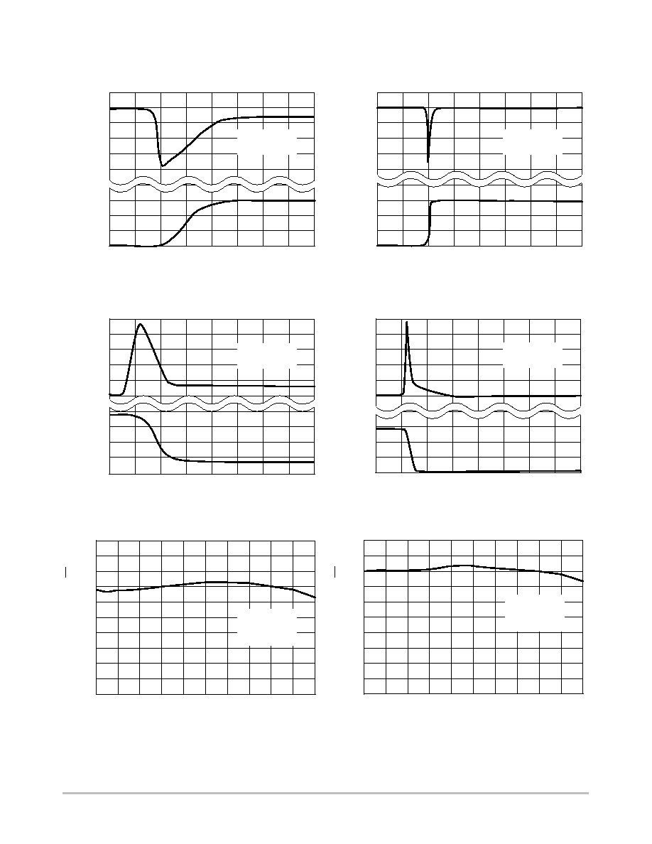
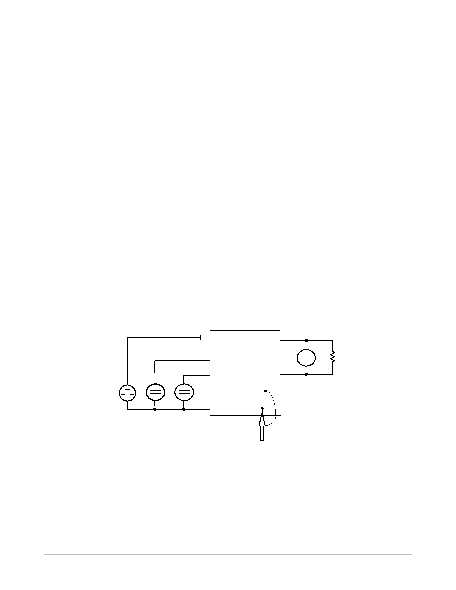
Load Transient Measurement
Large load current changes are always presented in
microprocessor applications. Therefore good load transient
performance is required for the power stage. NCP565 has
the feature of ultra fast transient response. Its load transient
responses in Figures 9 through 12 are tested on evaluation
board shown in Figure 15. On the evaluation board, it
consists of NCP565 regulator circuit with decoupling and
filter capacitors and the pulse controlled current sink to
obtain load current transitions. The load current transitions
are measured by current probe. Because the signal from
current probe has some time delay, it causes
un-synchronization between the load current transition and
output voltage response, which is shown in Figures 9
through 12.
NCP565
Evaluation Board
GEN
GND
V
RL
GND
Scope Voltage Probe
+
+
Pulse
Figure 15. Schematic for Transient Response Measurement
V
out
-V
CC
V
in
NCP565
http://onsemi.com
7
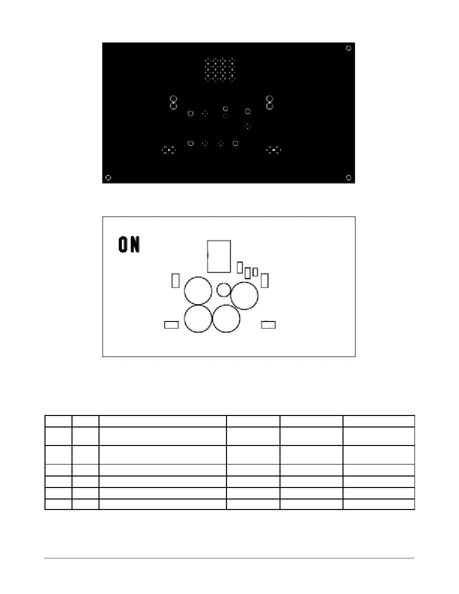
PCB Layout Considerations
Good PCB layout plays an important role in achieving
good load transient performance. Because it is very sensitive
to its PCB layout, particular care has to be taken when
tackling Printed Circuit Board (PCB) layout. The figures
below give an example of a layout where parasitic elements
are minimized. For microprocessor applications it is
customary to use an output capacitor network consisting of
several capacitors in parallel. This reduces the overall ESR
and reduces the instantaneous output voltage drop under
transient load conditions. The output capacitor network
should be as close as possible to the load for the best results.
The schematic of NCP565 typical application circuit, which
this PCB layout is base on, is shown in Figure 16. The output
voltage is set to 3.3 V for this demonstration board according
to the feedback resistors in the Table 1.
Figure 16. Schematic of NCP565 Typical Application Circuit
V
in
V
out
NCP565
GND
Adj
C
1
150
m
R
2
15.8 k
V
out
V
in
GND
C
2
150
m
NC
C
4
10
m
C
3
150
m
GND
C
3
150
m
C
6
5.6 p
R
1
42.2 k
2
1
3
5
4
Figure 17. Top Layer
NCP565
http://onsemi.com
8
Figure 18. Bottom Layer
Figure 19. Silkscreen Layer
D1
C1
C2
C3
C4
C5
C6
GND
R1
R2
GND
VIN
VOUT
NCP565
ON Semiconductor
www.onsemi.com
July, 2003
Table 1. Bill of Materials for NCP565 Adj Demonstration Board
Item
Used #
Component
Designators
Suppliers
Part Number
1
4
Radial Lead Aluminum Capacitor
150
m
F/16 V
C1, C2, C3, C5
Sanyo Oscon
16SA150M
2
1
Radial Lead Aluminum Capacitor
10
m
F/10 V
C4
Sanyo Oscon
10SL10M
3
1
SMT Chip Resistor (0805) 15.8 K 1%
R2
Vishay
CRCW08051582F
4
1
SMT Chip Resistor (0805) 42.2 K 1%
R1
Vishay
CRCW08054222F
5
1
SMT Ceramic Capacitor (0603) 5.6 pF 10%
C6
Vishay
VJ0603A5R6KXAA
6
1
NCP565 Low Dropout Linear Regulator
U1
ON Semiconductor
NCP565D2TR4
NCP565
http://onsemi.com
9
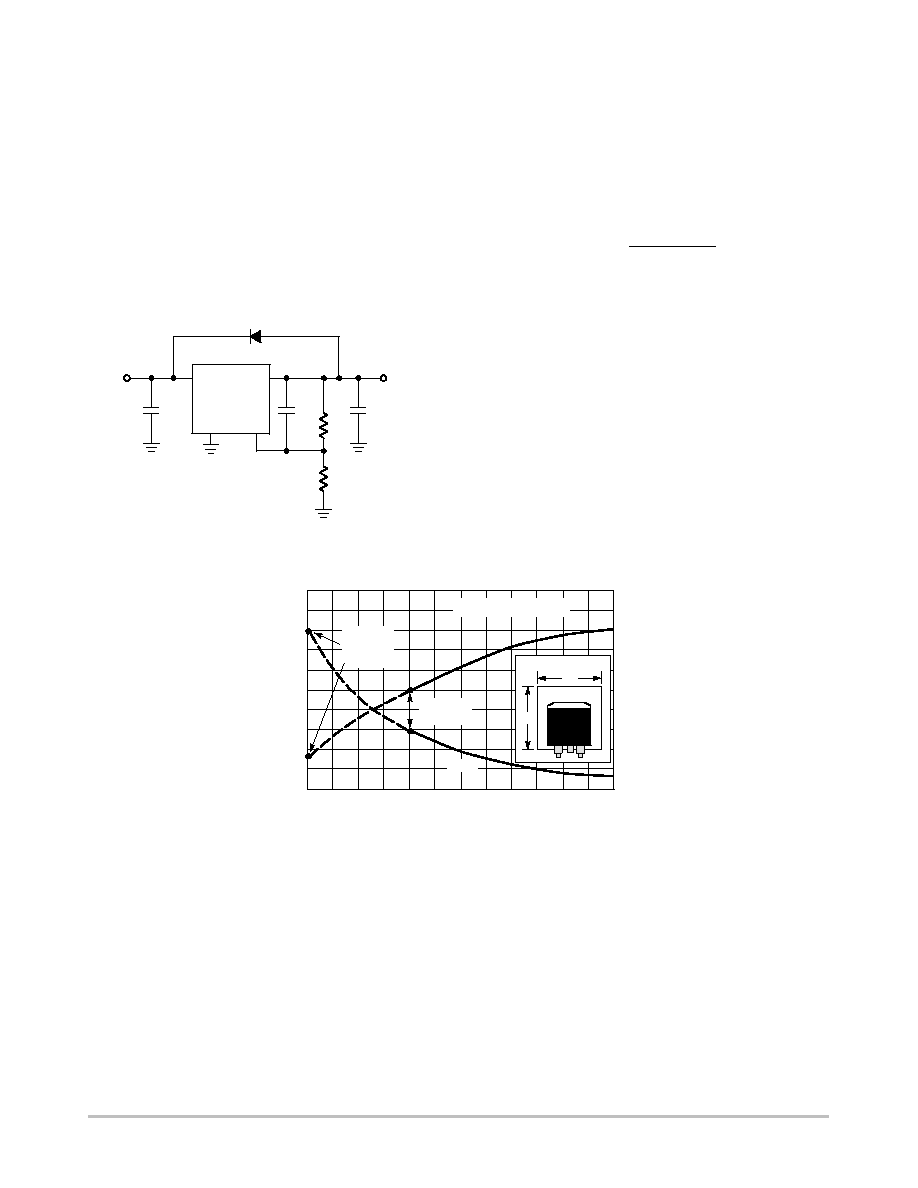
Protection Diodes
When large external capacitors are used with a linear
regulator it is sometimes necessary to add protection diodes.
If the input voltage of the regulator gets shorted, the output
capacitor will discharge into the output of the regulator. The
discharge current depends on the value of the capacitor, the
output voltage and the rate at which V
in
drops. In the
NCP565 linear regulator, the discharge path is through a
large junction and protection diodes are not usually needed.
If the regulator is used with large values of output
capacitance and the input voltage is instantaneously shorted
to ground, damage can occur. In this case, a diode connected
as shown in Figure 20 is recommended.
V
in
V
out
NCP565
GND
Adj
C
1
C
Adj
R
1
R
2
1N4002 (Optional)
C
2
V
out
Figure 20. Protection Diode for Large
Output Capacitors
V
in
Thermal Considerations
This series contains an internal thermal limiting circuit
that is designed to protect the regulator in the event that the
maximum junction temperature is exceeded. This feature
provides protection from a catastrophic device failure due to
accidental overheating. It is not intended to be used as a
substitute for proper heat sinking. The maximum device
power dissipation can be calculated by:
PD
+
TJ(max)
*
TA
R
q
JA
The devices are available in surface mount D
2
PAK
package. The package has an exposed metal tab that is
specifically designed to reduce the junction to air thermal
resistance, R
qJA
, by utilizing the printed circuit board
copper as a heat dissipater. Figure 21 shows typical R
qJA
values that can be obtained from a square pattern using
economical single sided 2.0 ounce copper board material.
The final product thermal limits should be tested and
quantified in order to insure acceptable performance and
reliability. The actual R
qJA
can vary considerably from the
graph shown. This will be due to any changes made in the
copper aspect ratio of the final layout, adjacent heat sources,
and air flow.
Figure 21. 3-Pin and 5-Pin D
2
PAK
Thermal Resistance and Maximum Power
Dissipation vs. P.C.B Length
R
,
THERMAL
RESIST
ANCE
JA
JUNCTION-T
O-AIR ( C/W)
°
ÎÎÎÎ
ÎÎÎÎ
ÎÎÎÎ
ÎÎÎÎ
P D
, MAXIMUM POWER DISSIP
A
TION (W)
30
40
50
60
70
80
Minimum
Size Pad
2.0 oz. Copper
L
L
Free Air
Mounted
Vertically
R
qJA
1.0
1.5
2.0
2.5
3.0
3.5
0
10
20
30
25
15
5.0
L, LENGTH OF COPPER (mm)
P
D(max)
for T
A
= +50
°
C
NCP565
http://onsemi.com
10
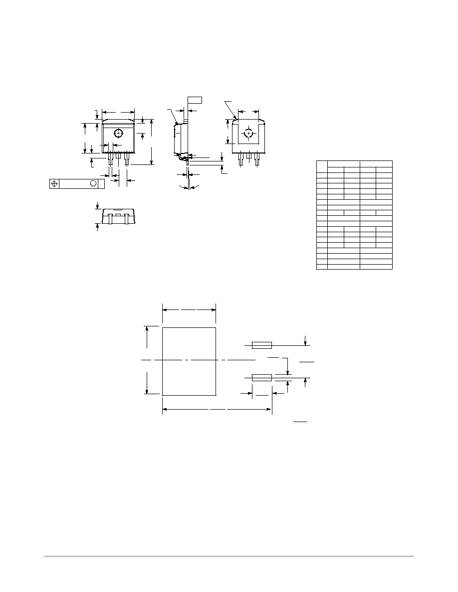
PACKAGE DIMENSIONS
D
2
PAK-3
D2T SUFFIX
CASE 936-03
ISSUE B
5 REF
5 REF
V
U
TERMINAL 4
NOTES:
1. DIMENSIONING AND TOLERANCING PER ANSI
Y14.5M, 1982.
2. CONTROLLING DIMENSION: INCH.
3. TAB CONTOUR OPTIONAL WITHIN DIMENSIONS
A AND K.
4. DIMENSIONS U AND V ESTABLISH A MINIMUM
MOUNTING SURFACE FOR TERMINAL 4.
5. DIMENSIONS A AND B DO NOT INCLUDE MOLD
FLASH OR GATE PROTRUSIONS. MOLD FLASH
AND GATE PROTRUSIONS NOT TO EXCEED
0.025 (0.635) MAXIMUM.
DIM
A
MIN
MAX
MIN
MAX
MILLIMETERS
0.386
0.403
9.804
10.236
INCHES
B
0.356
0.368
9.042
9.347
C
0.170
0.180
4.318
4.572
D
0.026
0.036
0.660
0.914
E
0.045
0.055
1.143
1.397
F
0.051 REF
1.295 REF
G
0.100 BSC
2.540 BSC
H
0.539
0.579 13.691
14.707
J
0.125 MAX
3.175 MAX
K
0.050 REF
1.270 REF
L
0.000
0.010
0.000
0.254
M
0.088
0.102
2.235
2.591
N
0.018
0.026
0.457
0.660
P
0.058
0.078
1.473
1.981
R
S
0.116 REF
2.946 REF
U
0.200 MIN
5.080 MIN
V
0.250 MIN
6.350 MIN
_
_
A
1 2
3
K
F
B
J
S
H
D
G
C
M
0.010 (0.254)
T
E
M
L
P
N
R
-T-
OPTIONAL
CHAMFER
8.38
0.33
1.016
0.04
17.02
0.67
10.66
0.42
3.05
0.12
5.08
0.20
mm
inches
SCALE 3:1
*For additional information on our Pb-Free strategy and soldering
details, please download the ON Semiconductor Soldering and
Mounting Techniques Reference Manual, SOLDERRM/D.
SOLDERING FOOTPRINT*
NCP565
http://onsemi.com
11
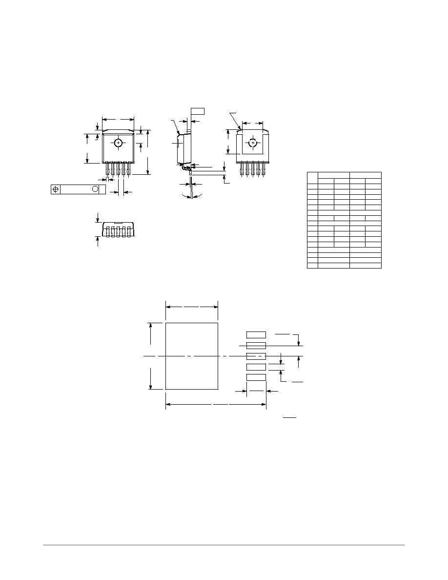
PACKAGE DIMENSIONS
D
2
PAK-5
D2T SUFFIX
CASE 936A-02
ISSUE B
5 REF
A
1 2 3
K
B
S
H
D
G
C
E
M
L
P
N
R
V
U
TERMINAL 6
NOTES:
1. DIMENSIONING AND TOLERANCING PER ANSI
Y14.5M, 1982.
2. CONTROLLING DIMENSION: INCH.
3. TAB CONTOUR OPTIONAL WITHIN DIMENSIONS A
AND K.
4. DIMENSIONS U AND V ESTABLISH A MINIMUM
MOUNTING SURFACE FOR TERMINAL 6.
5. DIMENSIONS A AND B DO NOT INCLUDE MOLD
FLASH OR GATE PROTRUSIONS. MOLD FLASH
AND GATE PROTRUSIONS NOT TO EXCEED 0.025
(0.635) MAXIMUM.
DIM
A
MIN
MAX
MIN
MAX
MILLIMETERS
0.386
0.403
9.804
10.236
INCHES
B
0.356
0.368
9.042
9.347
C
0.170
0.180
4.318
4.572
D
0.026
0.036
0.660
0.914
E
0.045
0.055
1.143
1.397
G
0.067 BSC
1.702 BSC
H
0.539
0.579 13.691
14.707
K
0.050 REF
1.270 REF
L
0.000
0.010
0.000
0.254
M
0.088
0.102
2.235
2.591
N
0.018
0.026
0.457
0.660
P
0.058
0.078
1.473
1.981
R
5 REF
S
0.116 REF
2.946 REF
U
0.200 MIN
5.080 MIN
V
0.250 MIN
6.350 MIN
_
_
4 5
M
0.010 (0.254)
T
-T-
OPTIONAL
CHAMFER
8.38
0.33
1.016
0.04
16.02
0.63
10.66
0.42
3.05
0.12
1.702
0.067
SCALE 3:1
mm
inches
*For additional information on our Pb-Free strategy and soldering
details, please download the ON Semiconductor Soldering and
Mounting Techniques Reference Manual, SOLDERRM/D.
SOLDERING FOOTPRINT*

NCP565
http://onsemi.com
12
ON Semiconductor and are registered trademarks of Semiconductor Components Industries, LLC (SCILLC). SCILLC reserves the right to make changes without further notice
to any products herein. SCILLC makes no warranty, representation or guarantee regarding the suitability of its products for any particular purpose, nor does SCILLC assume any liability
arising out of the application or use of any product or circuit, and specifically disclaims any and all liability, including without limitation special, consequential or incidental damages.
"Typical" parameters which may be provided in SCILLC data sheets and/or specifications can and do vary in different applications and actual performance may vary over time. All
operating parameters, including "Typicals" must be validated for each customer application by customer's technical experts. SCILLC does not convey any license under its patent rights
nor the rights of others. SCILLC products are not designed, intended, or authorized for use as components in systems intended for surgical implant into the body, or other applications
intended to support or sustain life, or for any other application in which the failure of the SCILLC product could create a situation where personal injury or death may occur. Should
Buyer purchase or use SCILLC products for any such unintended or unauthorized application, Buyer shall indemnify and hold SCILLC and its officers, employees, subsidiaries, affiliates,
and distributors harmless against all claims, costs, damages, and expenses, and reasonable attorney fees arising out of, directly or indirectly, any claim of personal injury or death
associated with such unintended or unauthorized use, even if such claim alleges that SCILLC was negligent regarding the design or manufacture of the part. SCILLC is an Equal
Opportunity/Affirmative Action Employer. This literature is subject to all applicable copyright laws and is not for resale in any manner.
PUBLICATION ORDERING INFORMATION
N. American Technical Support: 800-282-9855 Toll Free
USA/Canada
Japan: ON Semiconductor, Japan Customer Focus Center
2-9-1 Kamimeguro, Meguro-ku, Tokyo, Japan 153-0051
Phone: 81-3-5773-3850
NCP565/D
The product described herein (NCP565), may be covered by one or more of the following U.S. patents: 5,920,184; 5,834,926.
There may be other patents pending.
LITERATURE FULFILLMENT:
Literature Distribution Center for ON Semiconductor
P.O. Box 61312, Phoenix, Arizona 85082-1312 USA
Phone: 480-829-7710 or 800-344-3860 Toll Free USA/Canada
Fax: 480-829-7709 or 800-344-3867 Toll Free USA/Canada
Email: orderlit@onsemi.com
ON Semiconductor Website: http://onsemi.com
Order Literature: http://www.onsemi.com/litorder
For additional information, please contact your
local Sales Representative.