Äîêóìåíòàöèÿ è îïèñàíèÿ www.docs.chipfind.ru
© Semiconductor Components Industries, LLC, 2005
August, 2005 - Rev. 5
1
Publication Order Number:
NL17SZ07/D
NL17SZ07
Single Non-Inverting Buffer
with Open Drain Output
The NL17SZ07 is a high performance single inverter with open
drain outputs operating from a 1.65 to 5.5 V supply.
The Output stage is open drain with Over Voltage Tolerance. This
allows the NL17SZ07 to be used to interface 5.0 V circuits to circuits
of any voltage between 0 and +7.0 V.
·
Tiny SOT-353 and SOT-553 Packages
·
Extremely High Speed: t
PD
2.5 ns (typical) at V
CC
= 5 V
·
Designed for 1.65 V to 5.5 V V
CC
Operation, CMOS Compatible
·
Over Voltage Tolerant Inputs V
IN
may be Between 0 and 7.0 V for
V
CC
Between 0.5 and 5.4 V
·
TTL Compatible - Interface Capability with 5.0 V TTL Logic with
V
CC
= 2.7 V to 3.6 V
·
LVCMOS Compatible
·
24 mA Output Sink Capability, Pullup may be between 0 and 7.0 V
·
Near Zero Static Supply Current Substantially Reduces System
Power Requirements
·
Chip Complexity: FET = 20
·
Pb-Free Packages are Available
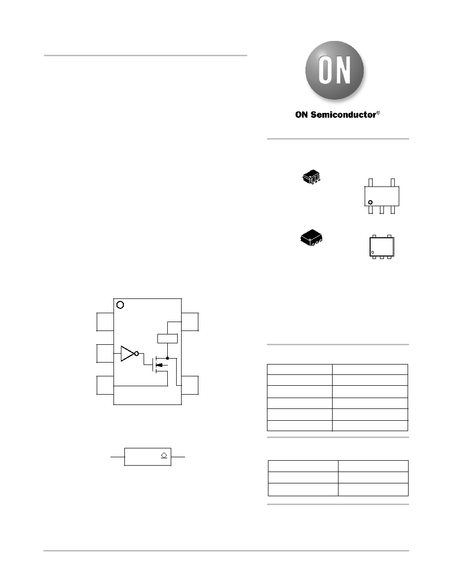
V
CC
NC
IN A
OUT Y
GND
IN A
OUT Y
1
OVT
Figure 1. Pinout
Figure 2. Logic Symbol
1
2
3
4
5
MARKING
DIAGRAM
http://onsemi.com
VX M G
G
SC-88A / SOT-353 / SC-70
DF SUFFIX
CASE 419A
M
= Date Code
A
= Assembly Location
Y
= Year
W
= Work Week
G
= Pb-Free Package
(Note: Microdot may be in either location)
PIN ASSIGNMENT
1
2
3
GND
NC
IN A
4
5
V
CC
OUT Y
Pin
Function
See detailed ordering and shipping information in the package
dimensions section on page 4 of this data sheet.
ORDERING INFORMATION
FUNCTION TABLE
L
A Input
Y Output
L
H
Z
SOT-553
XV5 SUFFIX
CASE 463B
L7 D G
G
NL17SZ07
http://onsemi.com
2
MAXIMUM RATINGS
Symbol
Characteristics
Value
Unit
V
CC
DC Supply Voltage
*0.5 to )7.0
V
V
I
DC Input Voltage
*0.5 V
I
)7.0
V
V
O
DC Output Voltage
Output in Z or LOW State (Note 1)
*0.5 V
O
7.0
V
I
IK
DC Input Diode Current
V
I
< GND
*50
mA
I
OK
DC Output Diode Current
V
O
< GND
*50
mA
I
O
DC Output Sink Current
$50
mA
I
CC
DC Supply Current per Supply Pin
$100
mA
I
GND
DC Ground Current per Ground Pin
$100
mA
T
STG
Storage Temperature Range
*65 to )150
°C
P
D
Power Dissipation in Still Air
SOT-353
SOT-553
186
135
mW
q
JA
Thermal Resistance
SOT-353
SOT-553
350
496
°C/W
T
L
Lead Temperature, 1 mm from Case for 10 Seconds
260
°C
T
J
Junction Temperature Under Bias
)150
°C
I
Latch-Up
Latch-Up Performance
Above V
CC
and Below GND at 85°C (Note 5)
$500
mA
MSL
Moisture Sensitivity
Level 1
F
R
Flammability Rating
Oxygen Index: 28 to 34
UL 94 V-0 @ 0.125 in
ESD
ESD Classification
Human Body Model (Note 3)
Machine Model (Note 4)
Charged Device Model (Note 5)
Class IC
Class A
N/A
Maximum ratings are those values beyond which device damage can occur. Maximum ratings applied to the device are individual stress limit
values (not normal operating conditions) and are not valid simultaneously. If these limits are exceeded, device functional operation is not implied,
damage may occur and reliability may be affected.
1. I
O
absolute maximum rating must be observed.
2. Tested to EIA/JESD22-A114-A, rated to EIA/JESD22-A114-B.
3. Tested to EIA/JESD22-A115-A, rated to EIA/JESD22-A115-A.
4. Tested to JESD22-C101-A.
5. Tested to EIA/JESD78.
RECOMMENDED OPERATING CONDITIONS
Symbol
Parameter
Min
Max
Unit
V
CC
Supply Voltage
Operating
Data Retention Only
1.65
1.5
5.5
5.5
V
V
I
Input Voltage
0
5.5
V
V
O
Output Voltage
(Z or LOW State)
0
5.5
V
T
A
Operating Free-Air Temperature
-55
)125
°C
t/V
Input Transition Rise or Fall Rate
V
CC
= 2.5 V $0.2 V
V
CC
= 3.0 V $0.3 V
V
CC
= 5.0 V $0.5 V
0
0
0
20
10
5
ns/V
NL17SZ07
http://onsemi.com
3
DC ELECTRICAL CHARACTERISTICS
Symbol
Parameter
Condition
V
CC
(V)
T
A
= 25°C
*55°C T
A
125°C
Unit
Min
Typ
Max
Min
Max
V
IH
High-Level Input Voltage
1.65 to 1.95
2.3 to 5.5
0.7 V
CC
0.7 V
CC
0.7 V
CC
0.7 V
CC
V
V
IL
Low-Level Input Voltage
1.65 to 1.95
2.3 to 5.5
0.3 V
CC
0.3 V
CC
0.3V
CC
0.3 V
CC
V
I
LKG
Z-State Output Leakage
Current
V
IN
= V
IH
V
OUT
= V
CC
or GND
2.3 to 5.5
$5.0
$10.0
mA
V
OL
Low-Level Output
Voltage
V
IN
= V
IL
I
OL
= 100 mA
1.65 to 5.5
0.0
0.1
0.1
V
I
OL
= 4 mA
1.65
0.08
0.24
0.24
I
OL
= 8 mA
2.3
0.20
0.3
0.3
I
OL
= 12 mA
2.7
0.22
0.4
0.4
I
OL
= 16 mA
3.0
0.28
0.4
0.4
I
OL
= 24 mA
3.0
0.38
0.55
0.55
I
OL
= 32 mA
4.5
0.42
0.55
0.55
I
IN
Input Leakage Current
V
IN
or V
OUT
= V
CC
or GND
0 to 5.5
$0.1
$1.0
mA
I
OFF
Power Off-Output
Leakage Current
V
OUT
= 5.5 V
0
1
10
mA
I
CC
Quiescent Supply Current
V
IN
= V
CC
or GND
5.5
1
10
mA
I
CCT
Quiescent Supply Current
V
IN
= 3.0 V
3.6
10
100
mA
ÎÎÎÎÎÎÎÎÎÎÎÎÎÎÎÎÎÎÎÎÎÎÎÎÎÎÎÎÎÎÎÎÎ
ÎÎÎÎÎÎÎÎÎÎÎÎÎÎÎÎÎÎÎÎÎÎÎÎÎÎÎÎÎÎÎÎÎ
AC ELECTRICAL CHARACTERISTICS
t
R
= t
F
= 2.5 ns; C
L
= 50 pF; R
L
= 500 W
ÎÎÎÎ
ÎÎÎÎ
ÎÎÎÎ
Symbol
ÎÎÎÎÎÎÎ
ÎÎÎÎÎÎÎ
ÎÎÎÎÎÎÎ
Parameter
ÎÎÎÎÎÎÎÎÎ
ÎÎÎÎÎÎÎÎÎ
ÎÎÎÎÎÎÎÎÎ
Condition
ÎÎÎÎ
ÎÎÎÎ
ÎÎÎÎ
V
CC
(V)
ÎÎÎÎÎÎ
ÎÎÎÎÎÎ
T
A
= 25°C
ÎÎÎÎÎÎÎ
ÎÎÎÎÎÎÎ
*55°C T
A
125°C
ÎÎ
ÎÎ
ÎÎ
Unit
ÎÎÎ
ÎÎÎ
Min
ÎÎ
ÎÎ
Typ
ÎÎÎ
ÎÎÎ
Max
ÎÎÎÎ
ÎÎÎÎ
Min
ÎÎÎÎ
ÎÎÎÎ
Max
ÎÎÎÎ
ÎÎÎÎ
ÎÎÎÎ
ÎÎÎÎ
ÎÎÎÎ
t
PZL
ÎÎÎÎÎÎÎ
ÎÎÎÎÎÎÎ
Î ÎÎÎÎÎÎ
Î ÎÎÎÎÎÎ
ÎÎÎÎÎÎÎ
Propagation Delay
(Figure 3 and 4)
ÎÎÎÎÎÎÎÎÎ
ÎÎÎÎÎÎÎÎÎ
Î ÎÎÎÎÎÎÎÎ
Î ÎÎÎÎÎÎÎÎ
ÎÎÎÎÎÎÎÎÎ
R
L =
R
1
= 500 W, C
L
= 50 pF
ÎÎÎÎ
ÎÎÎÎ
1.8 $ 0.15
ÎÎÎ
ÎÎÎ
0.8
ÎÎ
ÎÎ
5.3
ÎÎÎ
ÎÎÎ
11.6
ÎÎÎÎ
ÎÎÎÎ
0.8
ÎÎÎÎ
ÎÎÎÎ
12.0
ÎÎ
ÎÎ
ÎÎ
ÎÎ
ÎÎ
ns
ÎÎÎÎ
ÎÎÎÎ
2.5 $ 0.2
ÎÎÎ
ÎÎÎ
1.2
ÎÎ
ÎÎ
3.7
ÎÎÎ
ÎÎÎ
5.8
ÎÎÎÎ
ÎÎÎÎ
1.2
ÎÎÎÎ
ÎÎÎÎ
6.4
ÎÎÎÎ
ÎÎÎÎ
3.3 $ 0.3
ÎÎÎ
ÎÎÎ
0.8
ÎÎ
ÎÎ
2.9
ÎÎÎ
ÎÎÎ
4.4
ÎÎÎÎ
ÎÎÎÎ
0.8
ÎÎÎÎ
ÎÎÎÎ
4.8
ÎÎÎÎ
ÎÎÎÎ
5.0 $ 0.5
ÎÎÎ
ÎÎÎ
0.5
ÎÎ
ÎÎ
2.3
ÎÎÎ
ÎÎÎ
3.5
ÎÎÎÎ
ÎÎÎÎ
0.5
ÎÎÎÎ
ÎÎÎÎ
3.9
ÎÎÎÎ
ÎÎÎÎ
ÎÎÎÎ
ÎÎÎÎ
ÎÎÎÎ
t
PLZ
ÎÎÎÎÎÎÎ
ÎÎÎÎÎÎÎ
Î ÎÎÎÎÎÎ
Î ÎÎÎÎÎÎ
ÎÎÎÎÎÎÎ
Propagation Delay
(Figure 3 and 4)
ÎÎÎÎÎÎÎÎÎ
ÎÎÎÎÎÎÎÎÎ
Î ÎÎÎÎÎÎÎÎ
Î ÎÎÎÎÎÎÎÎ
ÎÎÎÎÎÎÎÎÎ
R
L =
R
1
= 500 W, C
L
= 50 pF
ÎÎÎÎ
ÎÎÎÎ
1.8 $ 0.15
ÎÎÎ
ÎÎÎ
0.8
ÎÎ
ÎÎ
5.3
ÎÎÎ
ÎÎÎ
11.6
ÎÎÎÎ
ÎÎÎÎ
0.8
ÎÎÎÎ
ÎÎÎÎ
1.20
ÎÎ
ÎÎ
ÎÎ
ÎÎ
ÎÎ
ns
ÎÎÎÎ
ÎÎÎÎ
2.5 $ 0.2
ÎÎÎ
ÎÎÎ
1.2
ÎÎ
ÎÎ
2.8
ÎÎÎ
ÎÎÎ
5.8
ÎÎÎÎ
ÎÎÎÎ
1.2
ÎÎÎÎ
ÎÎÎÎ
6.4
ÎÎÎÎ
ÎÎÎÎ
3.3 $ 0.3
ÎÎÎ
ÎÎÎ
0.8
ÎÎ
ÎÎ
2.1
ÎÎÎ
ÎÎÎ
4.4
ÎÎÎÎ
ÎÎÎÎ
0.8
ÎÎÎÎ
ÎÎÎÎ
4.8
ÎÎÎÎ
ÎÎÎÎ
5.0 $ 0.5
ÎÎÎ
ÎÎÎ
0.5
ÎÎ
ÎÎ
1.4
ÎÎÎ
ÎÎÎ
3.5
ÎÎÎÎ
ÎÎÎÎ
0.5
ÎÎÎÎ
ÎÎÎÎ
3.9
CAPACITIVE CHARACTERISTICS
Symbol
Parameter
Condition
Typical
Unit
C
IN
Input Capacitance
V
CC
= 5.5 V, V
I
= 0 V or V
CC
u2.5
pF
C
OUT
Output Capacitance
V
CC
= 5.5 V, V
I
= 0 V or V
CC
4.0
pF
C
PD
Power Dissipation Capacitance (Note 6)
10 MHz, V
CC
= 5.5 V, V
I
= 0 V or V
CC
4.0
pF
6. C
PD
is defined as the value of the internal equivalent capacitance which is calculated from the operating current consumption without load.
Average operating current can be obtained by the equation: I
CC(OPR
)
= C
PD
V
CC
f
in
) I
CC
. C
PD
is used to determine the no-load dynamic
power consumption; P
D
= C
PD
V
CC
2
f
in
) I
CC
V
CC
.
NL17SZ07
http://onsemi.com
4
Figure 3. Switching Waveforms
PULSE
GENERATOR
R
T
DUT
V
CC
R
L
C
L
R
T
= Z
OUT
of pulse generator (typically 50 )
Figure 4. Test Circuit
50%
50% V
CC
t
PZL
t
PLZ
V
CC
GND
HIGH
IMPEDANCE
V
OL
)0.3 V
A
Y
V
CC
2
R
1
DEVICE ORDERING INFORMATION
Device
Package
Shipping
NL17SZ07DFT2
SOT-353/SC70-5/SC-88A
3000 / Tape & Reel
NL17SZ07DFT2G
SOT-353/SC70-5/SC-88A
(Pb-Free)
3000 / Tape & Reel
NL17SZ07XV5T2
SOT-553
4000 / Tape & Reel
NL17SZ07XV5T2G
SOT-553
(Pb-Free)
4000 / Tape & Reel
For information on tape and reel specifications, including part orientation and tape sizes, please refer to our Tape and Reel Packaging
Specifications Brochure, BRD8011/D.
NL17SZ07
http://onsemi.com
5
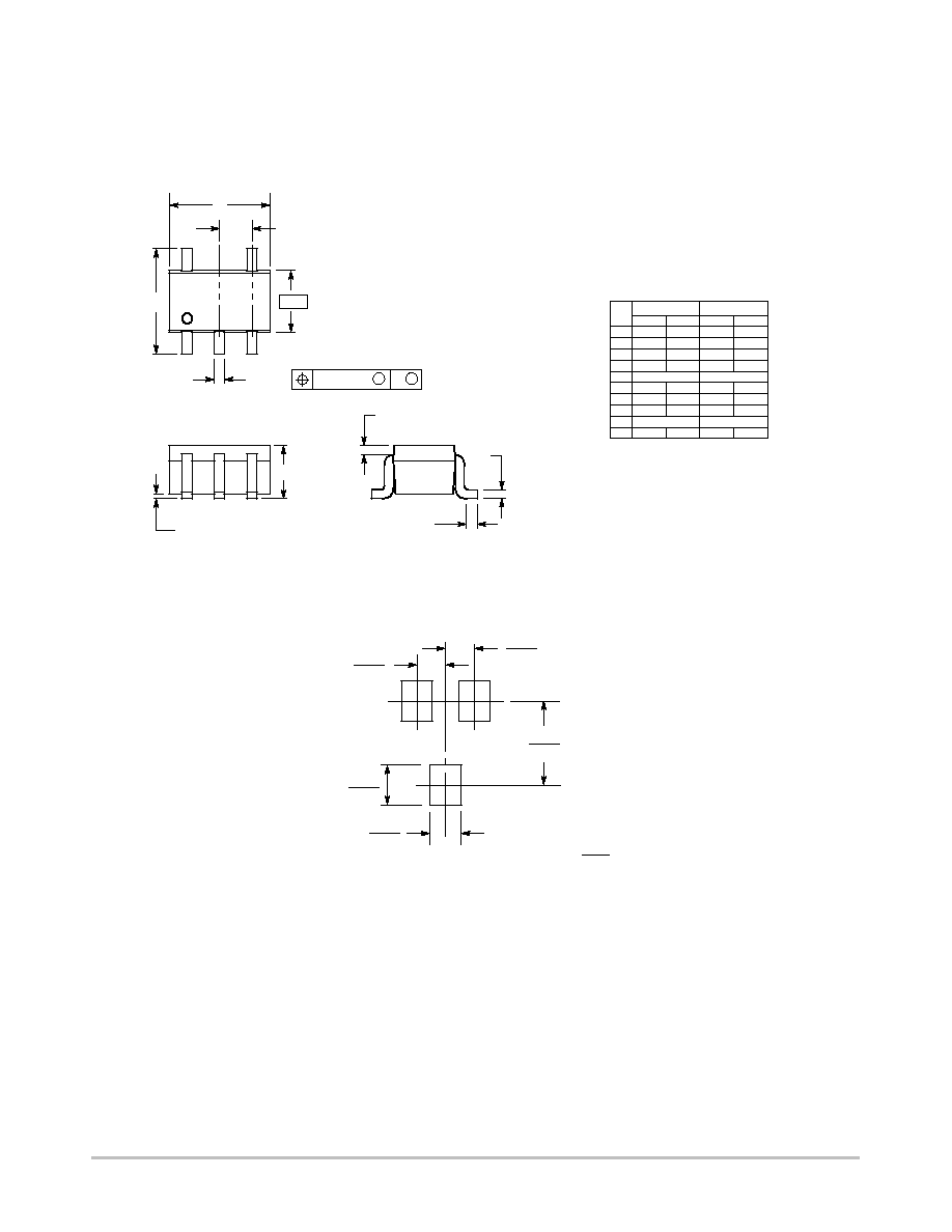
PACKAGE DIMENSIONS
NOTES:
1. DIMENSIONING AND TOLERANCING
PER ANSI Y14.5M, 1982.
2. CONTROLLING DIMENSION: INCH.
3. 419A-01 OBSOLETE. NEW STANDARD
419A-02.
4. DIMENSIONS A AND B DO NOT INCLUDE
MOLD FLASH, PROTRUSIONS, OR GATE
BURRS.
DIM
A
MIN
MAX
MIN
MAX
MILLIMETERS
1.80
2.20
0.071
0.087
INCHES
B
1.15
1.35
0.045
0.053
C
0.80
1.10
0.031
0.043
D
0.10
0.30
0.004
0.012
G
0.65 BSC
0.026 BSC
H
---
0.10
---
0.004
J
0.10
0.25
0.004
0.010
K
0.10
0.30
0.004
0.012
N
0.20 REF
0.008 REF
S
2.00
2.20
0.079
0.087
B
0.2 (0.008)
M
M
1
2
3
4
5
A
G
S
D
5 PL
H
C
N
J
K
-B-
SC-88A, SOT-353, SC-70
CASE 419A-02
ISSUE J
1.9
0.075
0.65
0.025
0.65
0.025
0.9
0.035
0.7
0.028
mm
inches
SCALE 10:1
*For additional information on our Pb-Free strategy and soldering
details, please download the ON Semiconductor Soldering and
Mounting Techniques Reference Manual, SOLDERRM/D.
SOLDERING FOOTPRINT*
NL17SZ07
http://onsemi.com
6
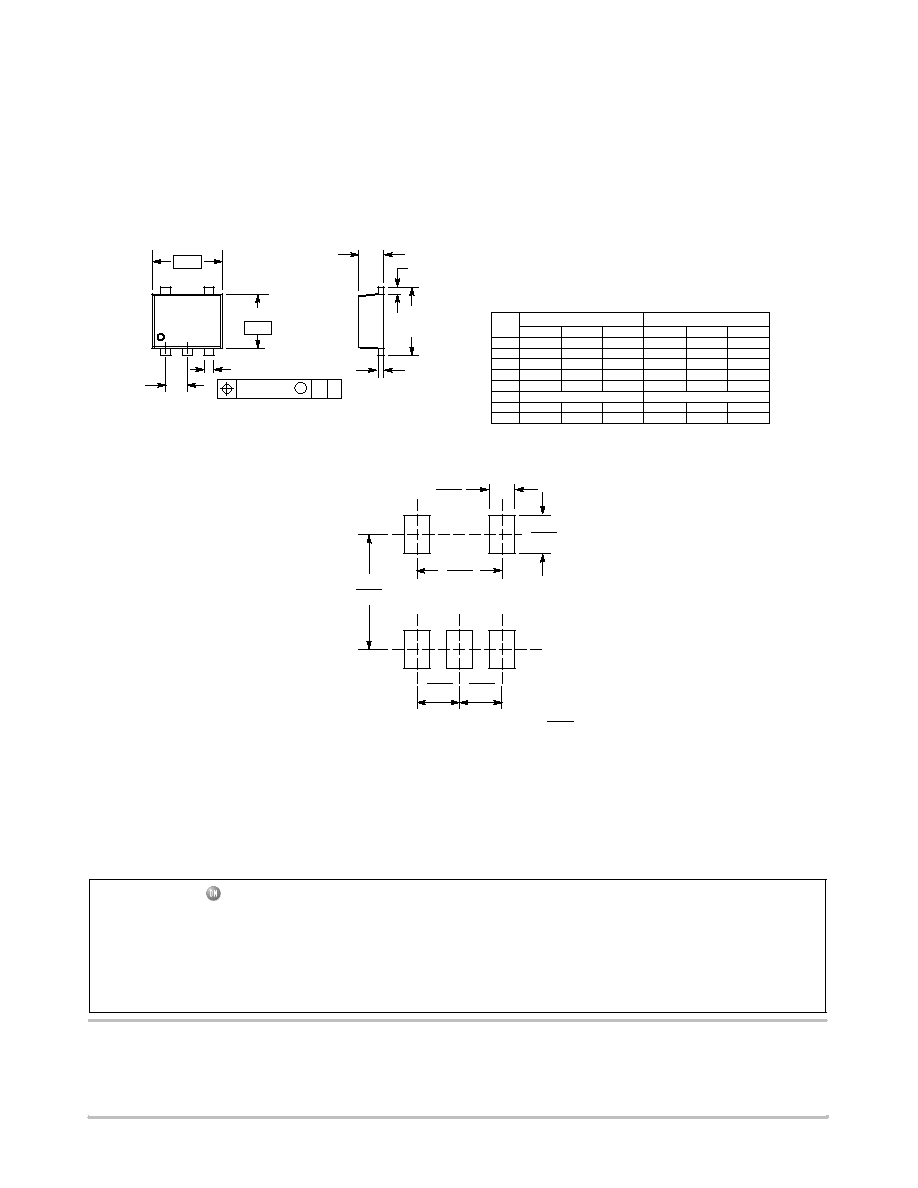
PACKAGE DIMENSIONS
SOT-553, 5 LEAD
CASE 463B-01
ISSUE B
e
M
0.08 (0.003)
X
b
5 PL
A
c
-X-
-Y-
NOTES:
1. DIMENSIONING AND TOLERANCING PER
ANSI Y14.5M, 1982.
2. CONTROLLING DIMENSION: MILLIMETERS
3. MAXIMUM LEAD THICKNESS INCLUDES
LEAD FINISH THICKNESS. MINIMUM LEAD
THICKNESS IS THE MINIMUM THICKNESS
OF BASE MATERIAL.
D
E
Y
1 2
3
4
5
L
1.35
0.0531
0.5
0.0197
mm
inches
SCALE 20:1
0.5
0.0197
1.0
0.0394
0.45
0.0177
0.3
0.0118
*For additional information on our Pb-Free strategy and soldering
details, please download the ON Semiconductor Soldering and
Mounting Techniques Reference Manual, SOLDERRM/D.
SOLDERING FOOTPRINT*
H
E
DIM
A
MIN
NOM
MAX
MIN
MILLIMETERS
0.50
0.55
0.60
0.020
INCHES
b
0.17
0.22
0.27
0.007
c
D
1.50
1.60
1.70
0.059
E
1.10
1.20
1.30
0.043
e
0.50 BSC
L
0.10
0.20
0.30
0.004
0.022
0.024
0.009
0.011
0.063
0.067
0.047
0.051
0.008
0.012
NOM
MAX
1.50
1.60
1.70
0.059
0.063
0.067
H
E
0.08
0.13
0.18
0.003
0.005
0.007
0.020 BSC
ON Semiconductor and are registered trademarks of Semiconductor Components Industries, LLC (SCILLC). SCILLC reserves the right to make changes without further notice
to any products herein. SCILLC makes no warranty, representation or guarantee regarding the suitability of its products for any particular purpose, nor does SCILLC assume any liability
arising out of the application or use of any product or circuit, and specifically disclaims any and all liability, including without limitation special, consequential or incidental damages.
"Typical" parameters which may be provided in SCILLC data sheets and/or specifications can and do vary in different applications and actual performance may vary over time. All
operating parameters, including "Typicals" must be validated for each customer application by customer's technical experts. SCILLC does not convey any license under its patent rights
nor the rights of others. SCILLC products are not designed, intended, or authorized for use as components in systems intended for surgical implant into the body, or other applications
intended to support or sustain life, or for any other application in which the failure of the SCILLC product could create a situation where personal injury or death may occur. Should
Buyer purchase or use SCILLC products for any such unintended or unauthorized application, Buyer shall indemnify and hold SCILLC and its officers, employees, subsidiaries, affiliates,
and distributors harmless against all claims, costs, damages, and expenses, and reasonable attorney fees arising out of, directly or indirectly, any claim of personal injury or death
associated with such unintended or unauthorized use, even if such claim alleges that SCILLC was negligent regarding the design or manufacture of the part. SCILLC is an Equal
Opportunity/Affirmative Action Employer. This literature is subject to all applicable copyright laws and is not for resale in any manner.
PUBLICATION ORDERING INFORMATION
N. American Technical Support: 800-282-9855 Toll Free
USA/Canada
Japan: ON Semiconductor, Japan Customer Focus Center
2-9-1 Kamimeguro, Meguro-ku, Tokyo, Japan 153-0051
Phone: 81-3-5773-3850
NL17SZ07/D
LITERATURE FULFILLMENT:
Literature Distribution Center for ON Semiconductor
P.O. Box 61312, Phoenix, Arizona 85082-1312 USA
Phone: 480-829-7710 or 800-344-3860 Toll Free USA/Canada
Fax: 480-829-7709 or 800-344-3867 Toll Free USA/Canada
Email: orderlit@onsemi.com
ON Semiconductor Website: http://onsemi.com
Order Literature: http://www.onsemi.com/litorder
For additional information, please contact your
local Sales Representative.