 | ÐлекÑÑоннÑй компоненÑ: NZMM7V0T4 | СкаÑаÑÑ:  PDF PDF  ZIP ZIP |
Äîêóìåíòàöèÿ è îïèñàíèÿ www.docs.chipfind.ru
©
Semiconductor Components Industries, LLC, 2002
October, 2002 Rev. 6
1
Publication Order Number:
NZMM7V0T4/D
NZMM7V0T4
EMI Filter with ESD
Protection
Features:
·
4
×
4 mm Lead Less MLF Surface Mount Package
·
9 EMI/RFI Bidirectional "Pi" LowPass Filters
·
ESD Protection Meets IEC600042
·
50 Watt Peak Pulse Power, 8
×
20
ms (all diodes under power)
·
Diode Capacitance: 7 10 pF
·
"Pi" Filter Line Capacitance: 22
±
20% pF
·
Low Zener Diode Leakage: 1
mA Maximum
·
Zener Breakdown Voltage; 6 8 Volts
·
Moisture Sensitivity Level 1
Benefits:
·
Suppresses EMI/RFI Noise in Systems Subjected to Electromagnetic
Interference
·
Small Package Size Minimizes Parasitic Inductance, Thus a More
"Ideal" Low Pass Filtering Response
Typical Applications:
·
Cellular Phones
·
Communication Systems
·
Computers
·
Portable Products with Input/Output Conductors
MAXIMUM RATINGS
Rating
Symbol
Value
Unit
Peak Power Dissipation (Note 1)
8
×
20
m
s Pulse
P
PK
50
Watts
Maximum Junction Temperature
T
J
150
°
C
1. All diodes in parallel under power
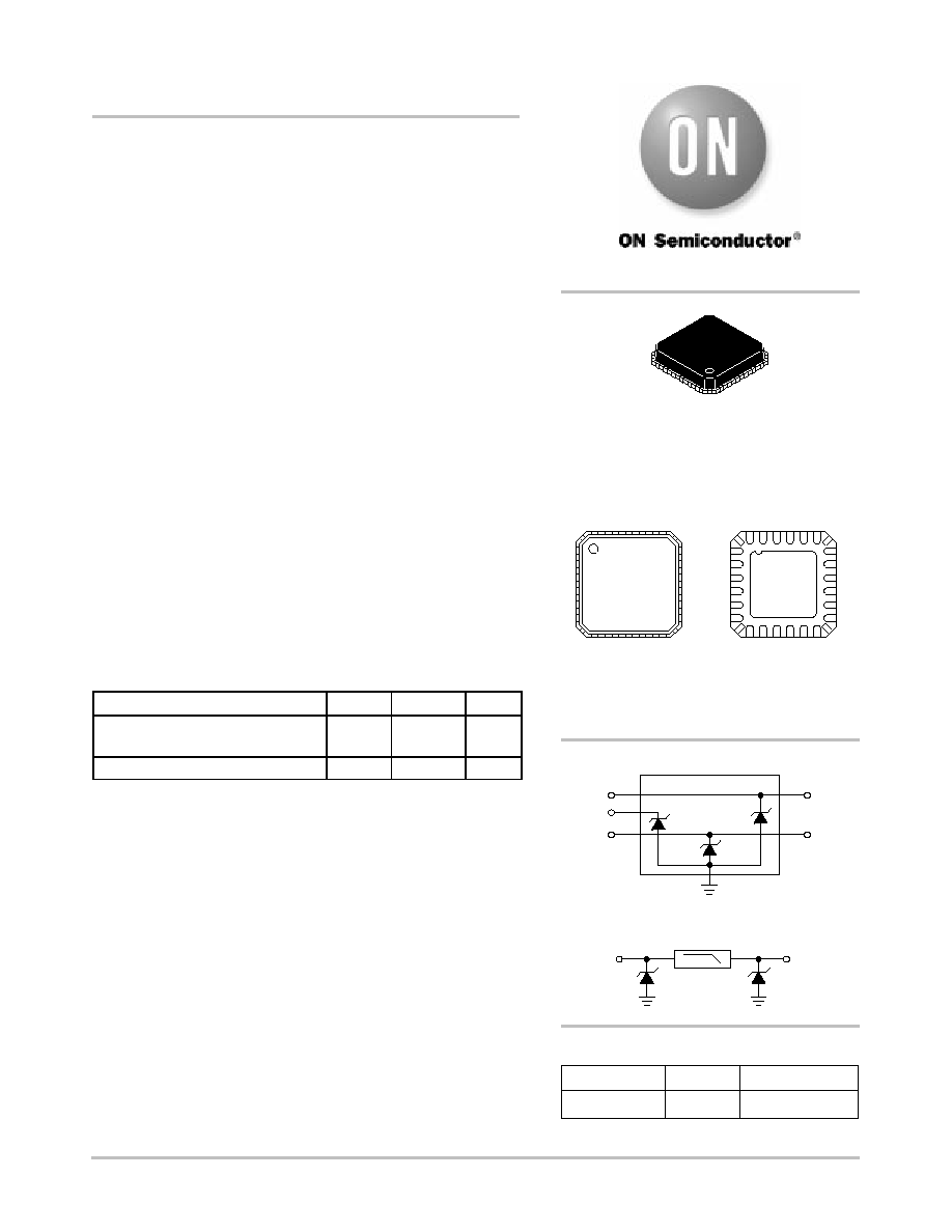
24 PIN MLF
CASE 485F
PLASTIC
ZMM7V = Specific Device Code
ABC
= Date Code
Device
Package
Shipping
ORDERING INFORMATION
NZMM7V0T4
24 PIN
4000/Tape & Reel
LOW PASS FILTER
IN
OUT
IN 1
V
CC
IN 2
OUT 1
OUT 2
USB/RS232 Protection
CIRCUIT DESCRIPTION
18
17
16
15
14
ZMM7V
ABC
MARKING DIAGRAM
13
1
2
3
4
5
6
24
23
22
21
20
19
7
8
9
10
11
12
http://onsemi.com
PINS 421
PINS 1, 3, 2224
(Top View)
(Bottom View)
24
23
22
21
20
19
1
2
3
4
5
6
18
17
16
15
14
13
7
8
9
10
11
12
24
23
22
1
3
Ground
Pad
NZMM7V0T4
http://onsemi.com
2
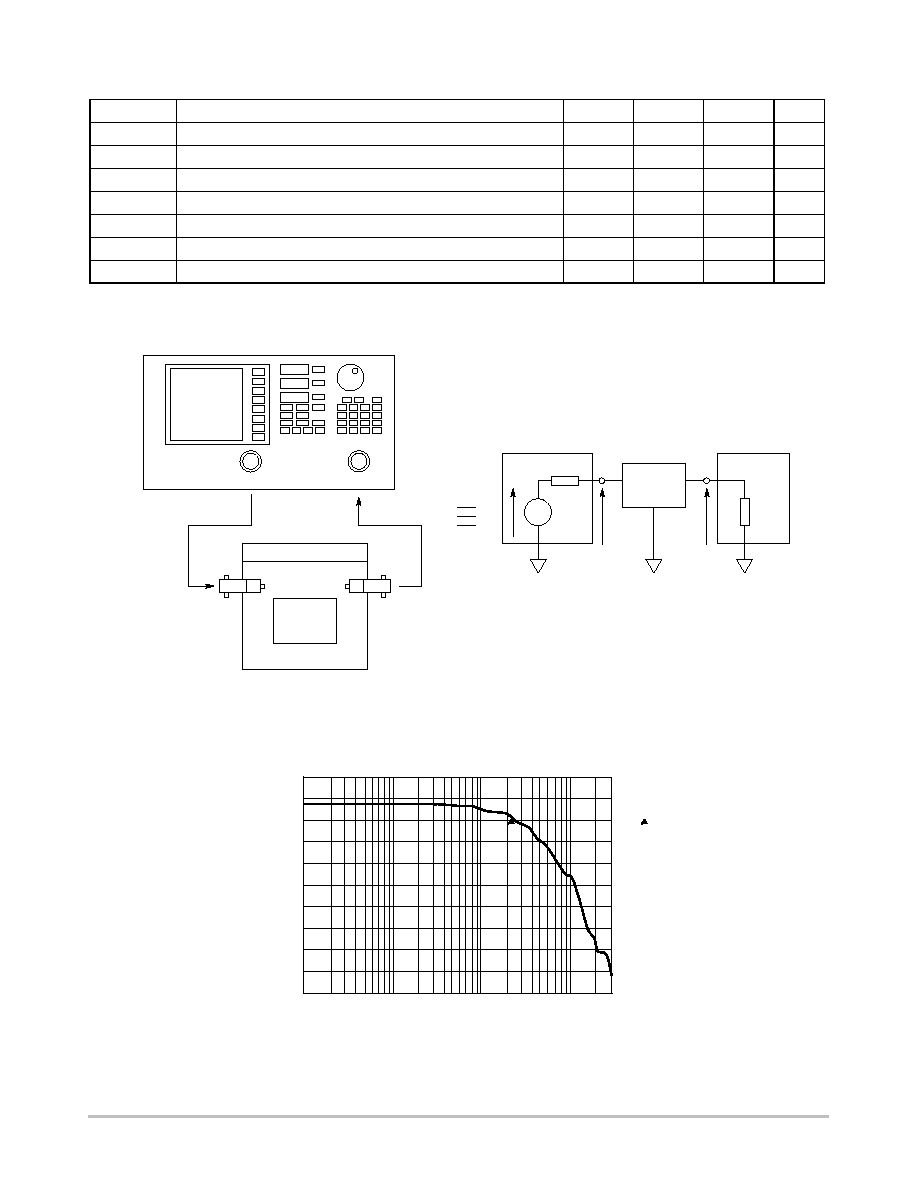
ELECTRICAL CHARACTERISTICS
Symbol
Characteristic
Min
Typ
Max
Unit
V
Z
Zener Breakdown Voltage, @ I
ZT
= 1 mA
6.0
8.0
V
I
r
Zener Leakage Current, @ V
R
= 3 V
N/A
1.0
m
A
V
F
Zener Forward Voltage, @ I
F
= 50 mA
N/A
1.25
V
Capacitance
Zener Internal Capacitance, @ 0 V Bias
7.0
10
pF
Capacitance
Zener/Resistor Array Line Capacitance
17.6
26.4
pF
Resistor
Resistance
90
110
W
F
C
(Note 2)
Cutoff Frequency
220
MHz
2. 50
W
Source and 50
W
Lead Termination per Figure 2
Frequency Response Specification
50
W
50
W
SPECTRUM
ANALYZER
TRACKING
GENERATOR
V
in
V
out
V
G
Test Conditions:
Source Impedance = 50
W
Load Impedance = 50
W
Input Power = 0 dBm
TEST BOARD
TG OUTPUT
RF INPUT
Figure 1. Measurement Conditions
NZMM7V
NZMM7V
Figure 2. Typical EMI Filter Response
(50
W
Source and 50
W
Lead Termination)
GAIN (dB)
1.0
10
100
1000
f, FREQUENCY (MHz)
6.3
3000
10
20
0
30
40
50
Output:
3 dB = 220 MHz
NZMM7V0T4
http://onsemi.com
3
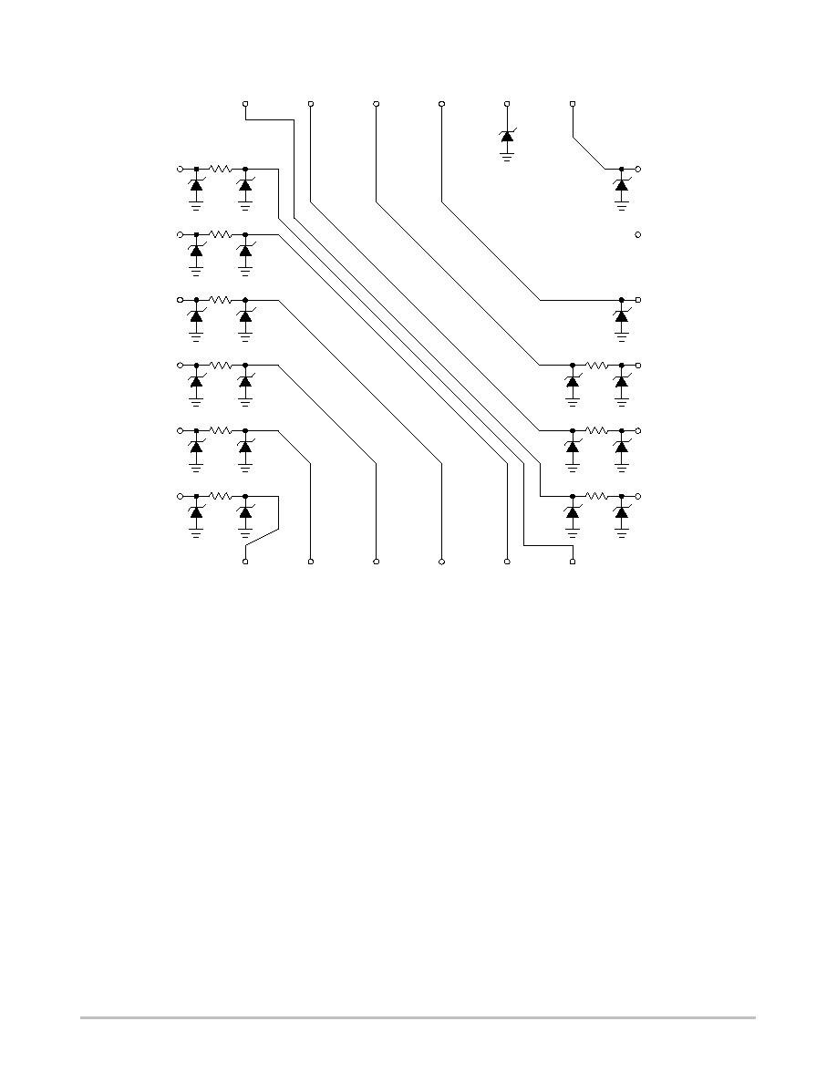
Detailed Device Schematic
18
17
16
15
14
13
12
11
10
9
8
7
6
5
4
3
2
1
NC
24
23
22
21
20
19
Applications Information
Suppressing Noise at the Source
·
Filter all I/O signals leaving the noisy environment
·
Locate I/O driver circuits close to the connector
·
Use the longest rise/fall times possible for all digital signals
Reducing Noise at the Receiver
·
Filter all I/O signals entering the unit
·
Locate the I/O filters as close as possible to the connector
Minimizing Noise Coupling
·
Use multilayer PCBs to minimize power and ground inductance
·
Keep clock circuits away from the I/O connector
·
Ground planes should be used whenever possible
·
Minimize the loop area for all high speed signals
·
Provide for adequate power decoupling
ESD Protection
·
Locate the suppression devices as close to the I/O connector as
possible
·
Minimize the PCB trace length to the suppression device
·
Minimize the PCB trace length for the ground return for the
suppression device
NZMM7V0T4
http://onsemi.com
4
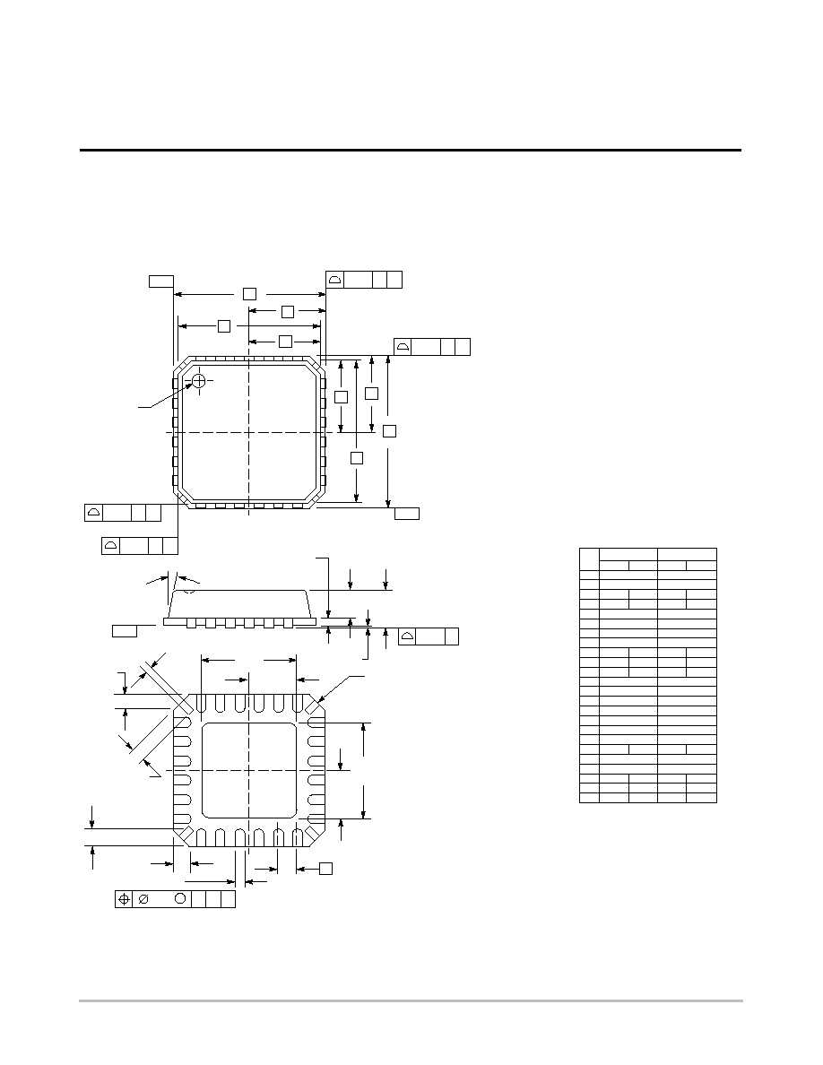
OUTLINE DIMENSIONS
EMI Filter with ESD Protection
Q
X
T
A
0.25
X
AB
C
K
2 PL
H
P
F
T
B
0.25
Y
2 PL
N
R
E
T
Y
0.20
X
2 PL
T
0.20
Y
2 PL
T
NOTE 5 & 6
AA
0.05 T
M
V
AD
Z
W
NOTE 7
AF
4 PL
D
L
T
M
0.10
NOTE 4
X Y
G
AG
4 PL
AF
4 PL
AE
4 PL
DIM
A
MIN
MAX
MIN
MAX
INCHES
4.00 BSC
0.157 BSC
MILLIMETERS
B
C
---
1.00
---
0.039
D
0.18
0.30
0.007
E
3.75 BSC
0.148 BSC
F
3.75 BSC
0.148 BSC
G
0.50 BSC
0.020 BSC
H
2.00 BSC
0.79 BSC
K
0.01
0.05
0.000
0.002
L
0.30
0.55
0.012
0.022
M
---
12
---
N
2.00 BSC
0.079 BSC
P
1.88 BSC
0.074 BSC
Q
0.50 DIA
0.020 DIA
R
1.88 BSC
0.079 BSC
V
2.50 BSC
0.098 BSC
W
1.30 BSC
0.051 BSC
Z
2.50 BSC
0.098 BSC
AA
0.65
0.80
0.026
0.031
AB
0.20 REF
0.008 REF
AD
1.30 BSC
0.051 BSC
AE
0.13
0.23
0.005
0.009
AF
0.24
0.60
0.009
0.024
AG
0.30
0.45
0.012
0.018
NOTES:
1. DIMENSIONING AND TOLERANCING PER ANSI
Y14.5M, 1982.
2. CONTROLLING DIMENSION: MILLIMETERS
3. DIE THICKNESS ALLOWABLE IS 0.305 MM
MAXIMUM (0.012 INCHES MAXIMUM).
4. DIMENSION D APPLIES TO PLATED TERMINAL
AND IS MEASURED BETWEEN 0.20 AND 0.25 MM
FROM TERMINAL.
5. THE PIN #1 IDENTIFIER MUST BE ON THE TOP
SURFACE OF THE PACKAGE BY USING
IDENTIFICATION MARK OR OTHER FEATURE OF
PACKAGE BODY.
6. EXACT SHAPE AND SIZE OF THIS FEATURE IS
OPTIONAL.
7. THE SHAPE SHOWN ON FOUR CORNERS ARE
NOT ACTUAL I/O.
8. PACKAGE WARPAGE MAX 0.05 MM.
24
19
18
13
1
6
7
12
4.00 BSC
0.157 BSC
0.012
°
12
°
24 PIN MLF
PLASTIC PACKAGE
CASE 485F01
ISSUE O

NZMM7V0T4
http://onsemi.com
5
Notes

NZMM7V0T4
http://onsemi.com
6
Notes

NZMM7V0T4
http://onsemi.com
7
Notes
NZMM7V0T4
http://onsemi.com
8
ON Semiconductor and are registered trademarks of Semiconductor Components Industries, LLC (SCILLC). SCILLC reserves the right to make
changes without further notice to any products herein. SCILLC makes no warranty, representation or guarantee regarding the suitability of its products for any
particular purpose, nor does SCILLC assume any liability arising out of the application or use of any product or circuit, and specifically disclaims any and all
liability, including without limitation special, consequential or incidental damages. "Typical" parameters which may be provided in SCILLC data sheets and/or
specifications can and do vary in different applications and actual performance may vary over time. All operating parameters, including "Typicals" must be
validated for each customer application by customer's technical experts. SCILLC does not convey any license under its patent rights nor the rights of others.
SCILLC products are not designed, intended, or authorized for use as components in systems intended for surgical implant into the body, or other applications
intended to support or sustain life, or for any other application in which the failure of the SCILLC product could create a situation where personal injury or death
may occur. Should Buyer purchase or use SCILLC products for any such unintended or unauthorized application, Buyer shall indemnify and hold SCILLC
and its officers, employees, subsidiaries, affiliates, and distributors harmless against all claims, costs, damages, and expenses, and reasonable attorney fees
arising out of, directly or indirectly, any claim of personal injury or death associated with such unintended or unauthorized use, even if such claim alleges that
SCILLC was negligent regarding the design or manufacture of the part. SCILLC is an Equal Opportunity/Affirmative Action Employer.
PUBLICATION ORDERING INFORMATION
JAPAN: ON Semiconductor, Japan Customer Focus Center
291 Kamimeguro, Meguroku, Tokyo, Japan 1530051
Phone: 81357733850
Email: r14525@onsemi.com
ON Semiconductor Website: http://onsemi.com
For additional information, please contact your local
Sales Representative.
NZMM7V0T4/D
Literature Fulfillment:
Literature Distribution Center for ON Semiconductor
P.O. Box 5163, Denver, Colorado 80217 USA
Phone: 3036752175 or 8003443860 Toll Free USA/Canada
Fax: 3036752176 or 8003443867 Toll Free USA/Canada
Email: ONlit@hibbertco.com
N. American Technical Support: 8002829855 Toll Free USA/Canada