 | –≠–ª–µ–∫—Ç—Ä–æ–Ω–Ω—ã–π –∫–æ–º–ø–æ–Ω–µ–Ω—Ç: SA15A | –°–∫–∞—á–∞—Ç—å:  PDF PDF  ZIP ZIP |

©
Semiconductor Components Industries, LLC, 2002
June, 2002 ≠ Rev. 7
1
Publication Order Number:
SA5.0A/D
SA5.0A Series
500 Watt Peak Power
MiniMOSORBE Zener
Transient Voltage
Suppressors
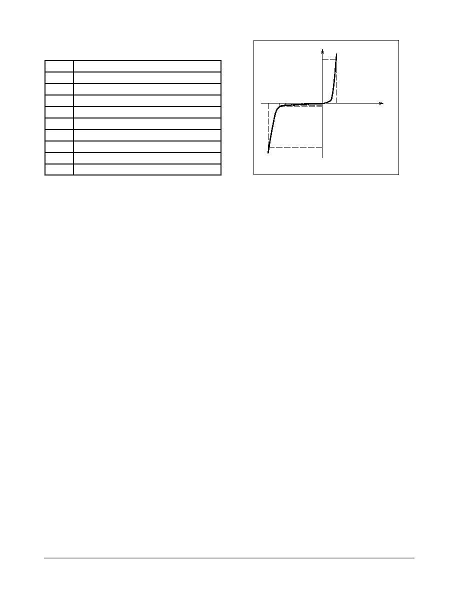
Unidirectional*
The SA5.0A series is designed to protect voltage sensitive
components from high voltage, high energy transients. They have
excellent clamping capability, high surge capability, low zener
impedance and fast response time. The SA5.0A series is supplied in
ON Semiconductor's exclusive, cost-effective, highly reliable
Surmetic
t axial leaded package and is ideally-suited for use in
communication systems, numerical controls, process controls,
medical equipment, business machines, power supplies and many
other industrial/consumer applications.
Specification Features:
∑
Working Peak Reverse Voltage Range ≠ 5 to 170 V
∑
Peak Power ≠ 500 Watts @ 1 ms
∑
ESD Rating of Class 3 (>16 KV) per Human Body Model
∑
Maximum Clamp Voltage @ Peak Pulse Current
∑
Low Leakage < 1
mA above 8.5 V
∑
UL 497B for Isolated Loop Circuit Protection
∑
Maximum Temperature Coefficient Specified
∑
Response Time is typically < 1 ns
Mechanical Characteristics:
CASE:
Void-free, Transfer-molded, Thermosetting plastic
FINISH:
All external surfaces are corrosion resistant and leads are
readily solderable
MAXIMUM LEAD TEMPERATURE FOR SOLDERING:
230
∞
C,
1/16
from the case for 10 seconds
POLARITY:
Cathode indicated by polarity band.
MOUNTING POSITION:
Any
MAXIMUM RATINGS
Rating
Symbol
Value
Unit
Peak Power Dissipation (Note 1)
@ T
L
25
∞
C
P
PK
500
Watts
Steady State Power Dissipation
@ T
L
75
∞
C, Lead Length = 3/8
Derated above T
L
= 75
∞
C
P
D
3.0
30
Watts
mW/
∞
C
Thermal Resistance, Junction≠to≠Lead
R
q
JL
33.3
∞
C/W
Forward Surge Current (Note 2)
@ T
A
= 25
∞
C
I
FSM
70
Amps
Operating and Storage Temperature Range
T
J
, T
stg
≠ 55 to +175
∞
C
1. Nonrepetitive current pulse per Figure 4 and derated above T
A
= 25
∞
C per Fig-
ure 2.
2. 1/2 sine wave (or equivalent square wave), PW = 8.3 ms, duty cycle = 4 pulses
per minute
*Please see SA5.0CA ≠ SA170CA for Bidirectional devices.
Device
Package
Shipping
ORDERING INFORMATION
SAxxxA
Axial Lead
1000 Units/Box
SAxxxARL*
Axial Lead
5000/Tape & Reel
AXIAL LEAD
CASE 59
PLASTIC
L = Assembly Location
SAxxxA = ON Device Code
YY = Year
WW = Work Week
L
SA
xxxA
YYWW
Cathode
Anode
Devices listed in
bold, italic are ON Semiconductor
Preferred devices. Preferred devices are recommended
choices for future use and best overall value.
http://onsemi.com
*SA8.0A, SA130A, and SA160A Not Available in
5000/Tape & Reel.
SA5.0A Series
http://onsemi.com
2
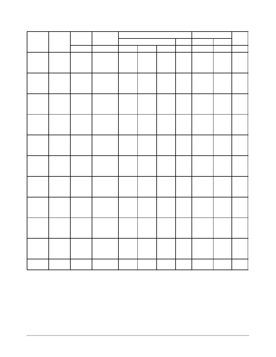
ELECTRICAL CHARACTERISTICS
(T
A
= 25
∞
C unless
otherwise noted, V
F
= 3.5 V Max. @ I
F
(Note 6) = 35 A)
Symbol
Parameter
I
PP
Maximum Reverse Peak Pulse Current
V
C
Clamping Voltage @ I
PP
V
RWM
Working Peak Reverse Voltage
I
R
Maximum Reverse Leakage Current @ V
RWM
V
BR
Breakdown Voltage @ I
T
I
T
Test Current
Q
V
BR
Maximum Temperature Variation of V
BR
I
F
Forward Current
V
F
Forward Voltage @ I
F
Uni≠Directional TVS
I
PP
I
F
V
I
I
R
I
T
V
RWM
V
C
V
BR
V
F
SA5.0A Series
http://onsemi.com
3
ELECTRICAL CHARACTERISTICS
(T
A
= 25
∞
C unless otherwise noted, V
F
= 3.5 V Max. @ I
F
(Note 6)
= 35 A)
V
RWM
Breakdown Voltage
V
C
@ I
PP
(Note 5)
Device
V
RWM
(Note 3)
I
R
@ V
RWM
V
BR
(Note 4) (Volts)
@ I
T
V
C
I
PP
Q
V
BR
Device
Device
Marking
Volts
m
A
Min
Nom
Max
mA
Volts
A
mV/
∞
C
SA5.0A
SA5.0A
5
600
6.4
6.7
7
10
9.2
54.3
5
SA6.0A
SA6.0A
6
600
6.67
7.02
7.37
10
10.3
48.5
5
SA7.0A
SA7.0A
7
150
7.78
8.19
8.6
10
12
41.7
6
SA7.5A
SA7.5A
7.5
50
8.33
8.77
9.21
1
12.9
38.8
7
SA8.0A*
SA8.0A*
8
25
8.89
9.36
9.83
1
13.6
36.7
7
SA8.5A
SA8.5A
8.5
5
9.44
9.92
10.4
1
14.4
34.7
8
SA9.0A
SA9.0A
9
1
10
10.55
11.1
1
15.4
32.5
9
SA10A
SA10A
10
1
11.1
11.7
12.3
1
17
29.4
10
SA11A
SA11A
11
1
12.2
12.85
13.5
1
18.2
27.4
11
SA12A
SA12A
12
1
13.3
14
14.7
1
19.9
25.1
12
SA13A
SA13A
13
1
14.4
15.15
15.9
1
21.5
23.2
13
SA14A
SA14A
14
1
15.6
16.4
17.2
1
23.2
21.5
14
SA15A
SA15A
15
1
16.7
17.6
18.5
1
24.4
20.6
16
SA16A
SA16A
16
1
17.8
18.75
19.7
1
26
19.2
17
SA17A
SA17A
17
1
18.9
19.9
20.9
1
27.6
18.1
19
SA18A
SA18A
18
1
20
21.05
22.1
1
29.2
17.2
20
SA20A
SA20A
20
1
22.2
23.35
24.5
1
32.4
15.4
23
SA22A
SA22A
22
1
24.4
25.65
26.9
1
35.5
14.1
25
SA24A
SA24A
24
1
26.7
28.1
29.5
1
38.9
12.8
28
SA26A
SA26A
26
1
28.9
30.4
31.9
1
42.1
11.9
30
SA28A
SA28A
28
1
31.1
32.75
34.4
1
45.4
11
31
SA30A
SA30A
30
1
33.3
35.05
36.8
1
48.4
10.3
36
SA33A
SA33A
33
1
36.7
38.65
40.6
1
53.3
9.4
39
SA36A
SA36A
36
1
40
42.1
44.2
1
58.1
8.6
41
SA40A
SA40A
40
1
44.4
46.55
49.1
1
64.5
7.8
46
SA43A
SA43A
43
1
47.8
50.3
52.8
1
69.4
7.2
50
SA45A
SA45A
45
1
50
52.65
55.3
1
72.7
6.9
52
SA48A
SA48A
48
1
53.3
56.1
58.9
1
77.4
6.5
56
SA51A
SA51A
51
1
56.7
59.7
62.7
1
82.4
6.1
61
SA58A
SA58A
58
1
64.4
67.8
71.2
1
93.6
5.3
70
SA60A
SA60A
60
1
66.7
70.2
73.7
1
96.8
5.2
71
SA64A
SA64A
64
1
71.1
74.85
78.6
1
103
4.9
76
SA70A
SA70A
70
1
77.8
81.9
86
1
113
4.4
85
SA78A
SA78A
78
1
86.7
91.25
95.8
1
126
4.0
95
SA90A
SA90A
90
1
100
105.5
111
1
146
3.4
110
SA100A
SA100A
100
1
111
117
123
1
162
3.1
123
SA110A
SA110A
110
1
122
128.5
135
1
177
2.8
133
SA120A
SA120A
120
1
133
140
147
1
193
2.5
146
SA130A*
SA130A*
130
1
144
151.5
159
1
209
2.4
158
SA150A
SA150A
150
1
167
176
185
1
243
2.1
184
SA160A*
SA160A*
160
1
178
187.5
197
1
259
1.9
196
SA170A
SA170A
170
1
189
199
209
1
275
1.8
208
NOTES:
3. MiniMOSORB
t
transients suppressor is normally selected according to the maximum working peak reverse voltage (V
RWM
), which
should be equal to or greater than the dc or continuous peak operating voltage level.
4. V
BR
measured at pulse test current I
T
at an ambient temperature of 25
∞
C.
5. Surge current waveform per Figure 4 and derate per Figures 1 and 2.
6. 1/2 sine wave (or equivalent square wave), PW = 8.3 ms, duty cycle = 4 pulses per minute
*Not Available in the 5000/Tape & Reel.
SA5.0A Series
http://onsemi.com
4
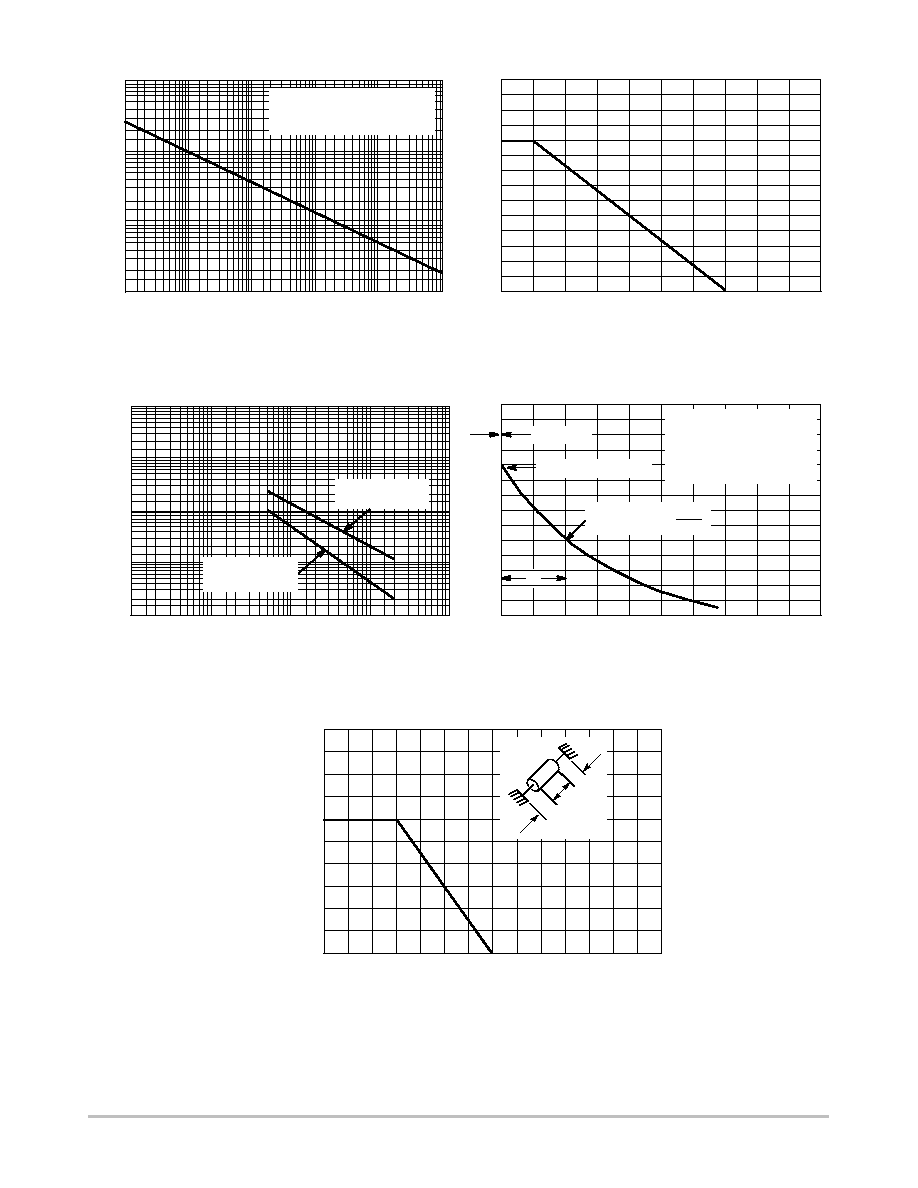
100
10
1
0.1
0.1
m
s
1
m
s
10
m
s
100
m
s
1 ms
10 ms
P P
, PEAK POWER (kW)
t
p
, PULSE WIDTH
Figure 1. Pulse Rating Curve
NONREPETITIVE PULSE
WAVEFORM SHOWN IN
FIGURE 4
100
80
60
40
20
0
0
25
50
75
100
125
150
175
200
PEAK PULSE DERA
TING IN % OF
PEAK POWER OR CURRENT
@
T
A
= 25
C
T
A
, AMBIENT TEMPERATURE (
∞
C)
Figure 2. Pulse Derating Curve
10,000
1000
100
10
0.1
1
10
100
1000
C, CAP
ACIT
ANCE (pF)
V
BR
, BREAKDOWN VOLTAGE (VOLTS)
MEASURED @
ZERO BIAS
Figure 3. Capacitance versus Breakdown Voltage
100
50
0
0
1
2
3
4
t, TIME (ms)
V
ALUE (%)
PULSE WIDTH (t
p
) IS
DEFINED AS THAT POINT
WHERE THE PEAK
CURRENT DECAYS TO
50% OF I
PP
.
PEAK VALUE ≠ I
PP
HALF VALUE ≠
I
PP
2
Figure 4. Pulse Waveform
5
4
3
2
1
0
0 25
50
75 100 125 150 175 200
P
D
, STEADY
ST
A
TE POWER DISSIP
A
TION (W
A
TTS)
T
L
, LEAD TEMPERATURE (
∞
C)
3/8
3/8
Figure 5. Steady State Power Derating
t
r
10
m
s
MEASURED @
(V
RWM
)
t
P
K
∞

SA5.0A Series
http://onsemi.com
5
UL RECOGNITION*
The entire series including the bidirectional CA suffix has
Underwriters Laboratory Recognition for the classification
of protectors (QVGV2) under the UL standard for safety
497B and File #E 116110. Many competitors only have one
or two devices recognized or have recognition in a
non-protective category. Some competitors have no
recognition at all. With the UL497B recognition, our parts
successfully passed several tests including Strike Voltage
Breakdown test, Endurance Conditioning, Temperature test,
Dielectric Voltage-Withstand test, Discharge test and
several more.
Whereas, some competitors have only passed a
flammability test for the package material, we have been
recognized for much more to be included in their protector
category.
*Applies to SA5.0A, CA ≠ SA170A, CA.
SA5.0A Series
http://onsemi.com
6
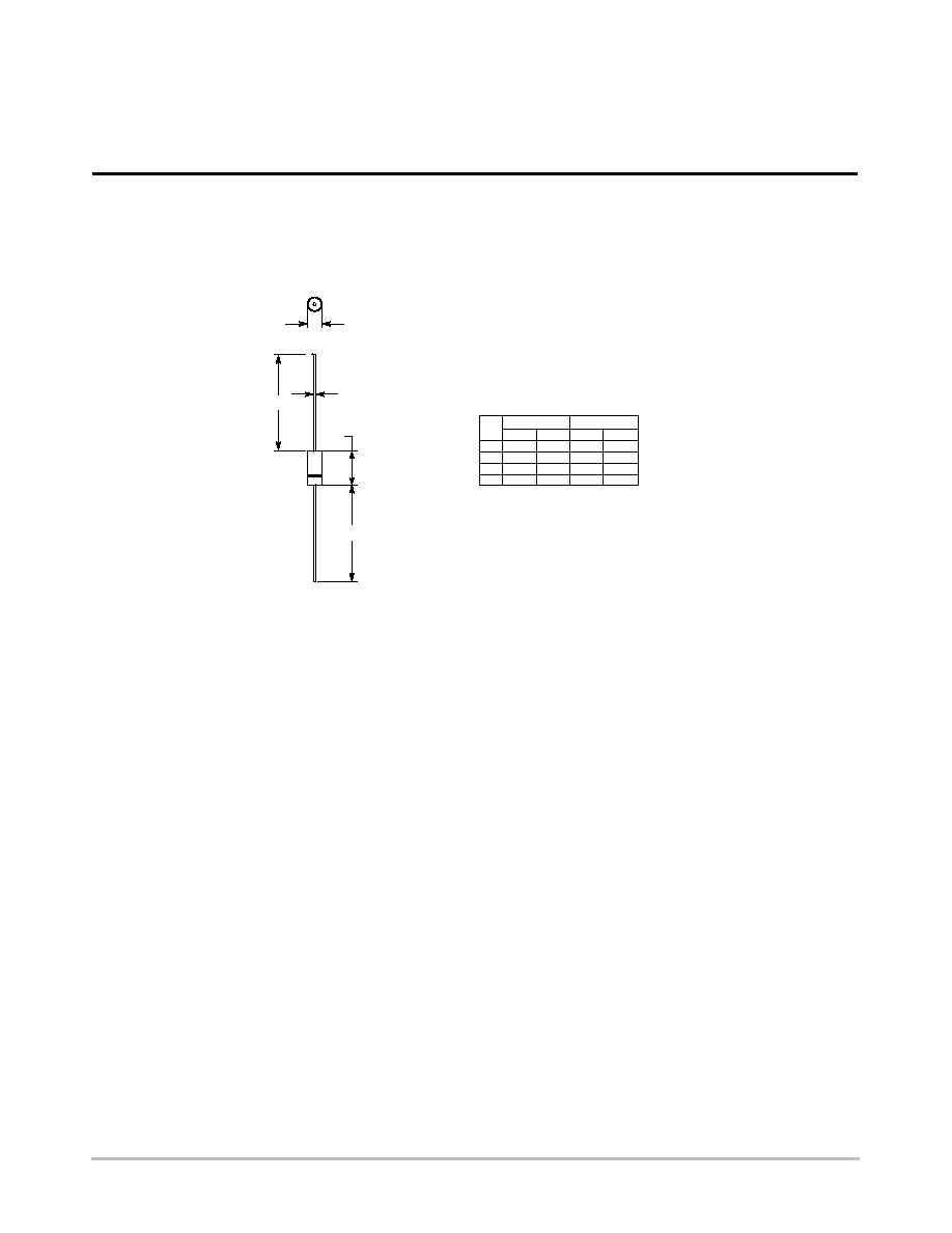
OUTLINE DIMENSIONS
500 Watt Peak Power MiniMOSORB
TM
Transient Voltage Suppressors ≠ Axial Leaded
MINI MOSORB
CASE 59≠09
ISSUE S
K
A
D
K
B
DIM
MIN
MAX
MIN
MAX
MILLIMETERS
INCHES
A
5.80
7.60
0.228
0.299
B
2.60
3.60
0.102
0.142
D
0.71
0.86
0.028
0.034
K
25.44
---
1.000
---
NOTES:
1. DIMENSIONING AND TOLERANCING PER ANSI
Y14.5M, 1982.
2. CONTROLLING DIMENSION: INCH.
3. 59-04 OBSOLETE, NEW STANDARD 59-09.
4. 59-03 OBSOLETE, NEW STANDARD 59-10.
5. ALL RULES AND NOTES ASSOCIATED WITH
JEDEC DO-41 OUTLINE SHALL APPLY.
6. POLARITY DENOTED BY CATHODE BAND.
7. LEAD DIAMETER NOT CONTROLLED WITHIN F
DIMENSION.

SA5.0A Series
http://onsemi.com
7
Notes
SA5.0A Series
http://onsemi.com
8
ON Semiconductor and are registered trademarks of Semiconductor Components Industries, LLC (SCILLC). SCILLC reserves the right to make
changes without further notice to any products herein. SCILLC makes no warranty, representation or guarantee regarding the suitability of its products for any
particular purpose, nor does SCILLC assume any liability arising out of the application or use of any product or circuit, and specifically disclaims any and all
liability, including without limitation special, consequential or incidental damages. "Typical" parameters which may be provided in SCILLC data sheets and/or
specifications can and do vary in different applications and actual performance may vary over time. All operating parameters, including "Typicals" must be
validated for each customer application by customer's technical experts. SCILLC does not convey any license under its patent rights nor the rights of others.
SCILLC products are not designed, intended, or authorized for use as components in systems intended for surgical implant into the body, or other applications
intended to support or sustain life, or for any other application in which the failure of the SCILLC product could create a situation where personal injury or death
may occur. Should Buyer purchase or use SCILLC products for any such unintended or unauthorized application, Buyer shall indemnify and hold SCILLC
and its officers, employees, subsidiaries, affiliates, and distributors harmless against all claims, costs, damages, and expenses, and reasonable attorney fees
arising out of, directly or indirectly, any claim of personal injury or death associated with such unintended or unauthorized use, even if such claim alleges that
SCILLC was negligent regarding the design or manufacture of the part. SCILLC is an Equal Opportunity/Affirmative Action Employer.
PUBLICATION ORDERING INFORMATION
JAPAN: ON Semiconductor, Japan Customer Focus Center
4≠32≠1 Nishi≠Gotanda, Shinagawa≠ku, Tokyo, Japan 141≠0031
Phone: 81≠3≠5740≠2700
Email: r14525@onsemi.com
ON Semiconductor Website: http://onsemi.com
For additional information, please contact your local
Sales Representative.
SA5.0A/D
MiniMOSORB and Surmetic are trademarks of Semiconductor Components Industries, LLC.
Literature Fulfillment:
Literature Distribution Center for ON Semiconductor
P.O. Box 5163, Denver, Colorado 80217 USA
Phone: 303≠675≠2175 or 800≠344≠3860 Toll Free USA/Canada
Fax: 303≠675≠2176 or 800≠344≠3867 Toll Free USA/Canada
Email: ONlit@hibbertco.com
N. American Technical Support: 800≠282≠9855 Toll Free USA/Canada