 | –≠–ª–µ–∫—Ç—Ä–æ–Ω–Ω—ã–π –∫–æ–º–ø–æ–Ω–µ–Ω—Ç: SMF12AT1 | –°–∫–∞—á–∞—Ç—å:  PDF PDF  ZIP ZIP |
©
Semiconductor Components Industries, LLC, 2003
March, 2003 - Rev. 0
1
Publication Order Number:
SMF5.0AT1/D
SMF5.0AT1 Series
Zener Transient
Voltage Suppressor
SOD-123 Flat Lead Package
The SMF5.0A Series is designed to protect voltage sensitive
components from high voltage, high energy transients. Excellent
clamping capability, high surge capability, low zener impedance and
fast response time. Because of its small size, it is ideal for use in
cellular phones, portable devices, business machines, power supplies
and many other industrial/consumer applications.
Specification Features:
∑
Stand-of f Voltage: 5 - 170 Volts
∑
Peak Power - 200 Watts @ 1 ms (SMF5.0A - SMF58A)
Peak Power
- 175 Watts @ 1 ms (SMF60A - SMF170A)
∑
Maximum Clamp Voltage @ Peak Pulse Current
∑
Low Leakage
∑
Response Time is Typically < 1 ns
∑
ESD Rating of Class 3 (> 16 kV) per Human Body Model
IEC61000-4-2 Level 4 ESD Protection
IEC61000-4-4 40 A ESD Protection
∑
Low Profile - Maximum Height of 1.0 mm
∑
Small Footprint - Footprint Area of 8.45 mm
2
∑
Supplied in 8 mm Tape and Reel - 3,000 Units per Reel
∑
Cathode Indicated by Polarity Band
Mechanical Characteristics:
CASE:
Void-free, transfer-molded, thermosetting plastic
Epoxy Meets UL94, VO
LEAD FINISH:
100% Matte Sn (Tin)
MOUNTING POSITION:
Any
QUALIFIED MAX REFLOW TEMPERATURE:
260
∞
C
Device Meets MSL 1 Requirements
PLASTIC SURFACE MOUNT
ZENER OVERVOLTAGE
TRANSIENT SUPPRESSOR
5 - 170 VOLTS
200 WATT PEAK POWER
Device
Package
Shipping
ORDERING INFORMATION
SMFxxxAT1
SOD-123FL
3,000/Tape & Reel
1
2
1: CATHODE
2: ANODE
LEAD ORIENTATION IN TAPE:
Cathode Lead to Sprocket Holes
http://onsemi.com
SOD-123FL
CASE 498
PLASTIC
MARKING DIAGRAM
1
CATHODE
2
ANODE
XX
D
XX = Specific Device Code
D
= Date Code

Uni-Directional TVS
I
PP
I
F
V
I
I
R
I
T
V
RWM
V
C
V
BR
V
F
SMF5.0AT1 Series
http://onsemi.com
2
MAXIMUM RATINGS
Rating
Symbol
Value
Unit
Maximum P
pk
Dissipation (PW-10/1000
m
s) (Note 1) SMF60A - SMF170A
P
pk
175
W
Maximum P
pk
Dissipation (PW-10/1000
m
s) (Note 1) SMF5.0A - SMF58A
P
pk
200
W
Maximum P
pk
Dissipation @ T
A
= 25
∞
C, (PW-8/20
m
s) (Note 2)
P
pk
1000
W
DC Power Dissipation @ T
A
= 25
∞
C (Note 3)
Derate above 25
∞
C
Thermal Resistance from Junction to Ambient (Note 3)
∞
P
D
∞
R
JA
385
4.0
325
∞
mW
mW/
∞
C
∞
C/W
Thermal Resistance from Junction to Lead (Note 3)
R
Jcathode
26
∞
C/W
Operating and Storage Temperature Range
T
J
, T
stg
-55 to +150
∞
C
1. Non-repetitive current pulse at T
A
= 25
∞
C, per waveform of Figure 2.
2. Non-repetitive current pulse at T
A
= 25
∞
C, per waveform of Figure 3.
3. Mounted with recommended minimum pad size, DC board FR-4.
ELECTRICAL CHARACTERISTICS
(T
A
= 25
∞
C unless
otherwise noted, V
F
= 3.5 V Max. @ I
F
(Note 4) = 12 A)
Symbol
Parameter
I
PP
Maximum Reverse Peak Pulse Current
V
C
Clamping Voltage @ I
PP
V
RWM
Working Peak Reverse Voltage
I
R
Maximum Reverse Leakage Current @ V
RWM
V
BR
Breakdown Voltage @ I
T
I
T
Test Current
I
F
Forward Current
V
F
Forward Voltage @ I
F
4. 1/2 sine wave (or equivalent square wave), PW = 8.3 ms,
duty cycle = 4 pulses per minute maximum.

SMF5.0AT1 Series
http://onsemi.com
3
ELECTRICAL CHARACTERISTICS
(T
L
= 30
∞
C unless otherwise noted, V
F
= 1.25 Volts @ 200 mA)
V
RWM
(V)
V
BR
@ I
T
(V) (Note 6)
I
T
I
R
@ V
RWM
V
C(Max)
I
PP(Max)
(A)
Device
Marking
(Note 5)
Min
Nom
Max
(mA)
(
m
A)
(V)
(Note 7)
SMF5.0A
KE
5
6.4
6.7
7
10
400
9.2
21.7
SMF6.0A
KG
6
6.67
7.02
7.37
10
400
10.3
19.4
SMF6.5A
KK
6.5
7.22
7.6
7.98
10
250
11.2
17.9
SMF7.0A
KM
7
7.78
8.2
8.6
10
100
12
16.7
SMF7.5A
KP
7.5
8.33
8.77
9.21
1
50
12.9
15.5
SMF8.0A
KR
8
8.89
9.36
9.83
1
25
13.6
14.7
SMF8.5A
KT
8.5
9.44
9.92
10.4
1
10
14.4
13.9
SMF9.0A
KV
9
10
10.55
11.1
1
5
15.4
13.0
SMF10A
KX
10
11.1
11.7
12.3
1
2.5
17
11.8
SMF11A
KZ
11
12.2
12.85
13.5
1
2.5
18.2
11.0
SMF12A
LE
12
13.3
14
14.7
1
2.5
19.9
10.1
SMF13A
LG
13
14.4
15.15
15.9
1
1
21.5
9.3
SMF14A
LK
14
15.6
16.4
17.2
1
1
23.2
8.6
SMF15A
LM
15
16.7
17.6
18.5
1
1
24.4
8.2
SMF16A
LP
16
17.8
18.75
19.7
1
1
26
7.7
SMF17A
LR
17
18.9
19.9
20.9
1
1
27.6
7.2
SMF18A
LT
18
20
21
22.1
1
1
29.2
6.8
SMF20A
LV
20
22.2
23.35
24.5
1
1
32.4
6.2
SMF22A
LX
22
24.4
25.6
26.9
1
1
35.5
5.6
SMF24A
LZ
24
26.7
28.1
29.5
1
1
38.9
5.1
SMF26A
ME
26
28.9
30.4
31.9
1
1
42.1
4.8
SMF28A
MG
28
31.1
32.8
34.4
1
1
45.4
4.4
SMF30A
MK
30
33.3
35.1
36.8
1
1
48.4
4.1
SMF33A
MM
33
36.7
38.7
40.6
1
1
53.3
3.8
SMF36A
MP
36
40
42.1
44.2
1
1
58.1
3.4
SMF40A
MR
40
44.4
46.8
49.1
1
1
64.5
3.1
SMF43A
MT
43
47.8
50.3
52.8
1
1
69.4
2.9
SMF45A
MV
45
50
52.65
55.3
1
1
72.7
2.8
SMF48A
MX
48
53.3
56.1
58.9
1
1
77.4
2.6
SMF51A
MZ
51
56.7
59.7
62.7
1
1
82.4
2.4
SMF54A
NE
54
60
63.15
66.3
1
1
87.1
2.3
SMF58A
NG
58
64.4
67.8
71.2
1
1
93.6
2.1
SMF60A
NK
60
66.7
70.2
73.7
1
1
96.8
1.8
SMF64A
NM
64
71.1
74.85
78.6
1
1
103
1.7
SMF70A
NP
70
77.8
81.9
86
1
1
113
1.5
SMF75A
NR
75
83.3
87.7
92.1
1
1
121
1.4
SMF78A
NT
78
86.7
91.25
95.8
1
1
126
1.4
SMF85A
NV
85
94.4
99.2
104
1
1
137
1.3
SMF90A
NX
90
100
105.5
111
1
1
146
1.2
SMF100A
NZ
100
111
117
123
1
1
162
1.1
SMF110A
PE
110
122
128.5
135
1
1
177
1.0
SMF120A
PG
120
133
140
147
1
1
193
0.9
SMF130A
PK
130
144
151.5
159
1
1
209
0.8
SMF150A
PM
150
167
176
185
1
1
243
0.7
SMF160A
PP
160
178
187.5
197
1
1
259
0.7
SMF170A
PR
170
189
199
209
1
1
275
0.6
5. A transient suppressor is normally selected according to the Working Peak Reverse Voltage (V
RWM
) which should be equal to or greater
than the DC or continuous peak operating voltage level.
6. V
BR
measured at pulse test current I
T
at ambient temperature of 25
∞
C.
7. Surge current waveform per Figure 2 and derate per Figure 3.

SMF5.0AT1 Series
http://onsemi.com
4
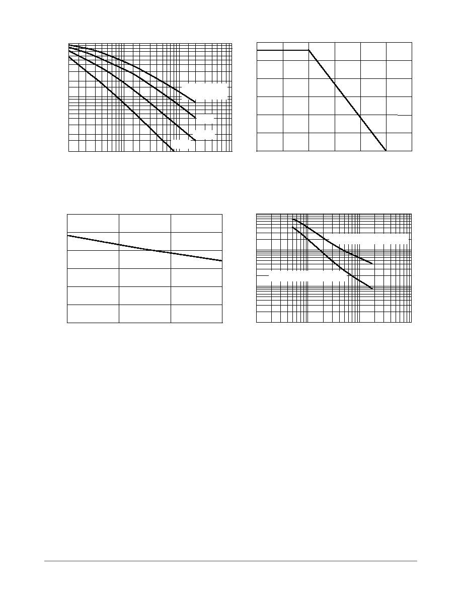
t
P
, PULSE WIDTH (
m
s)
100
1000
10,000
1.0
10
100
10
0
1
2
3
4
0
50
100
t, TIME (ms)
V
ALUE (%)
HALF VALUE -
I
RSM
2
PEAK VALUE - I
RSM
t
r
TYPICAL PROTECTION CIRCUIT
V
in
V
L
Z
in
LOAD
t
P
PULSE WIDTH (t
P
) IS DEFINED
AS THAT POINT WHERE THE PEAK
CURRENT DECAYS TO 50%
OF I
RSM
.
Figure 1. Pulse Rating Curve
Figure 2. 10 X 1000
m
s Pulse Waveform
1000
10,000
Figure 3. 8 X 20
m
s Pulse Waveform
P
P
, PEAK POWER (W
A
TTS)
t
r
10
µ
s
100
80
60
40
20
0
0
25
50
75
100
125
150
T
A
, AMBIENT TEMPERATURE (
∞
C)
120
140
160
Figure 4. Pulse Derating Curve
PEAK PULSE DERA
TING IN % OF
PEAK POWER OR CURRENT @ T
A
= 25
∞
C
100
90
80
70
60
50
40
30
20
10
0
0
20
40
60
80
t, TIME (
m
s)
% OF PEAK PULSE CURRENT
t
P
t
r
PULSE WIDTH (t
P
) IS DEFINED
AS THAT POINT WHERE THE
PEAK CURRENT DECAY = 8 ms
PEAK VALUE I
RSM
@ 8 ms
HALF VALUE I
RSM
/2 @ 20 ms
SMF5.0AT1 Series
http://onsemi.com
5
1.2
1.0
0.8
0.6
0.4
0.2
0
-55
25
85
150
T, TEMPERATURE (
∞
C)
V
,
TYPICAL
FOR
W
ARD VOL
T
AGE (VOL
TS)
F
25
50
75
100
125
175
2.5
2
1.5
1
0
T, TEMPERATURE (
∞
C)
P
, MAXIMUM POWER DISSIP
A
TION (W)
D
0.5
T
L
150
3
1000
100
1
1
10
1000
WORKING PEAK REVERSE VOLTAGE (VOLTS)
C, CAP
ACIT
ANCE (pF)
MEASURED @ 50% V
RWM
MEASURED @ ZERO BIAS
Figure 5. Typical Derating Factor for Duty Cycle
DERA
TING F
ACT
OR
1 ms
10
µ
s
1
0.7
0.5
0.3
0.05
0.1
0.2
0.01
0.02
0.03
0.07
100
µ
s
0.1 0.2
0.5
2
5
10
50
1
20
100
D, DUTY CYCLE (%)
PULSE WIDTH
10 ms
Figure 6. Steady State Power Derating
Figure 7. Forward Voltage
Figure 8. Capacitance versus Working Peak
Reverse Voltage
10
100
SMF5.0AT1 Series
http://onsemi.com
6
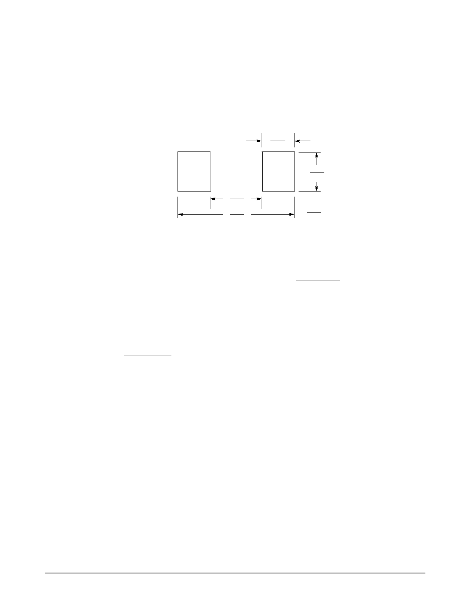
INFORMATION FOR USING THE SOD-123 FLAT LEAD SURFACE MOUNT PACKAGE
MINIMUM RECOMMENDED FOOTPRINT FOR SURFACE MOUNTED APPLICATIONS
Surface mount board layout is a critical portion of the
total design. The footprint for the semiconductor packages
must be the correct size to insure proper solder connection
interface between the board and the package. With the
correct pad geometry, the packages will self align when
subjected to a solder reflow process.
RECOMMENDED FOOTPRINT FOR SOD-123FL
………
………
………
………
………
………
………
………
………
………
mm
inches
0.91
0.036
1.22
0.048
2.36
0.093
4.19
0.165
POWERMITE POWER DISSIPATION
The power dissipation of the SOD-123 Flat Lead is a
function of the mounting pad size. This can vary from the
minimum pad size for soldering to a pad size given for
maximum power dissipation. Power dissipation for a
surface mount device is determined by T
J(max)
, the
maximum rated junction temperature of the die, R
JA
, the
thermal resistance from the device junction to ambient, and
the operating temperature, T
A
. Using the values provided
on the data sheet for the SOD-123 Flat Lead package, P
D
can be calculated as follows:
P
D
=
T
J(max)
- T
A
R
JA
The values for the equation are found in the maximum
ratings table on the data sheet. Substituting these values
into the equation for an ambient temperature T
A
of 25
∞
C,
one can calculate the power dissipation of the device which
in this case is 385 milliwatts.
P
D
= 150
∞
C - 25
∞
C = 385 milliwatts
325
∞
C/W
The 325
∞
C/W for the SOD-123 Flat Lead package
assumes the use of the recommended footprint on a glass
epoxy printed circuit board to achieve a power dissipation
of 385 milliwatts. There are other alternatives to achieving
higher power dissipation from the SOD-123 Flat Lead
package. Another alternative would be to use a ceramic
substrate or an aluminum core board such as Thermal
Clad
Æ
. Using a board material such as Thermal Clad, an
aluminum core board, the power dissipation can be doubled
using the same footprint.
SOLDERING PRECAUTIONS
The melting temperature of solder is higher than the rated
temperature of the device. When the entire device is heated
to a high temperature, failure to complete soldering within
a short time could result in device failure. Therefore, the
following items should always be observed in order to
minimize the thermal stress to which the devices are
subjected.
∑
Always preheat the device.
∑
The delta temperature between the preheat and
soldering should be 100
∞
C or less.*
∑
When preheating and soldering, the temperature of the
leads and the case must not exceed the maximum
temperature ratings as shown on the data sheet. When
using infrared heating with the reflow soldering
method, the difference shall be a maximum of 10
∞
C.
∑
The soldering temperature and time shall not exceed
260
∞
C for more than 10 seconds.
∑
When shifting from preheating to soldering, the
maximum temperature gradient shall be 5
∞
C or less.
∑
After soldering has been completed, the device should
be allowed to cool naturally for at least three minutes.
Gradual cooling should be used as the use of forced
cooling will increase the temperature gradient and
result in latent failure due to mechanical stress.
∑
Mechanical stress or shock should not be applied
during cooling.
* Soldering a device without preheating can cause excessive
thermal shock and stress which can result in damage to the
device.

SMF5.0AT1 Series
http://onsemi.com
7
OUTLINE DIMENSIONS
Transient Voltage Suppressor - Surface Mounted
SOD-123FL
CASE 498-01
ISSUE O
NOTES:
1. DIMENSIONING AND TOLERANCING PER ANSI
Y14.5M, 1982.
2. CONTROLLING DIMENSION: MILLIMETER.
3. DIMENSIONS A AND B DO NOT INCLUDE MOLD
FLASH.
4. DIMENSIONS D AND J ARE TO BE MEASURED
ON FLAT SECTION OF THE LEAD: BETWEEN 0.10
AND 0.25 MM FROM THE LEAD TIP.
A
B
K
D
C
H
E
L
J
L
DIM
MIN
MAX
MIN
MAX
INCHES
MILLIMETERS
A
1.50
1.80
0.059
0.071
B
2.50
2.90
0.098
0.114
C
0.90
1.00
0.039
D
0.70
1.10
0.028
0.043
E
0.55
0.95
0.022
0.037
H
0.00
0.10
0.000
0.004
J
0.10
0.20
0.004
0.008
K
3.40
3.80
0.134
0.150
L
0
8
∞
∞
0
8
∞
∞
POLARITY INDICATOR
OPTIONAL AS NEEDED
0.035
200 Watt Peak Power
SMF5.0AT1 Series
http://onsemi.com
8
ON Semiconductor and are registered trademarks of Semiconductor Components Industries, LLC (SCILLC). SCILLC reserves the right to make
changes without further notice to any products herein. SCILLC makes no warranty, representation or guarantee regarding the suitability of its products for any
particular purpose, nor does SCILLC assume any liability arising out of the application or use of any product or circuit, and specifically disclaims any and all
liability, including without limitation special, consequential or incidental damages. "Typical" parameters which may be provided in SCILLC data sheets and/or
specifications can and do vary in different applications and actual performance may vary over time. All operating parameters, including "Typicals" must be
validated for each customer application by customer's technical experts. SCILLC does not convey any license under its patent rights nor the rights of others.
SCILLC products are not designed, intended, or authorized for use as components in systems intended for surgical implant into the body, or other applications
intended to support or sustain life, or for any other application in which the failure of the SCILLC product could create a situation where personal injury or death
may occur. Should Buyer purchase or use SCILLC products for any such unintended or unauthorized application, Buyer shall indemnify and hold SCILLC
and its officers, employees, subsidiaries, affiliates, and distributors harmless against all claims, costs, damages, and expenses, and reasonable attorney fees
arising out of, directly or indirectly, any claim of personal injury or death associated with such unintended or unauthorized use, even if such claim alleges that
SCILLC was negligent regarding the design or manufacture of the part. SCILLC is an Equal Opportunity/Affirmative Action Employer.
PUBLICATION ORDERING INFORMATION
JAPAN: ON Semiconductor, Japan Customer Focus Center
2-9-1 Kamimeguro, Meguro-ku, Tokyo, Japan 153-0051
Phone: 81-3-5773-3850
ON Semiconductor Website: http://onsemi.com
For additional information, please contact your local
Sales Representative.
SMF5.0AT1/D
Thermal Clad is a registered trademark of the Bergquist Company.
Literature Fulfillment:
Literature Distribution Center for ON Semiconductor
P.O. Box 5163, Denver, Colorado 80217 USA
Phone: 303-675-2175 or 800-344-3860 Toll Free USA/Canada
Fax: 303-675-2176 or 800-344-3867 Toll Free USA/Canada
Email: ONlit@hibbertco.com
N. American Technical Support: 800-282-9855 Toll Free USA/Canada