 | ÐлекÑÑоннÑй компоненÑ: SMS05CT1 | СкаÑаÑÑ:  PDF PDF  ZIP ZIP |
SMS05C
©
Semiconductor Components Industries, LLC, 2003
August, 2003 - Rev. 2
1
Publication Order Number:
SMS05C/D
SMS05C, SMS12C, SMS15C,
SMS24C
5 Line Transient Voltage
Suppressor Array
This 5-line voltage transient suppressor array is designed for
application requiring transient voltage protection capability. It is
intended for use in over-transient voltage and ESD sensitive
equipment such as computers, printers, automotive electronics,
networking communication and other applications. This device
features a monolithic common cathode design which protects five
independent lines in a single SC-74 package.
Features
·
Protects up to 5 Line in a Single SC-74 Package
·
Peak Power Dissipation - 350 W (8 X20
ms Waveform)
·
ESD Rating of Class 3B (Exceeding 8 kV) per Human Body Model
and Class C (Exceeding 400 V) per Machine Model.
·
Compliance with IEC 61000-4-2 (ESD) 15 kV (Air), 8 kV (Contact)
·
UL Flammability Rating of 94V-0
Applications
·
Hand Held Portable Applications
·
Networking and Telecom
·
Automotive Electronics
·
Serial and Parallel Ports
·
Notebooks, Desktops, Servers
MAXIMUM RATINGS
(T
J
=25
°
C unless otherwise specified)
Symbol
Rating
Value
Unit
P
PK
1
Peak Power Dissipation
8x20
m
s Double Exponential Waveform
(Note 1)
350
W
T
J
Operating Junction Temperature Range
-40 to 125
°
C
T
STG
Storage Temperature Range
-55 to 150
°
C
T
L
Lead Solder Temperature (10 s)
260
°
C
ESD
Human Body Model ( HBM)
Machine Model (MM)
IEC 61000-4-2 Air (ESD)
IEC 61000-4-2 Contact (ESD)
>8000
>400
>15000
>8000
V
1. Non-repetitive current pulse per Figure 3.
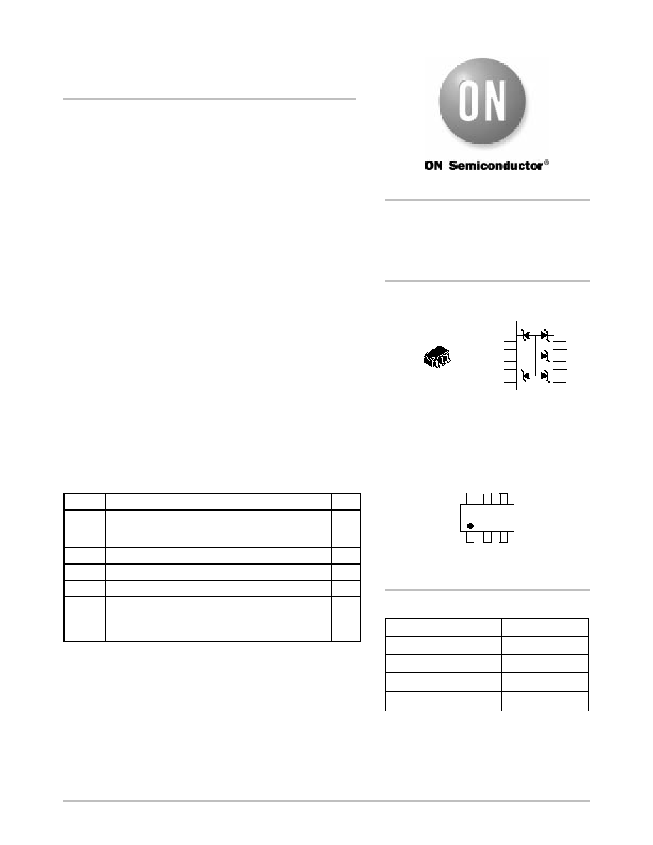
SC-74 FIVE TRANSIENT
VOLTAGE SUPPRESSOR
350 W PEAK POWER
SC-74
CASE 318F
STYLE 6
1
2
3
6
5
4
MARKING DIAGRAM
PIN ASSIGNMENT
Device
Package
Shipping
ORDERING INFORMATION
SMS05CT1
SC-74
3000/Tape & Reel
PIN 1. CATHODE
2. ANODE
3. CATHODE
4. CATHODE
5. CATHODE
6. CATHODE
http://onsemi.com
1
6
DEV
M
DEV
= Specific Device Code
M
= Date Code
SMS12CT1
SC-74
3000/Tape & Reel
SMS15CT1
SC-74
3000/Tape & Reel
SMS24CT1
SC-74
3000/Tape & Reel
SMS05C, SMS12C, SMS15C, SMS24C
http://onsemi.com
2
SMS05C ELECTRICAL CHARACTERISTICS
(T
J
=25
°
C unless otherwise specified)
Parameter
Symbol
Conditions
Min
Typ
Max
Unit
Reverse Working Voltage
V
RWM
(Note 2)
5.0
V
Breakdown Voltage
V
BR
I
T
=1 mA, (Note 3)
6.2
7.2
V
Reverse Leakage Current
I
R
V
RWM
= 5 V
5.0
m
A
Clamping Voltage
V
C
I
PP
= 5 A (8x20
m
s Waveform)
9.8
V
Clamping Voltage
V
C
I
PP
= 24 A (8x20
m
s Waveform)
14.5
V
Maximum Peak Pulse Current
I
PP
8x20
m
s Waveform
24
A
Capacitance
C
J
V
R
= 0 V, f=1 MHz (Line to GND)
260
400
pF
SMS12C ELECTRICAL CHARACTERISTICS
(T
J
=25
°
C unless otherwise specified)
Parameter
Symbol
Conditions
Min
Typ
Max
Unit
Reverse Working Voltage
V
RWM
(Note 2)
12
V
Breakdown Voltage
V
BR
I
T
=1 mA, (Note 3)
13.3
15
V
Reverse Leakage Current
I
R
V
RWM
= 12 V
0.001
1.0
m
A
Clamping Voltage
V
C
I
PP
= 5 A (8x20
m
s Waveform)
19
V
Clamping Voltage
V
C
I
PP
= 15 A (8x20
m
s Waveform)
23
V
Maximum Peak Pulse Current
I
PP
8x20
m
s Waveform
15
A
Capacitance
C
J
V
R
= 0 V, f=1 MHz (Line to GND)
120
150
pF
SMS15C ELECTRICAL CHARACTERISTICS
(T
J
=25
°
C, unless otherwise specified)
Parameter
Symbol
Conditions
Min
Typ
Max
Unit
Reverse Working Voltage
V
RWM
(Note 2)
15
V
Breakdown Voltage
V
BR
I
T
=1 mA, (Note 3)
17
19
V
Reverse Leakage Current
I
R
V
RWM
= 15 V
0.05
1.0
m
A
Clamping Voltage
V
C
I
PP
= 5 A (8x20
m
s Waveform)
24
V
Clamping Voltage
V
C
I
PP
= 12 A (8x20
m
s Waveform)
29
V
Maximum Peak Pulse Current
I
PP
8x20
m
s Waveform
12
A
Capacitance
C
J
V
R
= 0 V, f=1 MHz (Line to GND)
95
125
pF
SMS24C ELECTRICAL CHARACTERISTICS
(T
J
=25
°
C, unless otherwise specified)
Parameter
Symbol
Conditions
Min
Typ
Max
Unit
Reverse Working Voltage
V
RWM
(Note 2)
24
V
Breakdown Voltage
V
BR
I
T
=1 mA, (Note 3)
26.7
32
V
Reverse Leakage Current
I
R
V
RWM
= 24 V
0.001
1.0
m
A
Clamping Voltage
V
C
I
PP
= 5 A (8x20
m
s Waveform)
40
V
Clamping Voltage
V
C
I
PP
= 8 A (8x20
m
s Waveform)
44
V
Maximum Peak Pulse Current
I
PP
8x20
m
s Waveform
8.0
A
Capacitance
C
J
V
R
= 0 V, f=1 MHz (Line to GND)
60
75
pF
2. Note 2. TVS devices are normally selected according to the working peak reverse voltage (V
RWM
), which should be equal or greater than
the DC or continuous peak operating voltage level.
3. Note 3. V
BR
is measured at pulse test current I
T
.
SMS05C, SMS12C, SMS15C, SMS24C
http://onsemi.com
3
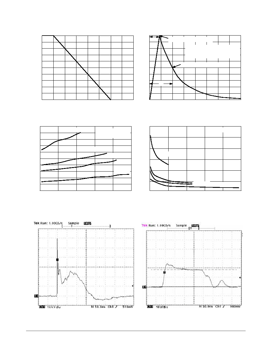
TYPICAL PERFORMANCE CURVES
(T
J
=25
°
C unless otherwise specified)
Figure 1. Pulse Derating Curve
100
90
80
70
60
50
40
30
20
10
0
0
25
50
75
100
125
150
175
200
T
A
, AMBIENT TEMPERATURE (
°
C)
PEAK PULSE DERA
TING IN % OF PEAK POWER
OR CURRENT
@
T A
= 25
C
°
Figure 2. 8
×
20
m
s Pulse Waveform
100
90
80
70
60
50
40
30
20
10
0
0
20
40
60
t, TIME (
m
s)
% OF PEAK PULSE CURRENT
t
P
t
r
PULSE WIDTH (t
P
) IS DEFINED
AS THAT POINT WHERE THE
PEAK CURRENT DECAY = 8
m
s
PEAK VALUE I
RSM
@ 8
m
s
HALF VALUE I
RSM
/2 @ 20
m
s
80
Figure 3. Clamping Voltage vs Peak Pulse Current
50
30
25
20
15
10
5
0
0
5
10
I
PP
, PEAK PULSE CURRENT (A)
V
C
, CLAMPING VOL
T
AGE (V)
15
20
25
Figure 4. Junction Capacitance vs Reverse Voltage
300
250
200
150
100
50
0
0
5
V
BR
, REVERSE VOLTAGE (V)
JUNCTION CAP
ACIT
ANCE (pF)
10
15
20
25
45
40
35
8 x 20
m
s
PULSE WAVEFORM
f = 1.0 MHz
SMS05C
SMS12C
SMS15C
SMS24C
SMS05C
SMS12C
SMS15C
SMS24C
Figure 5. ESD Pulse IEC 61000-4-2
(8 kV Contact)
Figure 6. SMS15CT1 ESD Response for IEC
61000-4-2 (+8 kV Contact)
SMS05C, SMS12C, SMS15C, SMS24C
http://onsemi.com
4
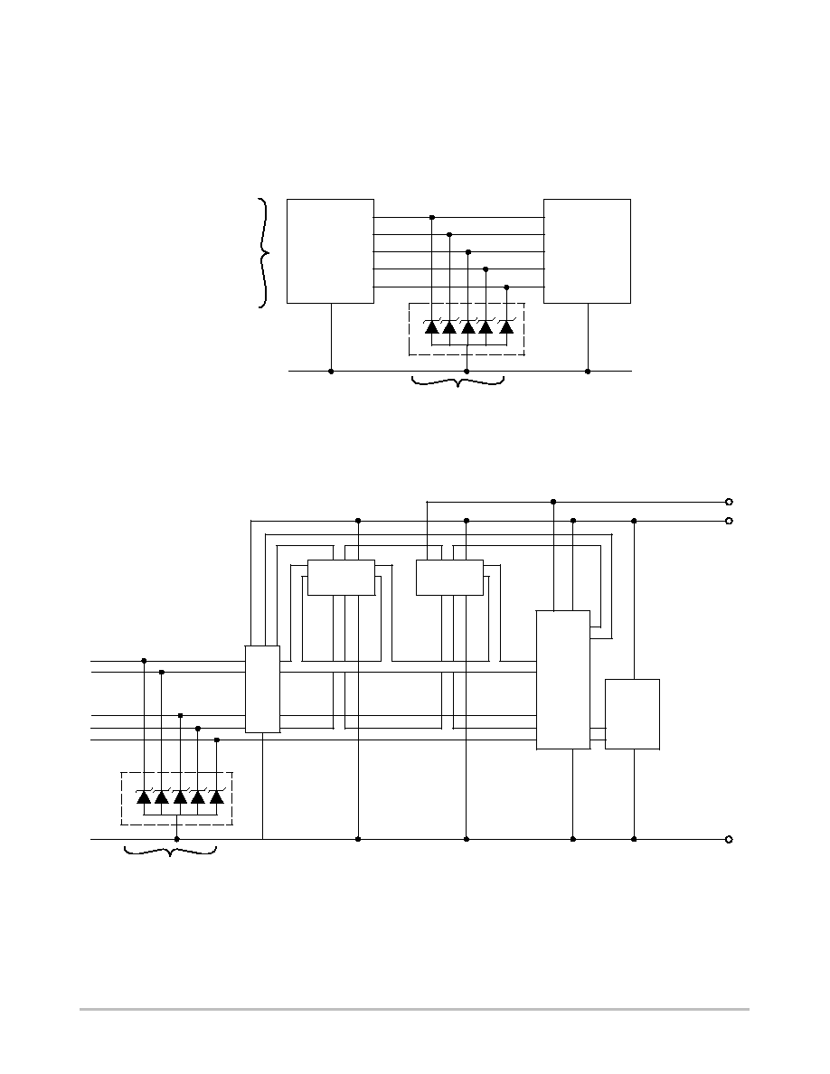
TYPICAL COMMON ANODE APPLICATIONS
A 5 TVS junction common anode design in a SC-74
package protects four separate lines using only one package.
This adds flexibility and creativity to PCB design especially
when board space is at a premium. A simplified example of
SMS05C Series Device applications is illustrated below.
KEYBOARD
TERMINAL
PRINTER
ETC.
FUNCTIONAL
DECODER
I/O
A
SMS05C SERIES DEVICE
GND
Computer Interface Protection
B
C
D
Microprocessor Protection
RAM
ROM
CLOCK
CPU
CONTROL BUS
ADDRESS BUS
DATA BUS
GND
V
GG
V
DD
SMS05C SERIES DEVICE
E
I/O
SMS05C, SMS12C, SMS15C, SMS24C
http://onsemi.com
5
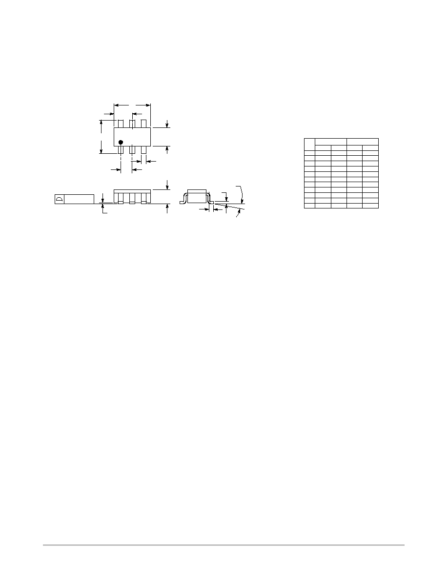
PACKAGE DIMENSIONS
SC-74
CASE 318F-04
ISSUE K
2
3
4
5
6
A
L
1
S
G
D
B
H
C
0.05 (0.002)
DIM
MIN
MAX
MIN
MAX
MILLIMETERS
INCHES
A 0.1142 0.1220
2.90
3.10
B 0.0512 0.0669
1.30
1.70
C 0.0354 0.0433
0.90
1.10
D 0.0098 0.0197
0.25
0.50
G 0.0335 0.0413
0.85
1.05
H 0.0005 0.0040
0.013
0.100
J 0.0040 0.0102
0.10
0.26
K 0.0079 0.0236
0.20
0.60
L 0.0493 0.0649
1.25
1.65
M
0
10
0
10
S 0.0985 0.1181
2.50
3.00
_
_
_
_
NOTES:
1. DIMENSIONING AND TOLERANCING
PER ANSI Y14.5M, 1982.
2. CONTROLLING DIMENSION: INCH.
3. MAXIMUM LEAD THICKNESS INCLUDES
LEAD FINISH THICKNESS. MINIMUM
LEAD THICKNESS IS THE MINIMUM
THICKNESS OF BASE MATERIAL.
4. 318F-01, -02, -03 OBSOLETE. NEW
STANDARD 318F-04.
M
J
K
STYLE 6:
PIN 1. CATHODE
2. ANODE
3. CATHODE
4. CATHODE
5. CATHODE
6. CATHODE