 | –≠–ª–µ–∫—Ç—Ä–æ–Ω–Ω—ã–π –∫–æ–º–ø–æ–Ω–µ–Ω—Ç: SS24T3 | –°–∫–∞—á–∞—Ç—å:  PDF PDF  ZIP ZIP |

©
Semiconductor Components Industries, LLC, 2005
July, 2005 - Rev. 2
1
Publication Order Number:
SS24/D
SS22, SS24
Surface Mount
Schottky Power Rectifier
SMB Power Surface Mount Package
These devices employ the Schottky Barrier principle in a
metal-to-silicon power rectifier. Features epitaxial construction with
oxide passivation and metal overlay contact. Ideally suited for low
voltage, high frequency switching power supplies; free wheeling
diodes and polarity protection diodes.
Features
∑
Compact Package with J-Bend Leads Ideal for Automated Handling
∑
Highly Stable Oxide Passivated Junction
∑
Guardring for Over-Voltage Protection
∑
Low Forward Voltage Drop
∑
Pb-Free Package is Available
Mechanical Characteristics
∑
Case: Molded Epoxy
∑
Epoxy Meets UL 94 V-0 @ 0.125 in
∑
Weight: 95 mg (approximately)
∑
Cathode Polarity Band
∑
Lead and Mounting Surface Temperature for Soldering Purposes:
260
∞C Max. for 10 Seconds
∑
Available in 12 mm Tape, 2500 Units per 13 in Reel, Add "T3"
Suffix to Part Number
∑
Finish: All External Surfaces Corrosion Resistant and Terminal
Leads are Readily Solderable
∑
ESD Ratings: Machine Model = C
ESD Ratings:
Human Body Model = 3B
SMB
CASE 403A
PLASTIC
SCHOTTKY BARRIER
RECTIFIER
2 AMPERES
20, 40 VOLTS
http://onsemi.com
SS2x
= Specific Device Code
x
= 2 or 4
A
= Assembly Location
Y
= Year
WW
= Work Week
G
= Pb-Free Package
(Note: Microdot may be in either location)
AYWW
SS2x
G
G
Device
Package
Shipping
ORDERING INFORMATION
SS22T3
SMB
2500/Tape & Reel
MARKING DIAGRAM
SS24T3
SMB
2500/Tape & Reel
For information on tape and reel specifications,
including part orientation and tape sizes, please
refer to our Tape and Reel Packaging Specifications
Brochure, BRD8011/D.
SS24T3G
SMB
(Pb-Free)
2500/Tape & Reel

SS22, SS24
http://onsemi.com
2
MAXIMUM RATINGS
Rating
Symbol
Value
Unit
Peak Repetitive Reverse Voltage
Working Peak Reverse Voltage
DC Blocking Voltage
SS22
SS24
V
RRM
V
RWM
V
R
20
40
V
Average Rectified Forward Current
(At Rated V
R
, T
L
= 100
∞
C)
I
O
2.0
A
Peak Repetitive Forward Current
(At Rated V
R
, Square Wave,
100 kHz, T
C
= 105
∞
C)
I
FRM
3.0
A
Non-Repetitive Peak Surge Current
(Surge Applied at Rated Load Conditions Halfwave, Single Phase, 60 Hz)
I
FSM
75
A
Storage/Operating Case Temperature
T
stg
, T
C
-55 to +150
∞
C
Operating Junction Temperature
T
J
-55 to +125
∞
C
Voltage Rate of Change
(Rated V
R
, T
J
= 25
∞
C)
dv/dt
10,000
V/
m
s
Maximum ratings are those values beyond which device damage can occur. Maximum ratings applied to the device are individual stress limit
values (not normal operating conditions) and are not valid simultaneously. If these limits are exceeded, device functional operation is not implied,
damage may occur and reliability may be affected.
THERMAL CHARACTERISTICS
Characteristic
Symbol
Value
Unit
Thermal Resistance,
Junction-to-Lead (Note 1)
Thermal Resistance,
Junction-to-Ambient (Note 2)
R
q
JL
R
q
JA
24
80
∞
C/W
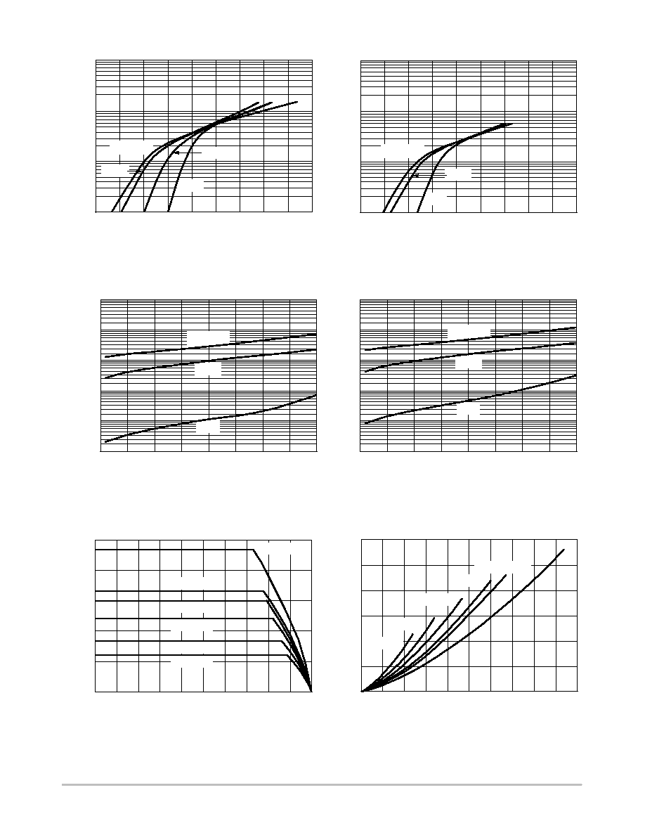
ELECTRICAL CHARACTERISTICS
Maximum Instantaneous Forward Voltage
(Note 3)
see Figure 2
(i
F
= 2.0 A)
v
F
T
J
= 25
∞
C
T
J
= 125
∞
C
V
0.50
0.46
Maximum Instantaneous Reverse Current (Note 3)
see Figure 4
(V
R
= 40 V)
I
R
T
J
= 25
∞
C
T
J
= 100
∞
C
mA
0.4
5.7
1. Mounted with minimum recommended pad size, PC Board FR4.
2. 1 inch square pad size (1 x 0.5 inch for each lead) on FR4 board.
3. Pulse Test: Pulse Width
250
m
s, Duty Cycle
2.0%.
SS22, SS24
http://onsemi.com
3
Figure 1. Typical Forward Voltage
Figure 2. Maximum Forward Voltage
Figure 3. Typical Reverse Current
Figure 4. Maximum Reverse Current
Figure 5. Current Derating
Figure 6. Forward Power Dissipation
0.7
0.1
v
F
, INSTANTANEOUS FORWARD VOLTAGE (VOLTS)
10
1.0
40
0
V
R
, REVERSE VOLTAGE (VOLTS)
100E-3
10E-3
1.0E-3
100E-6
10E-6
1.0E-6
45
85
25
T
L
, LEAD TEMPERATURE (∞C)
2.5
1.5
1.0
0.5
0
I
O
, AVERAGE FORWARD CURRENT (AMPS)
0.5
2.0
0
1.2
1.0
0.8
0.6
0.2
0
65
i F
, INST
ANT
ANEOUS
FOR
W
ARD
CURRENT
(AMPS)
I
0.1
0.3
0.5
0.9
10
20
30
, A
VERAGE
FOR
W
ARD
CURRENT
(AMPS)
I O
125
105
1.0
2.5
1.5
0.4
P
FO
,
A
VERAGE POWER DISSIP
A
TION
(W
A
TTS)
100
T
J
= 125∞C
100∞C
25∞C
-40 ∞C
0.7
0.1
V
F
, MAXIMUM INSTANTANEOUS FORWARD VOLTAGE (VOLTS)
10
1.0
I F
, INST
ANT
ANEOUS
FOR
W
ARD
CURRENT
(AMPS)
0.1
0.3
0.5
0.9
100
T
J
= 125∞C
100∞C
25∞C
, REVERSE CURRENT
(AMPS)
R
40
0
V
R
, REVERSE VOLTAGE (VOLTS)
100E-3
10E-3
1.0E-3
100E-6
10E-6
1.0E-6
I
10
20
30
, MAXIMUM REVERSE CURRENT
(AMPS)
R
2.0
FREQ = 20 kHz
T
J
= 125∞C
100∞C
25∞C
T
J
= 125∞C
100∞C
25∞C
dc
SQUARE WAVE
Ipk/Io = p
Ipk/Io = 5.0
Ipk/Io = 10
Ipk/Io = 20
dc
SQUARE WAVE
Ipk/Io = p
Ipk/Io = 5.0
Ipk/Io = 10
Ipk/Io = 20

SS22, SS24
http://onsemi.com
4
Figure 7. Capacitance
Figure 8. Typical Operating Temperature Derating*
Figure 9. Thermal Response -- Junction to Case
Figure 10. Thermal Response -- Junction to Ambient
30
0
V
R
, REVERSE VOLTAGE (VOLTS)
1000
100
10
V
R
, DC REVERSE VOLTAGE (VOLTS)
25
40
0
105
85
75
65
C, CAP
ACIT
ANCE
(pF)
T
15
5.0
10
20
25
35
40
30
35
5.0
10
20
15
95
115
125
,
DERA
TED
OPERA
TING TEMPERATURE ( C)
J
∞
* Reverse power dissipation and the possibility of thermal runaway must be considered when operating this device under any re-
verse voltage conditions. Calculations of T
J
therefore must include forward and reverse power effects. The allowable operating
T
J
may be calculated from the equation:
T
J
= T
Jmax
- r(t)(Pf + Pr) where
r(t) = thermal impedance under given conditions,
Pf = forward power dissipation, and
Pr = reverse power dissipation
This graph displays the derated allowable T
J
due to reverse bias under DC conditions only and is calculated as T
J
= T
Jmax
- r(t)Pr,
where r(t) = Rthja. For other power applications further calculations must be performed.
R
tja
= 24∞C/W
43∞C/W
63∞C/W
80∞C/W
93∞C/W
T
J
= 25∞C
0.1
0.00001
t, TIME (s)
1.0E+00
1.0E-01
1.0E-02
1.0E-03
1.0E-04
R
0.0001
0.001
0.01
, TRANSIENT
THERMAL
RESIST
ANCE
(NORMALIZED)
T
1.0
10
100
1000
50%
20%
10%
5.0%
2.0%
1.0%
R
tjl(t)
= R
tjl*r(t)
0.1
0.00001
t, TIME (s)
1.0E+00
1.0E-01
1.0E-02
1.0E-03
1.0E-04
0.0001
0.001
0.01
1.0
10
100
1000
50%
20%
10%
5.0%
2.0%
1.0%
R
tjl(t)
= R
tjl*r(t)
R
,
TRANSIENT
THERMAL
RESIST
ANCE
(NORMALIZED)
T
SS22, SS24
http://onsemi.com
5
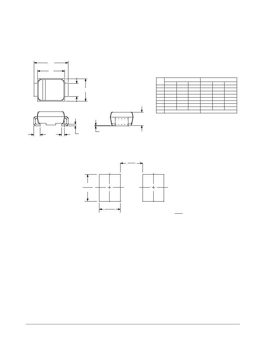
PACKAGE DIMENSIONS
SMB
CASE 403A-03
ISSUE E
2.261
0.089
2.743
0.108
2.159
0.085
mm
inches
SCALE 8:1
*For additional information on our Pb-Free strategy and soldering
details, please download the ON Semiconductor Soldering and
Mounting Techniques Reference Manual, SOLDERRM/D.
SOLDERING FOOTPRINT*
E
b
D
c
L1
L
A
A1
NOTES:
1. DIMENSIONING AND TOLERANCING PER ANSI Y14.5M, 1982.
2. CONTROLLING DIMENSION: INCH.
3. D DIMENSION SHALL BE MEASURED WITHIN DIMENSION P.
DIM
A
MIN
NOM
MAX
MIN
MILLIMETERS
1.90
2.13
2.41
0.075
INCHES
A1
0.05
0.10
0.15
0.002
b
1.96
2.03
2.11
0.077
c
0.15
0.23
0.30
0.006
D
3.30
3.56
3.81
0.130
E
4.06
4.32
4.57
0.160
L
0.76
1.02
1.27
0.030
0.084
0.095
0.004
0.006
0.080
0.083
0.009
0.012
0.140
0.150
0.170
0.180
0.040
0.050
NOM
MAX
5.21
5.44
5.59
0.205
0.214
0.220
H
E
0.51 REF
0.020 REF
D
L1
H
E