 | –≠–ª–µ–∫—Ç—Ä–æ–Ω–Ω—ã–π –∫–æ–º–ø–æ–Ω–µ–Ω—Ç: TBD | –°–∫–∞—á–∞—Ç—å:  PDF PDF  ZIP ZIP |
©
Semiconductor Components Industries, LLC, 2003
November, 2003 - Rev. P0
1
Publication Order Number:
NCP1225/D
NCP1225
Product Preview
Low Standby Power
SMPS Controller
NCP1225 is a low standby power Switch-Mode Power Supply,
SMPS controller IC specially designed for low power AC-DC
adapter applications. The device operates in Discontinuous
Conduction Mode (DCM) with Pulse Frequency Modulation (PFM)
control scheme. PFM operation can provide high operating
efficiency even at light loading conditions and the device itself takes
extremely low operating current. With careful circuit design, low
standby power down to 300 mW can be achieved for universal line
input low power adapters. This specific feature can help the end
products to comply with immediate and future international power
saving regulations easily.
An innovative feedback compensation scheme is integrated in
NCP1225 to eliminate the expensive optocoupler in the feedback
path. By only using simple auxiliary winding feedback, the regulator
still can achieve good output voltage regulation usually not possible
with common SMPS controller ICs without optocoupler. For even
better regulation applications, optocoupler feedback can still be used
in place. Additionally, value-added features as overvoltage
protection, undervoltage lockout and overcurrent protection
functions are also included. This controller is an ideal solution for
low power adapters and mobile phone chargers. With all valuable
features, this device is available in the tiny TSOP-5 package.
Features
∑
Current Mode Operation
∑
Cycle-By-Cycle Current Limiting
∑
High Efficiency Pulse Frequency Modulation (PFM) Control
∑
Low Device Operating Current, 0.5 mA Typical
∑
No Optocoupler Feedback Control
∑
Extremely Low Standby Power
∑
Internal Leading Edge Blanking
∑
Input Undervoltage Lockout Protection
∑
Output Overvoltage Protection
∑
Optional Optocoupler Feedback
∑
Micro Miniature TSOP-5 Package
Typical Applications
∑
Low Power Wall Mount Adapters
∑
Mobile Phone Adapter Chargers
∑
TV/Computer Auxiliary Power Supply
This document contains information on a product under development. ON Semiconductor
reserves the right to change or discontinue this product without notice.
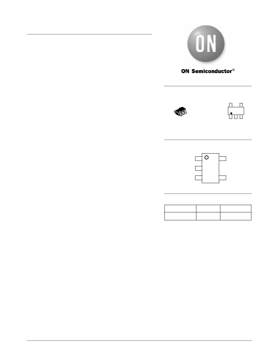
TSOP-5
SN SUFFIX
CASE 483
PIN CONNECTIONS
Device
Package
Shipping
ORDERING INFORMATION
TBD
TSOP-5
TBD
http://onsemi.com
TBD = Device Code
M
= Date Code
MARKING
DIAGRAM
1
5
1
5
TBD
M
1
3
CS
V
CC
2
GND
VDRIVE
4
GATE
5
(Top View)

NCP1225
http://onsemi.com
2
V
CC
+
-
+
-
7.5/12 V
Reference
0.125 V
S
R
Q
Q
OR
AND
VDRIVE
GATE
+
-
1 V
+
-
0.5 V
TON MAX
GND
LEB
CS
Figure 1. Simple Block Diagram
+
-
+
-
+
-
+
-

NCP1225
http://onsemi.com
3
PIN FUNCTION DESCRIPTION
Pin
Symbol
Description
1
V
CC
This pin is the supply of the IC. When voltage at this pin is higher than 12 V typical, the operation will
be activated.
2
GND
This pin is the ground of the primary side of the system.
3
VDRIVE
This pin is also used to detect the current status of secondary winding.
4
CS
The Current Sense pin senses the voltage developed across the current sensing resistor in series with
the power MOSFET. This information is used to terminate the output switch conduction cycle.
5
GATE
Controller output to the gate of the power MOSFET.
MAXIMUM RATINGS
Rating
Symbol
Value
Unit
Supply Voltage, V
CC
V
CC
-0.3 to 16
V
Gate Output Current, Source Current (Note 1)
I
O_SRC
350
mA
Gate Output Current, Sink Current (Note 1)
I
O_SINK
450
mA
Thermal Characteristics
TSOP-5 Plastic Package, Case 483
Thermal Resistance, Junction-to-Air
R
q
JA
250
∞
C/W
Current Sense, CS Input Voltage
V
CS
-0.3 to 10
V
VDRIVE Input Voltage
V
DRIVE
-0.3 to 10
V
Gate Voltage
V
GATE
-0.3 to 16
V
Operating Junction Temperature
T
J
-25 to +150
∞
C
Operating Ambient Temperature
T
A
-25 to +105
∞
C
Storage Temperature Range
T
stg
-65 to 150
∞
C
ESD Capability, HBM Model
-
2.0
KV
ESD Capability, Machine Model
-
200
V
1. Maximum package power dissipation limits must be observed.

NCP1225
http://onsemi.com
4
ELECTRICAL CHARACTERISTICS
(For typical values
V
CC
= 13 V, T
A
= 25
∞
C, and for min/max values T
A
= -25
∞
C to +105
∞
C, unless otherwise noted.)
Characteristic
Symbol
Min
Typ
Max
Unit
CURRENT SENSE COMPARATOR (PIN 4)
Current Sense Reset Threshold
V
CS_RESET
0.95
1.0
1.05
V
Current Sense Set Threshold
V
CS_SET
0.475
0.5
0.525
V
Input Bias Current
I
IB
-
TBD
-
m
A
Propagation Delay (Current Sense Input to Output)
t
PLH
-
200
-
ns
VDRIVE (PIN 3)
Vdrive Sense Pin Threshold
V
DRIVE_SET_TH
0.118
0.125
0.131
V
Input Bias Current
I
VDRIVE_IB
-
50
-
nA
GATE (PIN 5)
Output Voltage Rise Time (C
L
= 1.0 nF, T
A
= 25
∞
C)
t
R
-
55
-
ns
Output Voltage Fall Time (C
L
= 1.0 nF, T
A
= 25
∞
C)
t
F
-
40
-
ns
Output Voltage
Low State (Isink = 20 mA)
(Isink = 100 mA)
V
OL
-
-
0.27
1.5
-
-
V
High State (Isource = 20 mA)
(Isource = 100 mA)
V
OH
-
-
11.7
10
-
-
V
Gate Signal Maximum ON Time
T
ON(MAX)
8.0
10
12
m
s
UNDERVOLTAGE LOCKOUT (PIN 1)
Start-Up Threshold (V
CC
Rising)
V
TH(ON)
11
12
13
V
Minimum Operation Voltage After Turn-On
V
CC(MIN)
6.5
7.5
8.5
V
OVERVOLTAGE PROTECTION (PIN 1)
Overvoltage Protect (OVP) Threshold
V
TH(OVP)
13.5
14.5
15.5
V
TOTAL DEVICE
Power Supply Current Startup (V
CC
= 10 V)
I
START
-
-
60
m
A
Operating Current (No Switch, T
A
= 25
∞
C)
I
CC
-
0.5
-
mA

NCP1225
http://onsemi.com
5
90
X
264 Vac
4.7
m
F x 2
2 Meg
4.7
m
F
200 K
1
3
CS
V
CC
2
GND
VDRIVE
4
GATE
5
200 K
NCP1225
4.7
m
F
100 K
47 n
500
470
m
F
MUR1100
1N4007
3
1N60E
Figure 2. Typical Application Circuit Without Optocoupler

NCP1225
http://onsemi.com
6
PACKAGE DIMENSIONS
TSOP-5
SN SUFFIX
CASE 483-02
ISSUE C
NOTES:
1. DIMENSIONING AND TOLERANCING PER ANSI
Y14.5M, 1982.
2. CONTROLLING DIMENSION: MILLIMETER.
3. MAXIMUM LEAD THICKNESS INCLUDES LEAD
FINISH THICKNESS. MINIMUM LEAD THICKNESS
IS THE MINIMUM THICKNESS OF BASE
MATERIAL.
DIM
MIN
MAX
MIN
MAX
INCHES
MILLIMETERS
A
2.90
3.10 0.1142 0.1220
B
1.30
1.70 0.0512 0.0669
C
0.90
1.10 0.0354 0.0433
D
0.25
0.50 0.0098 0.0197
G
0.85
1.05 0.0335 0.0413
H
0.013
0.100 0.0005 0.0040
J
0.10
0.26 0.0040 0.0102
K
0.20
0.60 0.0079 0.0236
L
1.25
1.55 0.0493 0.0610
M
0
10
0
10
S
2.50
3.00 0.0985 0.1181
0.05 (0.002)
1
2
3
5
4
S
A
G
L
B
D
H
C
K
M
J
_
_
_
_
ON Semiconductor and are registered trademarks of Semiconductor Components Industries, LLC (SCILLC). SCILLC reserves the right to make changes without further notice
to any products herein. SCILLC makes no warranty, representation or guarantee regarding the suitability of its products for any particular purpose, nor does SCILLC assume any
liability arising out of the application or use of any product or circuit, and specifically disclaims any and all liability, including without limitation special, consequential or incidental
damages. "Typical" parameters which may be provided in SCILLC data sheets and/or specifications can and do vary in different applications and actual performance may vary over
time. All operating parameters, including "Typicals" must be validated for each customer application by customer's technical experts. SCILLC does not convey any license under
its patent rights nor the rights of others. SCILLC products are not designed, intended, or authorized for use as components in systems intended for surgical implant into the body,
or other applications intended to support or sustain life, or for any other application in which the failure of the SCILLC product could create a situation where personal injury or death
may occur. Should Buyer purchase or use SCILLC products for any such unintended or unauthorized application, Buyer shall indemnify and hold SCILLC and its officers, employees,
subsidiaries, affiliates, and distributors harmless against all claims, costs, damages, and expenses, and reasonable attorney fees arising out of, directly or indirectly, any claim of
personal injury or death associated with such unintended or unauthorized use, even if such claim alleges that SCILLC was negligent regarding the design or manufacture of the part.
SCILLC is an Equal Opportunity/Affirmative Action Employer. This literature is subject to all applicable copyright laws and is not for resale in any manner.
PUBLICATION ORDERING INFORMATION
N. American Technical Support: 800-282-9855 Toll Free
USA/Canada
Japan: ON Semiconductor, Japan Customer Focus Center
2-9-1 Kamimeguro, Meguro-ku, Tokyo, Japan 153-0051
Phone: 81-3-5773-3850
NCP1225/D
LITERATURE FULFILLMENT:
Literature Distribution Center for ON Semiconductor
P.O. Box 5163, Denver, Colorado 80217 USA
Phone: 303-675-2175 or 800-344-3860 Toll Free USA/Canada
Fax: 303-675-2176 or 800-344-3867 Toll Free USA/Canada
Email: orderlit@onsemi.com
ON Semiconductor Website: http://onsemi.com
Order Literature: http://www.onsemi.com/litorder
For additional information, please contact your
local Sales Representative.