 | –≠–ª–µ–∫—Ç—Ä–æ–Ω–Ω—ã–π –∫–æ–º–ø–æ–Ω–µ–Ω—Ç: VN2222LL | –°–∫–∞—á–∞—Ç—å:  PDF PDF  ZIP ZIP |

©
Semiconductor Components Industries, LLC, 2004
September, 2004 - Rev. 3
1
Publication Order Number:
VN2222LL/D
VN2222LL
Preferred Device
Small Signal MOSFET
150 mAmps, 60 Volts
N-Channel TO-92
Features
∑
Pb-Free Packages are Available*
MAXIMUM RATINGS
Rating
Symbol
Value
Unit
Drain - Source Voltage
V
DSS
60
Vdc
Drain-Gate Voltage (R
GS
= 1.0 M
W
)
V
DGR
60
Vdc
Gate-Source Voltage
- Continuous
- Non-repetitive (t
p
50
m
s)
V
GS
V
GSM
±
20
±
40
Vdc
Vpk
Drain Current
- Continuous
- Pulsed
I
D
I
DM
150
1000
mAdc
Total Power Dissipation @ T
A
= 25
∞
C
Derate above 25
∞
C
P
D
400
3.2
mW
mW/
∞
C
Operating and Storage Temperature Range
T
J
, T
stg
- 55 to
+150
∞
C
Maximum ratings are those values beyond which device damage can occur.
Maximum ratings applied to the device are individual stress limit values (not
normal operating conditions) and are not valid simultaneously. If these limits
are exceeded, device functional operation is not implied, damage may occur
and reliability may be affected.
THERMAL CHARACTERISTICS
Characteristic
Symbol
Max
Unit
Thermal Resistance, Junction-to-Ambient
R
q
JA
312.5
∞
C/W
Maximum Lead Temperature for
Soldering Purposes, 1/16
from case
for 10 seconds
T
L
300
∞
C
*For additional information on our Pb-Free strategy and soldering details, please
download the ON Semiconductor Soldering and Mounting Techniques
Reference Manual, SOLDERRM/D.
VN22
22LL
AYWW
D
G
TO-92
CASE 29
STYLE 22
N-Channel
S
1 2
3
1
Source
3
Drain
2
Gate
150 mA, 60 V
R
DS(on)
= 7.5
W
Preferred devices are recommended choices for future use
and best overall value.
See detailed ordering and shipping information in the package
dimensions section on page 2 of this data sheet.
ORDERING INFORMATION
A
= Assembly Location
Y
= Year
WW
= Work Week
MARKING DIAGRAM
& PIN ASSIGNMENT
http://onsemi.com

VN2222LL
http://onsemi.com
2
ELECTRICAL CHARACTERISTICS
(T
C
= 25
∞
C unless otherwise noted)
Characteristic
Symbol
Min
Max
Unit
OFF CHARACTERISTICS
Drain-Source Breakdown Voltage
(V
GS
= 0, I
D
= 100
m
Adc)
V
(BR)DSS
60
-
Vdc
Zero Gate Voltage Drain Current
(V
DS
= 48 Vdc, V
GS
= 0)
(V
DS
= 48 Vdc, V
GS
= 0, T
J
= 125
∞
C)
I
DSS
-
-
10
500
m
Adc
Gate-Body Leakage Current, Forward
(V
GSF
= 30 Vdc, V
DS
= 0)
I
GSSF
-
-100
nAdc
ON CHARACTERISTICS (Note 1)
Gate Threshold Voltage
(V
DS
= V
GS
, I
D
= 1.0 mAdc)
V
GS(th)
0.6
2.5
Vdc
Static Drain-Source On-Resistance
(V
GS
= 10 Vdc, I
D
= 0.5 Adc)
(V
GS
= 10 Vdc, I
D
= 0.5 Vdc, T
C
= 125
∞
C)
r
DS(on)
-
-
7.5
13.5
W
Drain-Source On-Voltage
(V
GS
= 5.0 Vdc, I
D
= 200 mAdc)
(V
GS
= 10 Vdc, I
D
= 500 mAdc)
V
DS(on)
-
-
1.5
3.75
Vdc
On-State Drain Current
(V
GS
= 10 Vdc, V
DS
2.0 V
DS(on)
)
I
D(on)
750
-
mA
Forward Transconductance
(V
DS
= 10 Vdc, I
D
= 500 mAdc)
g
fs
100
-
m
mhos
DYNAMIC CHARACTERISTICS
Input Capacitance
(V
25 Vd
V
0
C
iss
-
60
pF
Output Capacitance
(V
DS
= 25 Vdc, V
GS
= 0,
f = 1.0 MHz)
C
oss
-
25
Reverse Transfer Capacitance
f = 1.0 MHz)
C
rss
-
5.0
SWITCHING CHARACTERISTICS (Note 1)
Turn-On Delay Time
(V
DD
= 15 Vdc, I
D
= 600 mA,
t
on
-
10
ns
Turn-Off Delay Time
(V
DD
15 Vdc, I
D
600 mA,
R
gen
= 25
W
, R
L
= 23
W
)
t
off
-
10
1. Pulse Test: Pulse Width
v
300
m
s, Duty Cycle
v
2.0%.
ORDERING INFORMATION
Device
Package
Shipping
VN2222LL
TO-92
1000 Unit / Box
VN2222LLG
TO-92
(Pb-Free)
1000 Unit / Box
VN2222LLRL
TO-92
1000 Unit / Box
VN2222LLRLRA
TO-92
2000 Tape & Reel
VN2222LLRLRAG
TO-92
(Pb-Free)
2000 Tape & Reel
VN2222LLRLRM
TO-92
2000 Unit / Ammo Box
For information on tape and reel specifications, including part orientation and tape sizes, please refer to our Tape and Reel Packaging
Specifications Brochure, BRD8011/D.
VN2222LL
http://onsemi.com
3
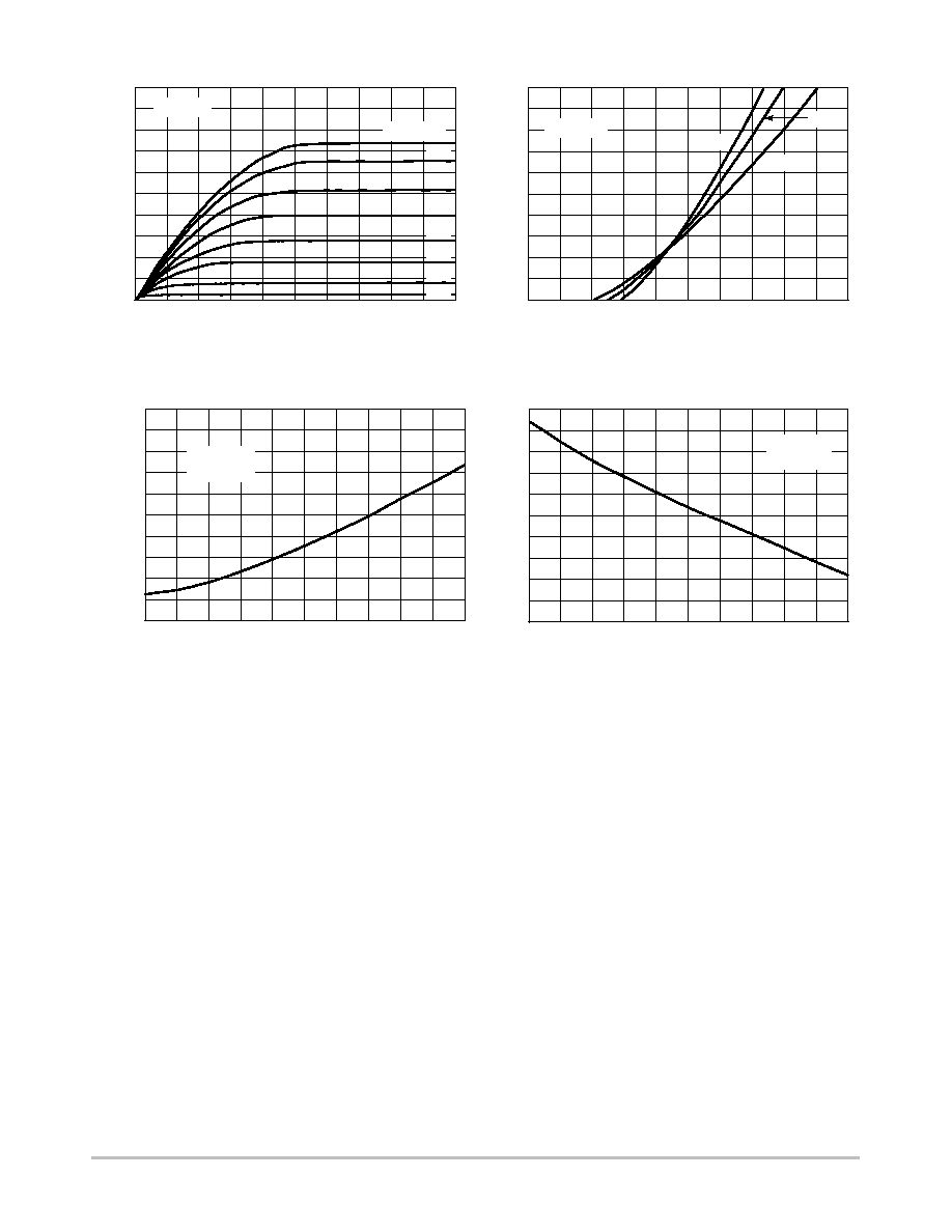
I D
, DRAIN CURRENT
(AMPS)
I D
, DRAIN CURRENT
(AMPS)
V
DS
, DRAIN-SOURCE VOLTAGE (VOLTS)
0.6
0.4
0.2
0.8
1.2
1
0
1
2
3
4
5
1.6
1.4
6
7
8
9
10
Figure 1. Ohmic Region
V
GS
, GATE-SOURCE VOLTAGE (VOLTS)
0
1
2
3
4
5
6
7
8
9
10
1.8
2
0.6
0.4
0.2
0.8
1
T, TEMPERATURE (
∞
C)
T, TEMPERATURE (
∞
C)
0.4
1
0.8
0.6
1.2
1.6
1.4
, ST
A
TIC DRAIN-SOURCE ON-RESIST
ANCE
DS(on)r
-60
-20
+20
2
1.8
+60
+100
+140
2.2
2.4
-60
-20
0
+20
+60
+100
+140
0.7
0.85
0.8
0.75
0.9
1
0.95
1.1
1.05
1.15
1.2
(NORMALIZED)
,
THRESHOLD VOL
T
AGE (NORMALIZED)
GS(th)V
Figure 2. Transfer Characteristics
Figure 3. Temperature versus Static
Drain-Source On-Resistance
Figure 4. Temperature versus Gate
Threshold Voltage
T
A
= 25
∞
C
V
GS
= 10 V
9 V
8 V
7 V
6 V
5 V
4 V
3 V
V
DS
= 10 V
25
∞
C
125
∞
C
-55
∞
C
V
GS
= 10 V
I
D
= 200 mA
V
DS
= V
GS
I
D
= 1 mA
VN2222LL
http://onsemi.com
4
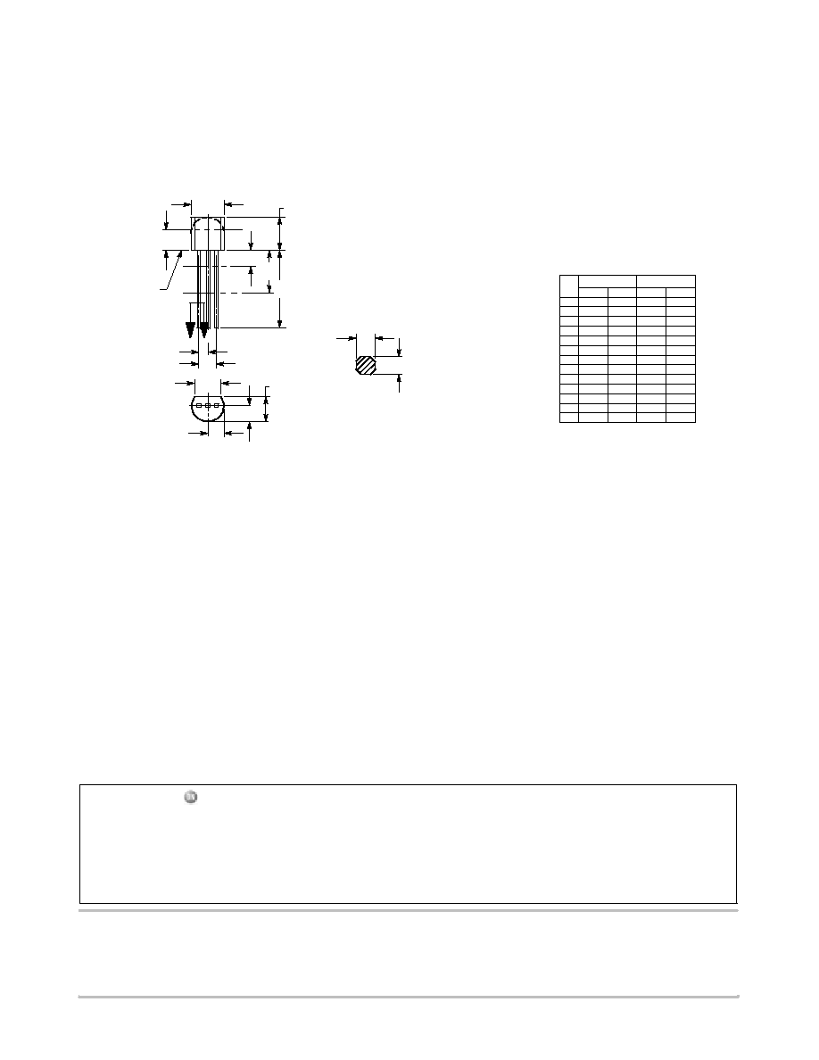
PACKAGE DIMENSIONS
STYLE 22:
PIN 1. SOURCE
2. GATE
3. DRAIN
NOTES:
1. DIMENSIONING AND TOLERANCING PER ANSI
Y14.5M, 1982.
2. CONTROLLING DIMENSION: INCH.
3. CONTOUR OF PACKAGE BEYOND DIMENSION R
IS UNCONTROLLED.
4. LEAD DIMENSION IS UNCONTROLLED IN P AND
BEYOND DIMENSION K MINIMUM.
R
A
P
J
L
B
K
G
H
SECTION X-X
C
V
D
N
N
X X
SEATING
PLANE
DIM
MIN
MAX
MIN
MAX
MILLIMETERS
INCHES
A
0.175
0.205
4.45
5.20
B
0.170
0.210
4.32
5.33
C
0.125
0.165
3.18
4.19
D
0.016
0.021
0.407
0.533
G
0.045
0.055
1.15
1.39
H
0.095
0.105
2.42
2.66
J
0.015
0.020
0.39
0.50
K
0.500
---
12.70
---
L
0.250
---
6.35
---
N
0.080
0.105
2.04
2.66
P
---
0.100
---
2.54
R
0.115
---
2.93
---
V
0.135
---
3.43
---
1
TO-92
CASE 29-11
ISSUE AL
ON Semiconductor and are registered trademarks of Semiconductor Components Industries, LLC (SCILLC). SCILLC reserves the right to make changes without further notice
to any products herein. SCILLC makes no warranty, representation or guarantee regarding the suitability of its products for any particular purpose, nor does SCILLC assume any liability
arising out of the application or use of any product or circuit, and specifically disclaims any and all liability, including without limitation special, consequential or incidental damages.
"Typical" parameters which may be provided in SCILLC data sheets and/or specifications can and do vary in different applications and actual performance may vary over time. All
operating parameters, including "Typicals" must be validated for each customer application by customer's technical experts. SCILLC does not convey any license under its patent rights
nor the rights of others. SCILLC products are not designed, intended, or authorized for use as components in systems intended for surgical implant into the body, or other applications
intended to support or sustain life, or for any other application in which the failure of the SCILLC product could create a situation where personal injury or death may occur. Should
Buyer purchase or use SCILLC products for any such unintended or unauthorized application, Buyer shall indemnify and hold SCILLC and its officers, employees, subsidiaries, affiliates,
and distributors harmless against all claims, costs, damages, and expenses, and reasonable attorney fees arising out of, directly or indirectly, any claim of personal injury or death
associated with such unintended or unauthorized use, even if such claim alleges that SCILLC was negligent regarding the design or manufacture of the part. SCILLC is an Equal
Opportunity/Affirmative Action Employer. This literature is subject to all applicable copyright laws and is not for resale in any manner.
PUBLICATION ORDERING INFORMATION
N. American Technical Support: 800-282-9855 Toll Free
USA/Canada
Japan: ON Semiconductor, Japan Customer Focus Center
2-9-1 Kamimeguro, Meguro-ku, Tokyo, Japan 153-0051
Phone: 81-3-5773-3850
VN2222LL/D
LITERATURE FULFILLMENT:
Literature Distribution Center for ON Semiconductor
P.O. Box 61312, Phoenix, Arizona 85082-1312 USA
Phone: 480-829-7710 or 800-344-3860 Toll Free USA/Canada
Fax: 480-829-7709 or 800-344-3867 Toll Free USA/Canada
Email: orderlit@onsemi.com
ON Semiconductor Website: http://onsemi.com
Order Literature: http://www.onsemi.com/litorder
For additional information, please contact your
local Sales Representative.