
F-51452GNFJ-AA (AA) No. 2002-0072
OPTREX CORPORATION
Page 1/16
LCD Module Technical Specification
F-51452GNFJ-AA
Table of Contents
1. General Specifications
.................................................................................................................................. 2
2. Electrical Specifications
............................................................................................................................... 3
3. Optical Specifications
................................................................................................................................... 6
4. I/O Terminal
...................................................................................................................................................... 8
5. Test
................................................................................................................................................................... 10
6. Appearance Standards
............................................................................................................................... 11
7. Code System of Production Lot
............................................................................................................... 14
8. Type Number
.................................................................................................................................................. 14
9. Applying Precautions
.................................................................................................................................. 14
10. Precautions Relating Product Handling
................................................................................................ 15
11. Warranty
........................................................................................................................................................ 16
Checked by (Design Engineering Div.)
Checked by (Quality Assurance Div.)
Approved by (Production Div.)
Prepared by (Production Div.)
Revision History
Rev.
Date
Page
Comment
Type No.
Feb 28, 2002
O P T R E X
First Edition
Final Revision
******
F-51452GNFJ-AA (AA) No. 2002-0072
OPTREX CORPORATION
Page 2/16
1. General Specifications
Operating Temp.
: min. -10
�
C ~ max. 60
�
C
Storage Temp.
: min. -20
�
C ~ max. 70
�
C
Display Format
: 16 characters
�
4 lines
Display Fonts
: 5
�
8 dots ( 1 character )
Viewing Area
: 75.4 (W)
�
31.2 (H) mm
Outline Dimensions
: 81.4
*
(W)
�
42.2** (H)
�
21.9max. (D) mm
*Without Area of Injection Port
** Without Flat Cable
Weight
: 16.2g max.
LCD Type
: NRD-21122
( F-STN / Black
&White-mode / Reflective )
Viewing Angle
: 6:00
Data Transfer
: 8-bit parallel data transfer
Backlight
: None
Drawings
: Dimensional Outline UE-310765

F-51452GNFJ-AA (AA) No. 2002-0072
OPTREX CORPORATION
Page 3/16
2. Electrical Specifications
2.1. Absolute Maximum Ratings
V
SS
=0V
Parameter
Symbol
Conditions
Min.
Max.
Units
Supply Voltage
(Logic)
V
DD-
V
SS
-
-0.3
7.0
V
Supply Voltage 1
(LCD Drive)
V
DD-
V
5
-
-0.3
18.0
V
Input Voltage
V
IN
-
-0.3
V
DD
+0.3
V
2.2. DC Characteristics
Ta=25
�
C, V
SS
=0V
Parameter
Symbol
Conditions
Min.
Typ.
Max.
Units
Supply Voltage
(Logic)
V
DD-
V
SS
-
4.5
-
5.5
V
Supply Voltage
(LCD Drive)
V
DD-
V
5
Shown in 3.1
V
"High" Level
Input Voltage
V
IH
V
DD
=4.5
5.5V
0.8
�
V
DD
-
V
DD
V
"Low" Level
Output Voltage
V
IL
V
DD
=4.5
5.5V
V
SS
-
0.2
�
V
DD
V
Supply Current
I
DD
V
DD
-V
SS
=5.0V
-
0.54
0.80
mA

F-51452GNFJ-AA (AA) No. 2002-0072
OPTREX CORPORATION
Page 4/16
2.3. AC Characteristics
2.3.1. Read/Write Operation Sequence (80 series CPU)
V
DD
=4.5
5.5V
Parameter
Symbol
Min.
Max.
Units
System Cycle Time
t
CYC8
300
-
ns
Control Pulse Width
t
CC
60
-
ns
Address Setup Time
t
AW8
60
-
ns
Address Hold Time
t
AH8
30
-
ns
Data Setup Time
t
DS8
60
-
ns
Data Hold Time
t
DH8
50
-
ns
D0
D7
/WR
t
AH8
t
DH8
t
DS8
t
AW8
t
CC
t
CYC8
A0,/CS

F-51452GNFJ-AA (AA) No. 2002-0072
OPTREX CORPORATION
Page 5/16
2.3.2. Display Control Timing Characteristics
Reset Input Timing
V
DD
=4.5
5.5V
Parameter
Symbol
Conditions
Min.
Max.
Units
Reset time
t
RES
-
-
50
ns
Reset "L" Pulse Width
t
RW
-
10
-
�
s
Note: All signal timings are based on 20% and 80% of V
DD
signals.
/RES
power supply
t
RW
CASE 1
V
DD
V
SS
V
SS
V
DD
/RES
power supply
t
RW
CASE
V
DD
V
SS
V
DD
t
RES
V
SS
F-51452GNFJ-AA (AA) No. 2002-0072
OPTREX CORPORATION
Page 6/16
3. Optical Specifications
3.1. LCD Driving Voltage
Parameter
Symbol
Conditions
Min.
Typ.
Max.
Units
Recommended
Ta= -10
�
C
-
-
6.4
V
LCD Driving Voltage
V
DD
-V
5
Ta=25
�
C
5.6
6.1
6.5
V
Note 1
Ta=60
�
C
5.4
-
-
V
Note 1 : Voltage (Applied actual waveform to LCD Module) for the best contrast. The range of
minimum and maximum shows tolerance of the operating voltage. The specified contrast
ratio and response time are not guaranteed over the entire range.
3.2. Optical Characteristics
Ta=25
�
C, 1/34 Duty, 1/5 Bias, V
OD
=6.1V (Note 4),
= 0
�
,
=-
�
Parameter
Symbol
Conditions
Min.
Typ.
Max.
Units
Contrast Ratio
Note 1
CR
= 0
�
,
=-
�
-
9
-
Viewing Angle
Shown in 3.3
Response
Rise
Note 2
T
ON
-
-
140
210
ms
Time
Decay
Note 3
T
OFF
-
-
120
200
ms
Note 1 :Contrast ratio is definded as follows.(CR = L
OFF
/ L
ON
)
L
ON
: Luminance of the ON segments
L
OFF
: Luminance of the OFF segments
Measuring Spot :0.3mm
Note 2 :The time that the luminance level reaches 90% of the saturation level from 0%
when ON signal is applied.
Note 3 :The time that the luminance level reaches 10% of the saturation level from 100%
when OFF signal is applied.
Note 4 :Definition of Driving Voltage V
OD
Assuming that the typical driving waveforms shown below are applied to the LCD
Panel at 1/A Duty - 1/B Bias (A: Duty Number, B: Bias Number). Driving voltage
V
OD
is definded as follows.
V
OD
= (Vth1+Vth2) / 2
Vth1: The voltage V
O-P
that should provide 70% of the saturation level in the
luminance at the segment which the ON signal is applied to.
Vth2: The voltage V
O-P
that should provide 20% of the saturation level in the
luminance at the segment which the OFF signal is applied to.
Vo-p
1 /f
F
( B-2 )
�
Vo-p/B
1/( f
F
�
A )
( OFF SIGNAL )
( ON SIGNAL )
F-51452GNFJ-AA (AA) No. 2002-0072
OPTREX CORPORATION
Page 7/16
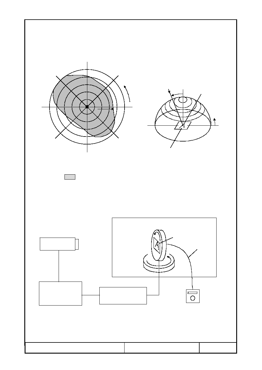
3.3. Definition of Viewing Angle and Optimum Viewing Area
*Point
�
shows the point where contrast ratio is measured. :
= 0
�
,
= -
�
*Driving condition : 1/34 Duty, 1/5 Bias, V
OD
=6.1V,
f
F
=70Hz
270
�
0
�
90
�
180
�
270
�
135
�
315
�
225
�
45
�
180
�
90
�
(
= 0
�
)
10
20
30
40
50
*Area
shows typ. CR
3 (Measuring Spot :0.3mm
)
3.4. System Block Diagram
Halogen bulb
Computer
Rotation Table (
,
)
Temperature Chamber
LCD
Optical Fiber
Waveform Generator
Control Unit &
#1980A WB
Photometer
F-51452GNFJ-AA (AA) No. 2002-0072
OPTREX CORPORATION
Page 8/16
4. I/O Terminal
4.1. Pin Assignment
CN1
No.
Symbol
Function
1
A0
H : D0~D7 are Display Data L : D0~D7 are Instructions
2
/WR
80 family CPU : Write Signal L : Active
3
/CS
Chip Select Signal L : Active
4
D7
Data Bus Line
5
D6
Data Bus Line
6
D5
Data Bus Line
7
D4
Data Bus Line
8
D3
Data Bus Line / Non-connection at 4-bit operation
9
D2
Data Bus Line / Non-connection at 4-bit operation
10
D1
Data Bus Line / Non-connection at 4-bit operation
11
D0
Data Bus Line / Non-connection at 4-bit operation
12
V
5
Power Supply for LCD Drive V
5,
V
OUT
13
V
4
Power Supply for LCD Drive V
4
= 4/5,V
5
14
V
3
Power Supply for LCD Drive V
3
= 3/5,V
5
15
V
2
Power Supply for LCD Drive V
2
= 2/5,V
5
16
V
1
Power Supply for LCD Drive V
1
= 1/5,V
5
17
VR
Voltage Adjustment Pin
Applies voltage between V
CC
and V
5
using a resistive divider.
18
V
OUT
DC/DC Voltage Converter Output
19
CAP1-
DC/DC Voltage Converter Capacitor 1 Negative Connection
20
CAP1+
DC/DC Voltage Converter Capacitor 1 Positive Connection
21
V
SS
Power Supply ( 0V, GND )
22
V
DD
Power Supply for Logic
23
/RES
Reset Signal L : Reset
F-51452GNFJ-AA (AA) No. 2002-0072
OPTREX CORPORATION
Page 9/16
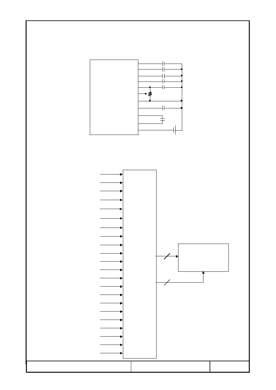
4.2. Example of Power Supply
It is recommended to apply a potentiometer for the contrast adjust due to the tolerance of the driving
voltage and its temperature dependence.
In order to suitable driving condition,please confirm reference value actual unit.
LCM
V1
V3
V2
C1:0.47
�
F
4.7
�
F
C2:0.1
�
F
4.7
�
F
VR:1
2M
V4
VR
V5
VDD
CAP1-
VOUT
CAP1+
VSS
VR
C2
C2
C2
C2
C2
C1
C1
+
+
4.3. Block Diagram
VR
VOUT
Control LSI
S1D12400
L C D P
16 Charactors
�
4Lines
SEG 80
COM 32
V3
V2
D1
V5
V4
A0
/WR
VSS
VDD
CAP1+
/RES
CAP1-
V1
/CS
D7
D6
D5
D4
D3
D2
D16B000

F-51452GNFJ-AA (AA) No. 2002-0072
OPTREX CORPORATION
Page 10/16
5. Test
No change on display and in operation under the following test condition.
Conditions: Unless otherwise specified, tests will be conducted under the following condition.
Temperature: 20
�
5
�
C
Humidity : 65
�
5%RH
tests will be not conducted under functioning state.
No.
Parameter
Conditions
Notes
1
High Temperature Operating
60
�
C
�
2
�
C, 96hrs (operation state)
2
Low Temperature Operating
-10
�
C
�
2
�
C, 96hrs (operation state)
1
3
High Temperature Storage
70
�
C
�
2
�
C, 96hrs
2
4
Low Temperature Storage
-20
�
C
�
2
�
C, 96hrs
1,2
5
Damp Proof Test
40
�
C
�
2
�
C,90~95%RH, 96hrs
1,2
6
Vibration Test
Total fixed amplitude : 1.5mm
3
Vibration Frequency : 10~55Hz
One cycle 60 seconds to 3 directions of X, Y, Z for
each 15 minutes
7
Shock Test
To be measured after dropping from 60cm high on
the concrete surface in packing state.
Note 1 :No dew condensation to be observed.
Note 2 :The function test shall be conducted after 4 hours storage at the normal
Temperature and humidity after removed from the test chamber.
Note 3 :Vibration test will be conducted to the product itself without putting it in a container.
E
A
G
D
C
F
60cm
Concrete Surface
Dropping method corner dropping
E,F,G face : once
B,C,D edge : once
A corner : once
Face dropping
Edge dropping
B
F-51452GNFJ-AA (AA) No. 2002-0072
OPTREX CORPORATION
Page 11/16
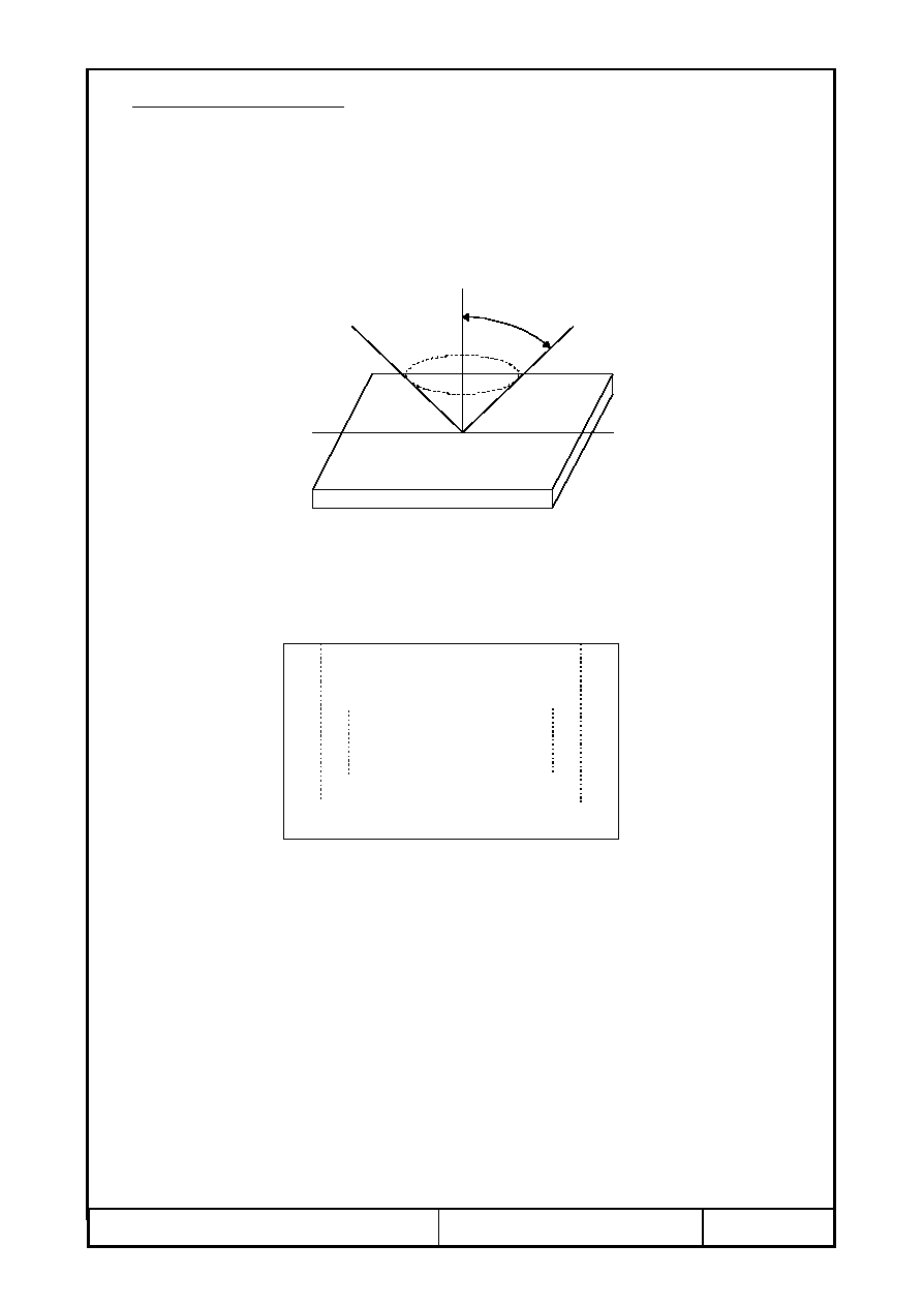
6. Appearance Standards
6.1. Inspection conditions
The LCD shall be inspected under 40W white fluorescent light.
The distance between the eyes and the sample shall be more than 30cm.
All directions for inspecting the sample should be within 45
�
against perpendicular line.
6.2. Definition of applicable Zones
A Zone : Active display area
B Zone : Out of active display area ~ Maximum seal line
C Zone : Rest parts
A Zone + B Zone = Validity viewing area
45
�
X : Maximum Seal Line
X
X
X
X
A Zone
B Zone
C Zone

F-51452GNFJ-AA (AA) No. 2002-0072
OPTREX CORPORATION
Page 12/16
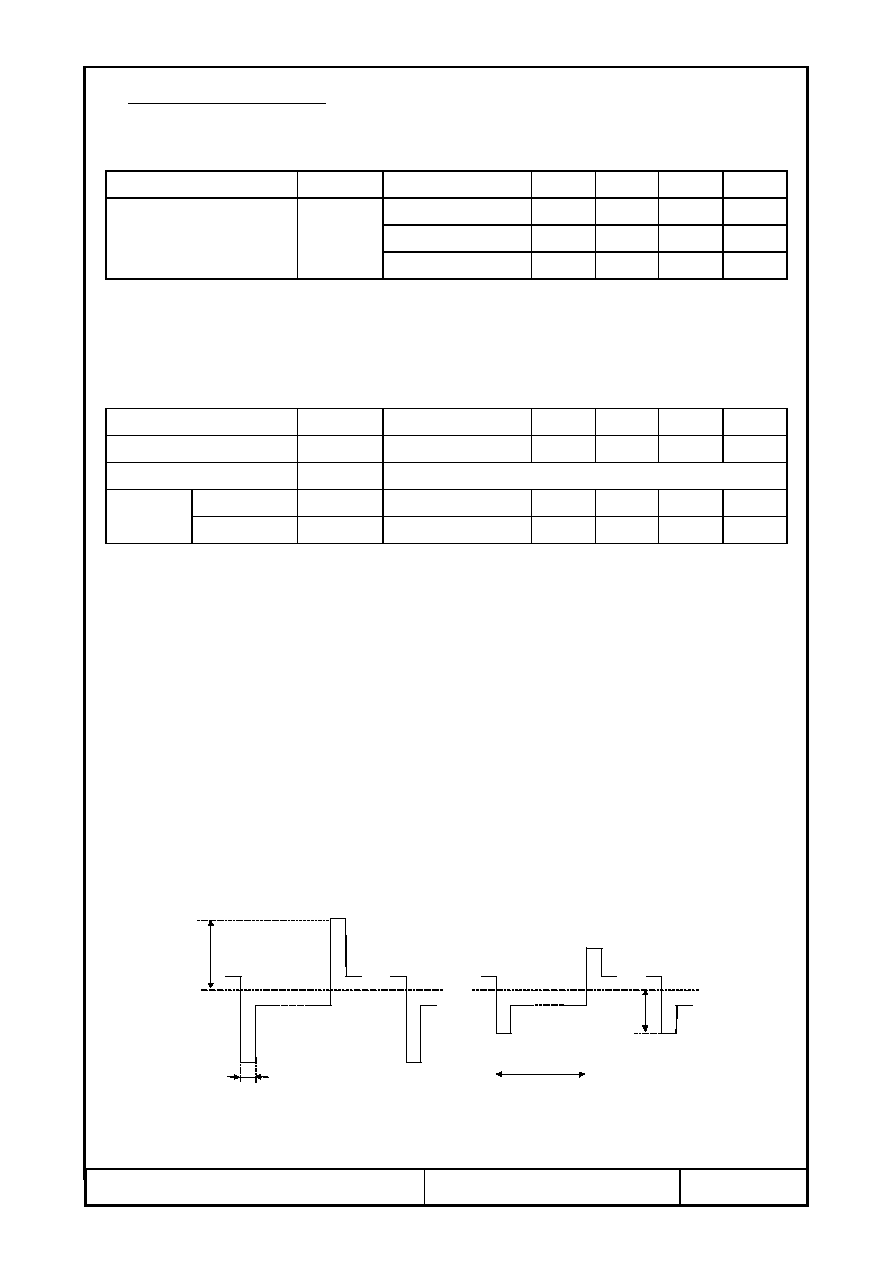
6.3. Standards
No.
Parameter
Criteria
1
Black and
(1) Round Shape
White Spots,
Zone
Acceptable Number
Foreign Substances
Dimension (mm)
A
B
C
D
0.1
*
*
*
0.1 < D
0.2
5
5
*
0.2 < D
0.3
0
1
*
0.3 < D
0
0
*
D = ( Long + Short ) / 2 * : Disregard
(2) Line Shape
Zone
Acceptable Number
X(mm) Y(mm)
A
B
C
-
0.02
W
*
*
*
2.0
L
0.03
W
3
3
*
1.0
L
0.04
W
1
2
*
1.0
L
0.05
W
0
2
*
-
0.05<W
In the same way (1)
X : Length Y : Width * : Disregard
Total defects shall not exceed 5.
2
Air Bubbles
(between glass
Zone
Acceptable Number
& polarizer)
Dimension (mm)
A
B
C
D
0.15
*
*
*
0.15< D
0.3
2
3
*
0.3 < D
0.5
1
2
*
0.5 < D
1.0
0
1
*
* : Disregard
Total defects shall not exceed 3.
F-51452GNFJ-AA (AA) No. 2002-0072
OPTREX CORPORATION
Page 13/16
No.
Parameter
Criteria
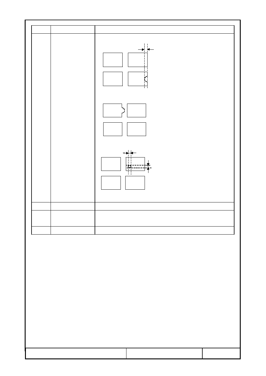
3
The Shape of Dot
(1) Dot Shape (with Dent)
As per the sketch of left hand.
(2) Dot Shape (with Projection)
Should not be connected to next dot.
(3) Pin Hole
(X+Y) / 2
0.2mm
(Less than 0.1mm is no counted.)
Total defects shall not exceed 5.
4
Polarizer Scratches
Not to be conspicuous defects.
5
Polarizer Dirts
If the stains are removed easily from LCDP surface, the module is not
not defective.
6
Color Variation
Not to be conspicuous defects.
0.15
Y
X
F-51452GNFJ-AA (AA) No. 2002-0072
OPTREX CORPORATION
Page 14/16
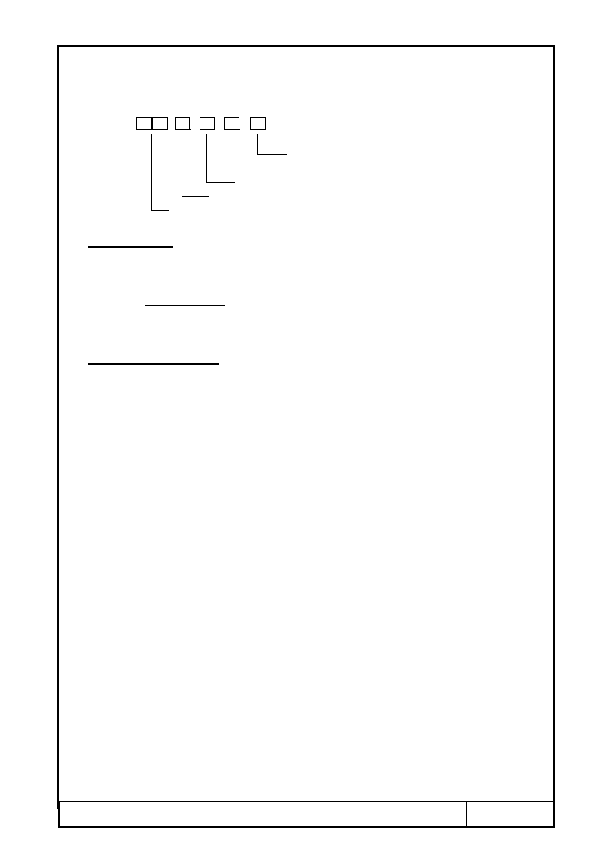
7. Code System of Production Lot
The production lot of module is specified as follows.
Factory Number (Numeral)
Factory Code (Alphabet)
Production Week (1~5)
Production Month (1~9, X, Y, Z)
Production Year (Lower 2 digits)
8. Type Number
The type number of module is specified as follows.
C-51452GNFJ-AA
9. Applying Precautions
Please contact us when questions and/or new problems not specified in this
Specifications arise.
F-51452GNFJ-AA (AA) No. 2002-0072
OPTREX CORPORATION
Page 15/16
10. Precautions Relating Product Handling
The Following precautions will guide you in handling our product correctly.
1) Liquid crystal display devices
1. The liquid crystal display device panel used in the liquid crystal display module is
made of plate glass. Avoid any strong mechanical shock. Should the glass break
handle it with care.
2. The polarizer adhering to the surface of the LCD is made of a soft material.
Guard against scratching it.
2) Care of the liquid crystal display module against static electricity discharge.
1. When working with the module, be sure to ground your body and any electrical
equipment you may be using. We strongly recommend the use of anti static mats
( made of rubber ), to protect work tables against the hazards of electrical shock.
2. Avoid the use of work clothing made of synthetic fibers. We recommend cotton
clothing or other conductivity-treated fibers.
3. Slowly and carefully remove the protective film from the LCD module, since this
operation can generate static electricity.
3) When the LCD module alone must be stored for long periods of time:
1. Protect the modules from high temperature and humidity.
2. Keep the modules out of direct sunlight or direct exposure to ultraviolet rays.
3. Protect the modules from excessive external forces.
4) Use the module with a power supply that is equipped with an overcurrent protector
circuit,since the module is not provided with this protective feature.
5) Do not ingest the LCD fluid itself should it leak out of a damaged LCD module. Should
hands or clothing come in contact with LCD fluid, wash immediately with soap.
6) Conductivity is not guaranteed for models that use metal holders where solder
connections between the metal holder and the PCB are not used. Please contact us
to discuss appropriate ways to assure conductivity.
7) For models which use CFL:
1. High voltage of 1000V or greater is applied to the CFL cable connector area.
Care should be taken not to touch connection areas to avoid burns.
2. Protect CFL cables from rubbing against the unit and thus causing the wire jacket to
become worn.
3. The use of CFLs for extended periods of time at low temperatures will significantly
shorten their service life.
8) For models which use touch panels:
1. Do not stack up modules since they can be damaged by components on neighboring
modules.
2. Do not place heavy objects on top of the product. This could cause glass breakage.
9) For models which use COG,TAB,or COF:
1. The mechanical strength of the product is low since the IC chip faces out unprotected
from the rear. Be sure to protect the rear of the IC chip from external forces.
2. Given the fact that the rear of the IC chip is left exposed, in order to protect the unit
from electrical damage, avoid installation configurations in which the rear of the IC
chip runs the risk of making any electrical contact.

F-51452GNFJ-AA (AA) No. 2002-0072
OPTREX CORPORATION
Page 16/16
10) Models which use flexible cable, heat seal, or TAB:
1. In order to maintain reliability, do not touch or hold by the connector area.
2. Avoid any bending, pulling, or other excessive force, which can result in broken
connections.
11) have an adverse effect on connecting parts ( LCD panel-TCP / HEAT SEAL / FPC /
etc., PCB-TCP / HEAT SEAL / FPC etc., TCP-HEAT SEAL, TCP-FPC, HEAT SEAL-FPC,
etc.,) depending on its materials.
Please check and evaluate these materials carefully before use.
12) In case of acrylic plate is attached to front side of LCD panel, cloudiness ( very small
cracks ) can occur on acrylic plate, being influenced by some components generated
from polarizer film..
Please check and evaluate those acrylic materials carefully before use.
11. Warranty
This product has been manufactured to your company's specifications as a part for use in
your company's general electronic products. It is guaranteed to perform according to
delivery specifications. For any other use apart from general electronic equipment, we
cannot take responsibility if the product is used in medical devices, nuclear power control
equipment, aerospace equipment, fire and security systems, or any other applications in
which there is a direct risk to human life and where extremely high levels of reliability are
required. If the product is to be used in any of the above applications, we will need to enter
into a separate product liability agreement.
1. We cannot accept responsibility for any defect, which may arise from additional
manufacturing of the product (including disassembly and reassembly), after
product delivery.
2. We cannot accept responsibility for any defect, which may arise after the application
of strong external force to the product.
3. We cannot accept responsibility for any defect, which may arise due to the application
of static electricity after the product has passed your company's acceptance inspection
procedures.
4. When the product is in CFL models, CFL service life and brightness will vary
According to the performance of the inverter used, leaks, etc. We cannot accept
responsibility for product performance, reliability, or defect, which may arise.
5. We cannot accept responsibility for intellectual property of a third party, which may
arise through the application of our product to your assembly with exception to those
issues relating directly to the structure or method of manufacturing of our product.
6. Optrex will not be held responsible for any quality guarantee issue for defect products
judged as Optrex-origin longer than 2 (two) years from Optrex production or 1(one)
year from Optrex, Optrex America, Optrex Europe, Display LC delivery which ever
comes later.