
Version 2.3, April 11, 2003
Proprietary to OmniVision Technologies
1
Advanced Information
Preliminary Datasheet
OV9620 Color CMOS SXGA (1.3 MPixel) C
AMERA
C
HIPTM
OV9121 B&W CMOS SXGA (1.3 MPixel) C
AMERA
C
HIPTM
O
mni
TM
ision
General Description
The OV9620 (color) and OV9121 (black and white) are
high-performance 1.3 mega-pixel C
AMERA
C
HIPSTM
for
digital still image and video camera products.
Both devices incorporate a 1280 x 1024 (SXGA) image
array and an on-chip 10-bit A/D converter capable of
operating at up to 15 frames per second (fps) with full
resolution. Proprietary sensor technology utilizes
advanced algorithms to cancel Fixed Pattern Noise
(FPN), eliminate smearing, and drastically reduce
blooming. The control registers allow for flexible control of
timing, polarity, and CameraChip operation, which, in turn,
allows the engineer a great deal of freedom in product
design.
Features
�
Optical Black Level Calibration (BLC)
�
Video or snapshot operations
�
Programmable/Auto Exposure and Gain Control
�
Programmable/Auto White Balance Control
�
Horizontal and vertical sub-sampling (4:2 and 4:2)
�
Programmable image windowing
�
Variable frame rate control
�
On-chip R/G/B channel and luminance average
counter
�
Internal/External frame synchronization
�
SCCB slave interface
�
Power-on reset and power-down mode
Ordering Information
Product
Package
OV9620 (Color, SXGA, VGA)
CLCC-48
OV9121 (B&W, SXGA, VGA)
CLCC-48
Applications
�
Digital still cameras
�
PC camera/dual mode
�
Video conference applications
�
Machine vision
�
Security cameras
�
Biometrics
Key Specifications
Figure 1 OV9620/OV9121 Pin Diagram
Array Size
SXGA 1280 x 1024
VGA 640 x 480
Power Supply 3.3 VDC and 2.5VDC (+5%)
Power
Requirements
Active < 50 mA
Standby < 10 �A
Output Formats (10-bit) Raw RGB Data
Lens Size 1/2"
Max. Image
Transfer Rate
SXGA 15 fps
VGA 30 fps
Sensitivity 1.0 V/Lux-sec
S/N Ratio 54 dB
Dynamic Range 60 dB (due to ADC limitations)
Scan Mode Progressive
Gamma Correction N/A
Electronics
Exposure
SXGA Up to 1050:1
VGA Up to 500:1
Pixel Size 5.2 �m x 5.2 �m
Dark Current 28 mV/s
Fixed Pattern Noise < 0.03% of V
PEAK-TO-PEAK
Image Area 6.66 mm x 5.32 mm
Package Dimensions .560 in. x .560 in.
25
D1
24
D0
23
DG
ND
22
DV
DD
21
AD
G
N
D
20
A
D
VD
D
19
Vr
A
D
2
30
XC
L
K
2
29
XC
L
K
1
28
D4
27
D3
26
D2
36
D9
37
DOVDD
38
DOGND
39
HREF
40
CHSYNC
41
VSYNC
42
NC
31
PCLK
32
D5
33
D6
34
D7
35
D8
13 VGA
12 EXPSTB
11 SCCB_E
10 RESET
9
SRAMT
8
FREX
7
PWDN
18 ASUB
17 AGND
16 AVDD
15 VcCHG
14 FSIN
48
SG
N
D
1
SV
D
D
2
Vr
H
I
G
H
3
NB
I
T
4
D
E
VD
D
5
DE
G
N
D
6
Vr
L
O
W
43
NC
44
NC
45
SI
O
_
D
46
SI
O
_
C
47
Vc
C
H
G
OV9620/OV9121

2
Proprietary to OmniVision Technologies
Version 2.3, April 11, 2003
OV9620/OV9121
CMOS SXGA (1.3 MPixel) C
AMERA
C
HIP
TM
O
mni
ision
Functional Description
Figure 2
shows the functional block diagram of the OV9620/OV9121 image sensor. The OV9620/OV9121 includes:
�
Image Sensor Array
(1280 x 1024 resolution)
�
Gain Control
�
Channel Balance
�
10-Bit Analog-to-Digital Converter
�
Black Level Compensation
�
SCCB Interface
�
Digital Video Port
�
Timing Generator
Figure 2 Functional Block Diagram
Column Sense Amps
Ro
w
S
e
l
e
c
t
Image Array
(1312 x 1036)
AMP
Gain
Control
Balance
Control
Channel
Balance
10-Bit
A/D
Timing Generator and Control Logic
PLL
RESET
PWDN
FSI
VGA
FREX
EXPSTB
XCLK
Black Level
Compensation
Digital
Video
Port
D[9:0]
PCLK
HREF
HSYNC
VSYNC
SCCB Slave
Interface
Control
Register
Bank
SIO_C
SIO_D SCCB_E

Functional Description
Version 2.3, April 11, 2003
Proprietary to OmniVision Technologies
3
O
mni
ision
Image Sensor Array
The OV9620/OV9121 sensor is a 1/2-inch format CMOS
imaging device. The sensor contains 1,359,232 pixels.
Figure 3
shows the active regions of sensor array.
Figure 3 Sensor Array Region
The color filters are Bayer pattern. The primary color
BG/GR array is arranged in line-alternating fashion. Of the
1,359,232 pixels, 1,310,720 are active. The other pixels
are used for black level calibration and interpolation.
The sensor array design is based on a field integration
read-out system with line-by-line transfer and an
electronic shutter with a synchronous pixel read-out
scheme.
Gain Control
When the column sample/hold circuit has sampled one
row of pixels, the pixel data will shift out one-by-one into
an analog amplifier. The amplifier gain can either be
programmed by the user or controlled by the internal
automatic gain control circuit (AGC). The gain adjustment
range is 0-24 dB.
Channel Balance
The amplified signals are then balanced with a channel
balance block. In this block, Red/Blue channel gain is
increased or decreased to match Green channel
luminance level and gamma correction is performed. The
adjustment range is 54 dB. This function can be done
manually by the user or with the internal automatic white
balance controller (AWB).
R
G
R
G
R
G
R
G
R
G
R
G
G
B
G
B
G
B
G
B
G
B
G
B
R
G
R
G
R
G
R
G
R
G
R
G
G
B
G
B
G
B
G
B
G
B
G
B
R
G
R
G
R
G
R
G
R
G
R
G
G
B
G
B
G
B
G
B
G
B
G
B
R
G
R
G
R
G
R
G
R
G
R
G
G
B
G
B
G
B
G
B
G
B
G
B
R
G
R
G
R
G
R
G
R
G
R
G
G
B
G
B
G
B
G
B
G
B
G
B
R
G
R
G
R
G
R
G
R
G
R
G
G
B
G
B
G
B
G
B
G
B
G
B
R
G
R
G
R
G
R
G
R
G
R
G
G
B
G
B
G
B
G
B
G
B
G
B
0
1
2
3
4
5
6
7
8
9
10
11
1035
1034
1033
0
1
2
3
4
5
1306
1307
1308
1309
1310
1311
Column
Dummy
Dummy
Dummy
Dummy
Dummy
Dummy
Optical
Black
Dummy
Dummy
Dummy
Dummy
1032
1024
Active
Lines
R
o
w
10-Bit Analog-to-Digital Converter
The balanced signal then will be digitized by the on-chip
10-bit ADC. It can operate at up to 12 MHz, and is fully
synchronous to the pixel clock. The actual conversion rate
is determined by the frame rate.
Black Level Compensation
After the pixel data has been digitized, black level
calibration can be performed before the data is output.
The black level calibration block subtracts the average
signal level of optical black pixels to compensate for the
dark current in the pixel output. Black level calibration can
be disabled by the user.
Windowing
OV9620/OV9121 allows the user to define window size or
region of interest (ROI), as required by the application.
Window size setting (in pixels) ranges from 2 x 4 to
1280 x 1024 (SXGA) or 2 x 2 to 640 x 480 (VGA), and can
be anywhere inside the 1312 x 1036 boundary. Note that
modifying window size or window position does not alter
the frame or pixel rate. The windowing control merely
alters the assertion of the HREF signal to be consistent
with the programmed horizontal and vertical ROI. The
default window size is 1280 x 1024. See
Figure 4
and
registers
HREFST
,
HREFEND
,
VSTRT
,
VEND
, and
COMM
for details.
Figure 4 Windowing
Column
End
Sensor Array
Boundary
HREF
HR
E
F
Column
Display
Window
Column
Start
Row Start
Row End
R
o
w

4
Proprietary to OmniVision Technologies
Version 2.3, April 11, 2003
OV9620/OV9121
CMOS SXGA (1.3 MPixel) C
AMERA
C
HIP
TM
O
mni
ision
Sub-sampling Mode
Default resolution for the OV9620/OV9121 is 1280 x 1024
pixels, with all active pixels being output (see
Figure 5
).
The OV9620/OV9121 can be programmed to output in
640 x 480 (VGA) sized images for applications where
higher resolution image capture is not required.
Figure 5 Pixel Array
For VGA resolution, the following sub-sampling method is
available:
Progressive Sub-sampling
The entire array is sub-sampled for maximal image
quality. Both horizontal and vertical pixels are
sub-sampled to an aspect ration of 4:2 as illustrated in
Figure 6
.
Figure 6 Sub-Sampling Mode
i
i+1
n
n+7
n+6
n+5
n+4
n+1
n+2
n+3
Row #
i+2 i+3 i+4 i+5 i+6 i+7 i+8 i+9
Column #
B
G
R
G
B
G
R
G
B
G
R
G
B
G
R
G
B
G
R
G
B
G
R
G
B
G
R
G
B
G
R
G
B
G
R
G
B
G
R
G
B
G
R
G
B
G
R
G
B
G
R
G
B
G
R
G
B
G
R
G
B
G
R
G
B
G
R
G
B
G
R
G
B
G
R
G
B
G
R
G
n
n+1
n+2
n+3
n+4
n+5
n+6
n+7
i
i+1
i+
2
i+3
i+4
i+
5
i+
6
i+7
i+8
i+9
Column
Row
Skipped Pixels
B
B
B
B
B
B
G
G
G
G
G
G
R
R
R
R
R
R
G
G
G
G
G
G
Slave Operation Mode
The OV9620/OV9121 can be programmed to operate in
slave mode (default is master mode).
When used as a slave device, the OV9620/OV9121
changes the HSYNC and VSYNC outputs to input pins for
use as horizontal and vertical synchronization input
triggers supplied by the master device. The master device
must provide the following signals:
1.
System clock MCLK to XCLK1 pin
2.
Horizontal sync MHSYNC to CHSYNC pin
3.
Vertical frame sync MVSYNC to VSYNC pin
See
Figure 7
for slave mode connections and
Figure 8
for
detailed timing considerations. In this mode, the clock for
all devices should be the same. Otherwise, the devices
will suffer from flickering at line frequency.
Figure 7 Slave Mode Connection
Figure 8 Slave Mode Timing
Channel Average Calculator
OV9620/OV9121 provides average output level data for
the R/G/B channels along with frame-averaged luminance
level. Access to the data is via the serial control port.
Average values are calculated from 128 pixels per line (64
in VGA).
D[9:0]
CHSYNC
VSYNC
XCLK1
MHSYNC
MVSYNC
MCLK
Master
Device
OV9620
(OV9120)
NOTE:
1) T
HS
> 6 T
clk
, Tvs > T
line
2) T
line
= 1520 x T
clk
(SXGA); T
line
= 800 x T
clk
(VGA)
3) T
frame
= 1050 x T
line
(SXGA); T
frame
= 500 x T
line
(VGA)
T
frame
T
VS
T
line
T
clk
T
HS
VSYNC
HSYNC
MCLK
Functional Description
Version 2.3, April 11, 2003
Proprietary to OmniVision Technologies
5
O
mni
ision
Reset
OV9620/OV9121 includes a RESET pin (pin 10 - see
"RESET" on page 7
) that forces a complete hardware
reset when it is pulled high (VCC). OV9620/OV9121
clears all registers and resets them to their default values
when a hardware reset occurs. Reset can also be initiated
through the SCCB interface.
Power-Down Mode
There are two ways to place OV9620/OV9121 into
power-down mode: hardware power-down and SCCB
software power-down.
To initiate hardware power-down, the PWDN pin (pin 7 -
see
"PWDN" on page 7
) must be tied to high (+3.3 VDC).
When this occurs, the OV9620/OV9121 internal device
clock is halted and all internal counters are reset. The
current draw is less than 10 �A in this standby mode.
Executing a software power-down through the SCCB
interface suspends internal circuit activity, but does not
halt the device clock. The current requirements drop to
less than 1mA in this mode. All register content is
maintained in standby mode
SCCB Interface
OV9620/OV9121 provides an on-chip SCCB serial control
port that allows access to all internal registers, for
complete control and monitoring of OV9620/OV9121
operation.
Refer to
OmniVision Technologies Serial Camera Control
Bus (SCCB) Specification
for detailed usage of the SCCB
interface.
Video Output
RGB Raw Data Output
The OV9620 C
AMERA
C
HIP
offers 10-bit RGB raw data
output.
B&W Output
The OV9121 offers 10-bit luminance signal data output.
Digital Video Port
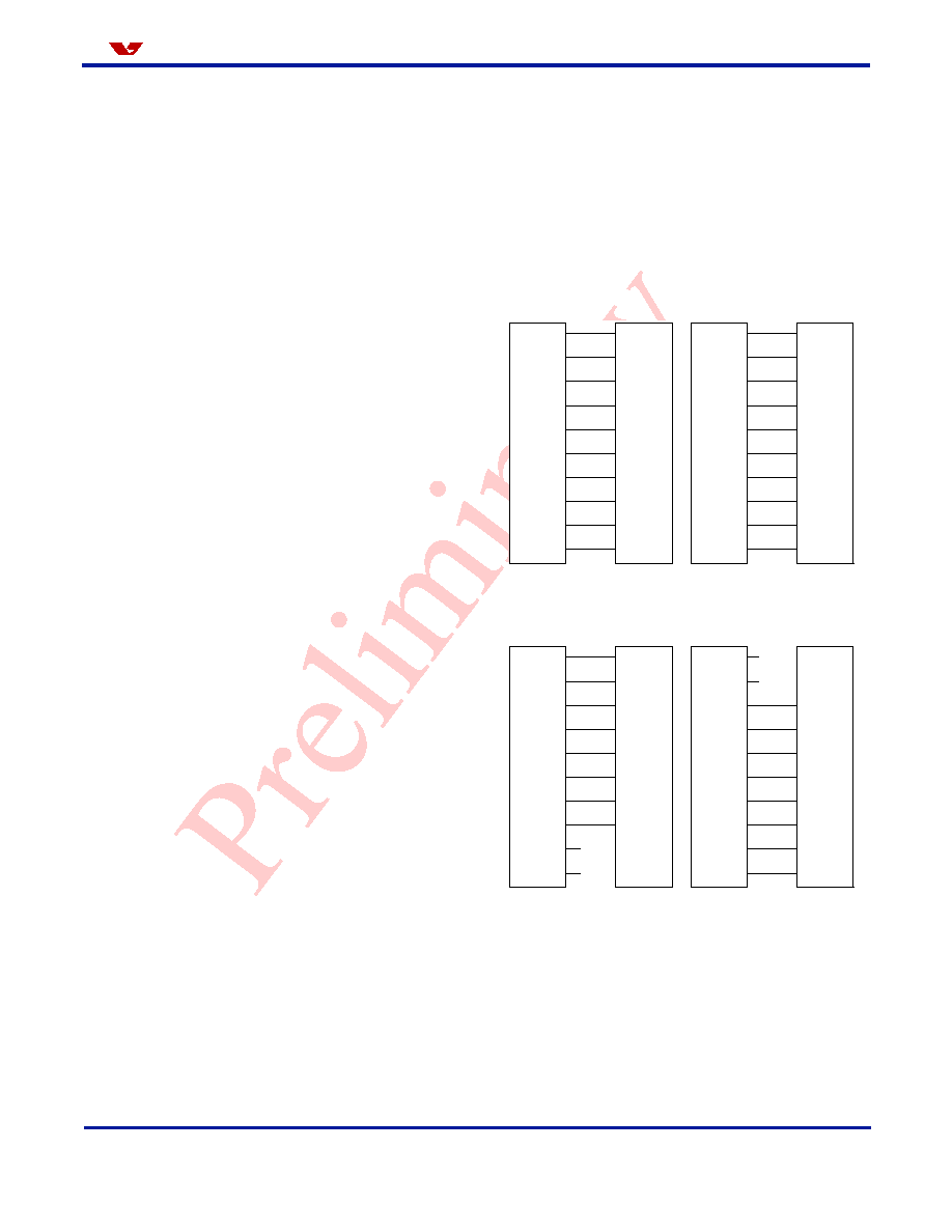
MSB/LSB Swap
OV9620/OV9121 has a 10-bit digital video port. The MSB
and LSB can be swapped with the control registers.
Figure 9
shows some examples of connections with
external devices.
Figure 9 Connection Examples
D7
D6
D5
D4
D3
D2
D1
LSB D0
D7
D6
D5
D4
D3
D2
D1
D0
D7
D6
D5
D4
D3
D2
D1
MSB D0
D2
D3
D4
D5
D6
D7
D8
D9
External
Device
OV9620
(OV9120)
External
Device
OV9620
(OV9120)
MSB D9
D8
D9
D8
LSB D9
D8
D0
D1
Default 10-bit Connection
Swap 10-bit Connection
D7
D6
D5
D4
D3
D2
D1
LSB D0
D5
D4
D3
D2
D1
D0
D7
D6
D5
D4
D3
D2
D1
MSB D0
D0
D1
D2
D3
D4
D5
D6
D7
External
Device
OV9620
(OV9120)
External
Device
OV9620
(OV9120)
MSB D9
D8
D7
D6
LSB D9
D8
Default 8-bit Connection
Swap 8-bit Connection