
1
Transistor
2SC1473, 2SC1473A
Silicon NPN triple diffusion planer type
For general amplification
2SC1473 complementary to 2SA1018
2SC1473A complementary to 2SA1767
s
Features
q
High collector to emitter voltage V
CEO
.
q
High transition frequency f
T
.
s
Absolute Maximum Ratings
(Ta=25įC)
Unit: mm
Parameter
Collector to
base voltage
Collector to
emitter voltage
Emitter to base voltage
Peak collector current
Collector current
Collector power dissipation
Junction temperature
Storage temperature
1:Emitter
2:Collector
3:Base
JEDEC:TO≠92
EIAJ:SC≠43A
5.0
Ī
0.2
4.0
Ī
0.2
5.1
Ī
0.2
13.5
Ī
0.5
0.45
+0.2
≠0.1
0.45
+0.2
≠0.1
1.27
1.27
2.3
Ī
0.2
2.54
Ī
0.15
2
1
3
Symbol
V
CBO
V
CEO
V
EBO
I
CP
I
C
P
C
T
j
T
stg
Ratings
250
300
200
300
7
100
70
750
150
≠55 ~ +150
Unit
V
V
V
mA
mA
mW
įC
įC
2SC1473
2SC1473A
2SC1473
2SC1473A
s
Electrical Characteristics
(Ta=25įC)
Parameter
Collector cutoff
current
Collector to emitter
voltage
Emitter to base voltage
Forward current transfer ratio
Collector to emitter saturation voltage
Transition frequency
Collector output capacitance
Symbol
I
CEO
V
CEO
V
EBO
h
FE
*
V
CE(sat)
f
T
C
ob
Conditions
V
CE
= 120V, I
B
= 0
V
CE
= 120V, I
B
= 0
I
C
= 100
Ķ
A, I
C
= 0
I
E
= 1
Ķ
A, I
C
= 0
V
CE
= 10V, I
C
= 5mA
I
C
= 50mA, I
B
= 5mA
V
CB
= 10V, I
E
= ≠10mA, f = 200MHz
V
CB
= 10V, I
E
= 0, f = 1MHz
min
200
300
7
30
50
typ
80
max
1
1
220
1.2
10
Unit
Ķ
A
V
V
V
MHz
pF
*
h
FE
Rank classification
Rank
P
Q
R
h
FE
30 ~ 100
60 ~ 150
100 ~ 220
2SC1473
2SC1473A
2SC1473
2SC1473A
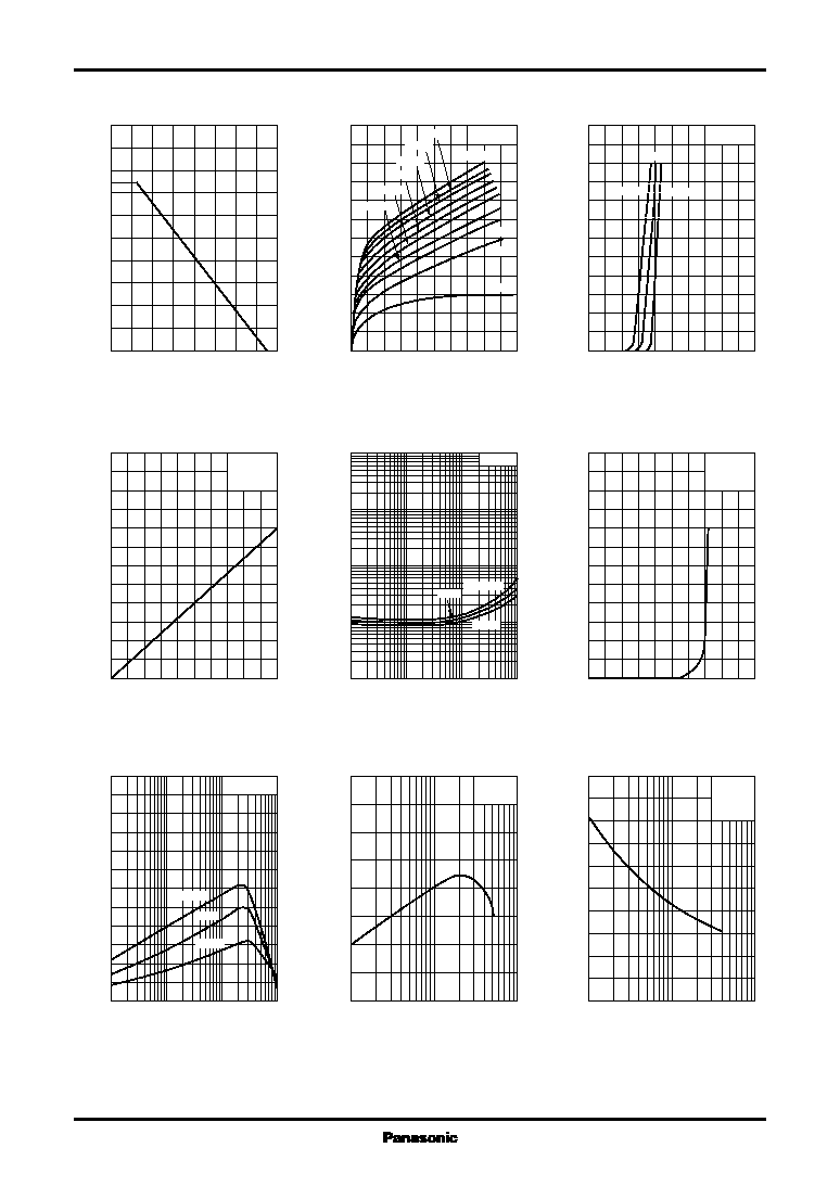
2
Transistor
2SC1473, 2SC1473A
P
C
-- Ta
I
C
-- V
CE
I
C
-- V
BE
I
C
-- I
B
V
CE(sat)
-- I
C
I
B
-- V
BE
h
FE
-- I
C
f
T
-- I
E
C
ob
-- V
CB
0
160
40
120
80
140
20
100
60
0
1.0
0.8
0.6
0.4
0.2
0.9
0.7
0.5
0.3
0.1
Ambient temperature Ta (įC)
Collector power dissipation P
C
(W
)
0
10
8
2
6
4
0
120
100
80
60
40
20
I
B
=2mA
1.8mA
1.6mA
1.4mA
1.2mA
1.0mA
0.8mA
0.2mA
0.4mA
0.6mA
Ta=25įC
Collector to emitter voltage V
CE
(V)
Collector current I
C
(mA
)
0
2.0
1.6
0.4
1.2
0.8
0
120
100
80
60
40
20
V
CE
=10V
Ta=75įC
≠25įC
25įC
Base to emitter voltage V
BE
(V)
Collector current I
C
(mA
)
0
2.0
1.6
0.4
1.2
0.8
0
120
100
80
60
40
20
V
CE
=10V
Ta=25įC
Base current I
B
(mA)
Collector current I
C
(mA
)
0.1
1
10
100
0.3
3
30
0.01
0.03
0.1
0.3
1
3
10
30
100
I
C
/I
B
=10
Ta=75įC
25įC
≠25įC
Collector current I
C
(mA)
Collector to emitter saturation voltage V
CE(sat)
(V
)
0
1.0
0.8
0.2
0.6
0.4
0
3.0
2.5
2.0
1.5
1.0
0.5
V
CE
=10V
Ta=25įC
Base to emitter voltage V
BE
(V)
Base current I
B
(mA
)
0.1
1
10
100
0.3
3
30
0
360
300
240
180
120
60
V
CE
=10V
Ta=75įC
25įC
≠25įC
Collector current I
C
(mA)
Forward current transfer ratio h
FE
≠1
≠3
≠10
≠30
≠100
0
160
120
40
100
140
80
20
60
V
CB
=10V
Ta=25įC
Emitter current I
E
(mA)
Transition frequency f
T
(MHz
)
1
3
10
30
100
0
10
8
6
4
2
9
7
5
3
1
I
E
=0
f=1MHz
Ta=25įC
Collector to base voltage V
CB
(V)
Collector output capacitance C
ob
(pF
)
3
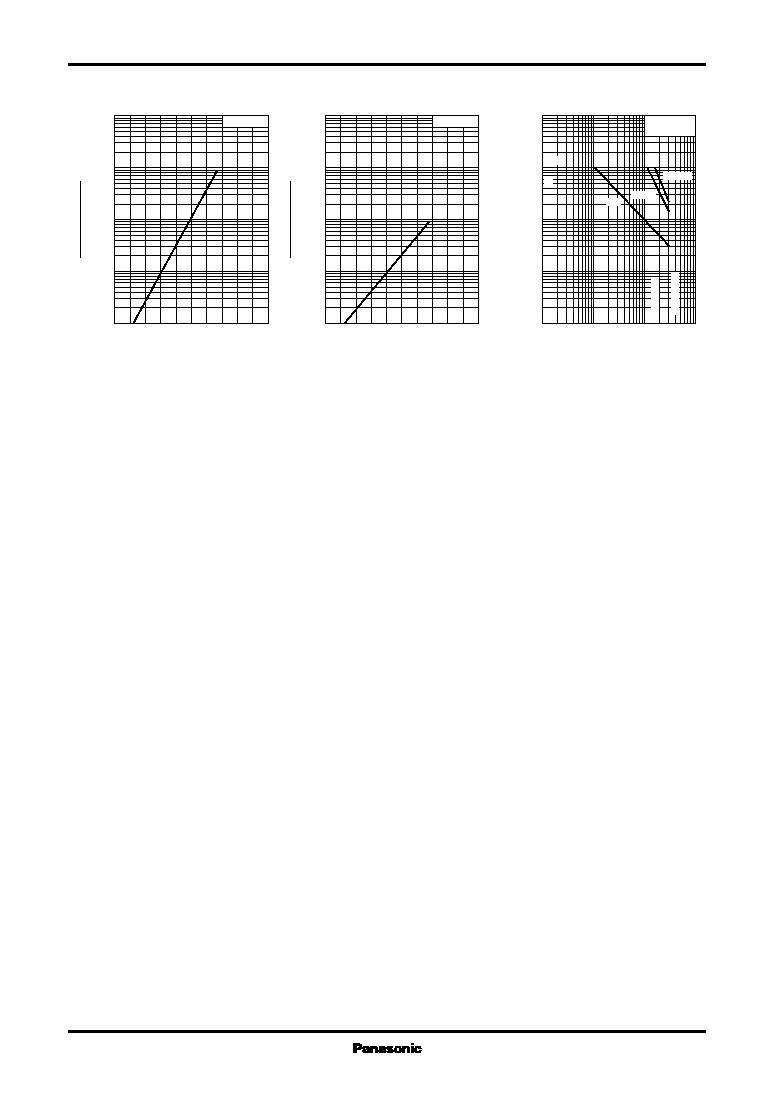
Transistor
2SC1473, 2SC1473A
I
CBO
-- Ta
I
EBO
-- Ta
Area of safe operation (ASO)
0
200
160
40
120
80
1
10
10
2
10
3
10
4
V
CB
=250V
Ambient temperature Ta (įC)
I
CBO
(Ta
)
I
CBO
(Ta=25įC
)
0
200
160
40
120
80
1
10
10
2
10
3
10
4
V
EB
=5V
Ambient temperature Ta (įC)
I
EBO
(Ta
)
I
EBO
(Ta=25įC
)
1
10
100
1000
3
30
300
0.1
0.3
1
3
10
30
100
300
1000
Single pulse
Ta=25įC
t=10ms
2SC1473A
2SC1473
t=1ms
DC
I
CP
I
C
Collector to emitter voltage V
CE
(V)
Collector current I
C
(mA
)