Transistors
1
2SB0710, 2SB0710A
Silicon PNP epitaxial planer type
For general amplification
Complementary to 2SD0602 and 2SD0602A
I Features
∑ Large collector current I
C
∑ Mini type package, allowing downsizing of the equipment and
automatic insertion through the tape packing and the magazine
packing.
I Absolute Maximum Ratings T
a
= 25∞C
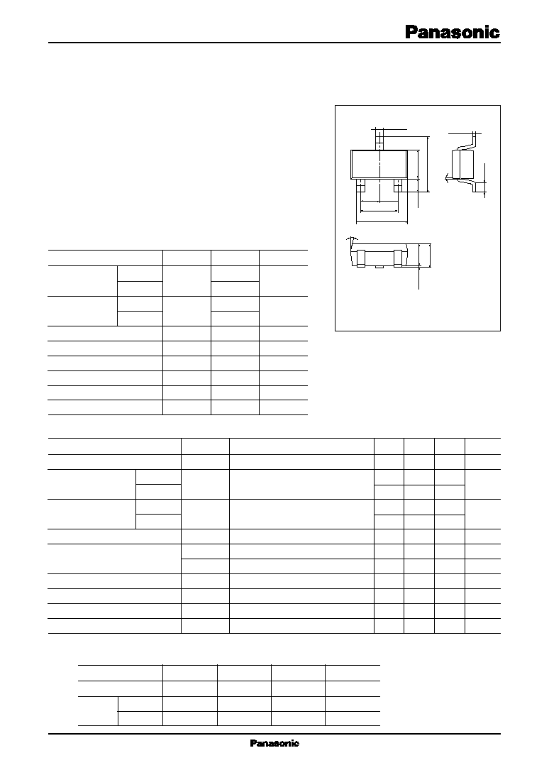
1: Base
JEDEC: TO-236
2: Emitter
EIAJ: SC-59
3: Collector
Mini Type Package
Unit: mm
Parameter
Symbol
Rating
Unit
Collector to
2SB0710
V
CBO
-30
V
base voltage
2SB0710A
-60
Collector to
2SB0710
V
CEO
-25
V
emitter voltage
2SB0710A
-50
Emitter to base voltage
V
EBO
-5
V
Peak collector current
I
CP
-1
A
Collector current
I
C
-500
mA
Collector power dissipation
P
C
200
mW
Junction temperature
T
j
150
∞C
Storage temperature
T
stg
-55 to +150
∞C
I Electrical Characteristics T
a
= 25∞C ± 3∞C
Marking Symbol
∑ 2SB0710 : C
∑ 2SB0710A : D
0.40
+0.10
≠0.05
(0.65)
1.50
+0.25 ≠0.05
2.8
+0.2 ≠0.3
2
1
3
(0.95) (0.95)
1.9
±0.1
2.90
+0.20
≠0.05
0.16
+0.10
≠0.06
0.4
±0.2
5
∞
10
∞
0 to 0.1
1.1
+0.2 ≠0.1
1.1
+0.3 ≠0.1
Parameter
Symbol
Conditions
Min
Typ
Max
Unit
Collector cutoff current
I
CBO
V
CB
= -20 V, I
E
= 0
- 0.1
µA
Collector to
2SB0710
V
CBO
I
C
= -10 µA, I
E
= 0
-30
V
base voltage
2SB0710A
-60
Collector to
2SB0710
V
CEO
I
C
= -10 mA, I
B
= 0
-25
V
emitter voltage
2SB0710A
-50
Emitter to base voltage
V
EBO
I
E
= -10 µA, I
C
= 0
-5
V
Forward current transfer ratio
*1
h
FE1
*2
V
CE
= -10 V, I
C
= -150 mA
85
340
h
FE2
V
CE
= -10 V, I
C
= -500 mA
40
Collector to emitter saturation voltage
*1
V
CE(sat)
I
C
= -300 mA, I
B
= -30 mA
- 0.35 - 0.6
V
Base to emitter saturation voltage
*1
V
BE(sat)
I
C
= -300 mA, I
B
= -30 mA
-1.1
-1.5
V
Transition frequency
f
T
V
CB
= -10 V, I
E
= 50 mA, f = 200 MHz
200
MHz
Collector output capacitance
C
ob
V
CB
= -10 V, I
E
= 0, f = 1 MHz
6
15
pF
Rank
Q
R
S
No-rank
h
FE1
85 to 170
120 to 240
170 to 340
85 to 340
Marking
2SB0710
CQ
CR
CS
C
symbol
2SB0710A
DQ
DR
DS
D
Note) *1: Pulse measurement
*2: Rank classification
Product of no-rank is not classi-
fied and have no indication for
rank.

2SB0710, 2SB0710A
Transistors
2
P
C
T
a
I
C
V
CE
I
C
I
B
V
CE(sat)
I
C
V
BE(sat)
I
C
h
FE
I
C
f
T
I
E
C
ob
V
CB
V
CER
R
BE
0
160
40
120
80
0
240
200
160
120
80
40
Ambient temperature T
a
(
∞C)
Collector power dissipation P
C
(mW
)
0
0
≠12
≠2
≠10
≠4
≠8
≠6
-1 200
-1 000
-800
-600
-400
-200
-9 mA
-8 mA
-7 mA
-6 mA
-5 mA
-4 mA
-3 mA
-2 mA
-1 mA
I
B
=
-10 mA
Collector to emitter voltage V
CE
(V)
Collector current I
C
(mA
)
T
a
= 25∞C
0
-10
-8
-6
-4
-2
0
-800
-700
-600
-500
-400
-300
-200
-100
Base current I
B
(mA)
Collector current
I
C
(mA
)
V
CE
= -10 V
T
a
= 25∞C
- 0.001
- 0.003
-1
-3
- 0.01
- 0.03
- 0.1
- 0.3
-1
-3
-10
-10 -30 -100 -300 -1 000
Collector to emitter saturation voltage
V
CE(sat)
(V
)
Collector current I
C
(mA)
I
C
/ I
B
= 10
25
∞C
-25∞C
T
a
=75∞C
-1
-3
- 0.1
- 0.3
-1
3
-10
-30
-100
-10 -30 -100 -300 -1 000
T
a
= -25∞C
25
∞C
75
∞C
Base to emitter saturation voltage
V
BE(sat)
(V
)
Collector current I
C
(mA)
I
C
/ I
B
= 10
- 0.01
- 0.03
0
600
500
400
300
200
100
-1
-3
-10
Forward current transfer ratio h
FE
V
CE
= -10 V
- 0.01 - 0.03 - 0.1 - 0.3
Collector current I
C
(A)
T
a
= 75∞C
25
∞C
-25∞C
0
240
200
160
120
80
40
1
3
10
30
100
2
20
5
50
Transition frequency f
T
(MHz
)
Emitter current I
E
(mA)
V
CB
= -10 V
T
a
= 25∞C
0
-1
24
20
16
12
8
4
-3
-10
-30
-100
-50
-20
-5
-2
Collector output capacitance C
ob
(
pF
)
Collector to base voltage V
CB
(V)
I
E
= 0
f
= 1 MHz
T
a
= 25∞C
1
3
10
30
100
300
1 000
0
-120
-100
-80
-60
-40
-20
Collector to emitter voltage V
CER
(V
)
Base to emitter resistance R
BE
(k
)
I
C
= -2 mA
T
a
= 25∞C
2SB0710A
2SB0710