1
Transistor
2.1
±
0.1
1.3
±
0.1
0.9
±
0.1
0.7
±
0.1
0.3
+0.1
≠0
0.15
+0.1
≠0.05
2.0
±
0.2
1.25
±
0.1
0.425
0.425
1
3
2
0.65
0.2
0.65
0 to 0.1
0.2
±
0.1
2SB1218A
Silicon PNP epitaxial planer type
For general amplification
Complementary to 2SD1819A
s
Features
q
High foward current transfer ratio h
FE
.
q
S-Mini type package, allowing downsizing of the equipment and
automatic insertion through the tape packing and the magazine
packing.
s
Absolute Maximum Ratings
(Ta=25∞C)
Unit: mm
Parameter
Collector to base voltage
Collector to emitter voltage
Emitter to base voltage
Peak collector current
Collector current
Collector power dissipation
Junction temperature
Storage temperature
1:Base
2:Emitter
EIAJ:SC≠70
3:Collector
S-Mini Type Package
Symbol
V
CBO
V
CEO
V
EBO
I
CP
I
C
P
C
T
j
T
stg
Ratings
≠45
≠45
≠7
≠200
≠100
150
150
≠55 ~ +150
Unit
V
V
V
mA
mA
mW
∞C
∞C
s
Electrical Characteristics
(Ta=25∞C)
Parameter
Collector cutoff current
Collector to base voltage
Collector to emitter voltage
Emitter to base voltage
Forward current transfer ratio
Collector to emitter saturation voltage
Transition frequency
Collector output capacitance
Symbol
I
CBO
I
CEO
V
CBO
V
CEO
V
EBO
h
FE
*
V
CE(sat)
f
T
C
ob
Conditions
V
CB
= ≠20V, I
E
= 0
V
CE
= ≠10V, I
B
= 0
I
C
= ≠10
µ
A, I
E
= 0
I
C
= ≠2mA, I
B
= 0
I
E
= ≠10
µ
A, I
C
= 0
V
CE
= ≠10V, I
C
= ≠2mA
I
C
= ≠100mA, I
B
= ≠10mA
V
CB
= ≠10V, I
E
= 1mA, f = 200MHz
V
CB
= ≠10V, I
E
= 0, f = 1MHz
min
≠45
≠45
≠7
160
typ
≠ 0.3
80
2.7
max
≠0.1
≠100
460
≠ 0.5
Unit
µ
A
µ
A
V
V
V
V
MHz
pF
*
h
FE
Rank classification
Rank
Q
R
S
h
FE
160 ~ 260
210 ~ 340
290 ~ 460
Marking Symbol
BQ
BR
BS
Marking symbol :
B
2
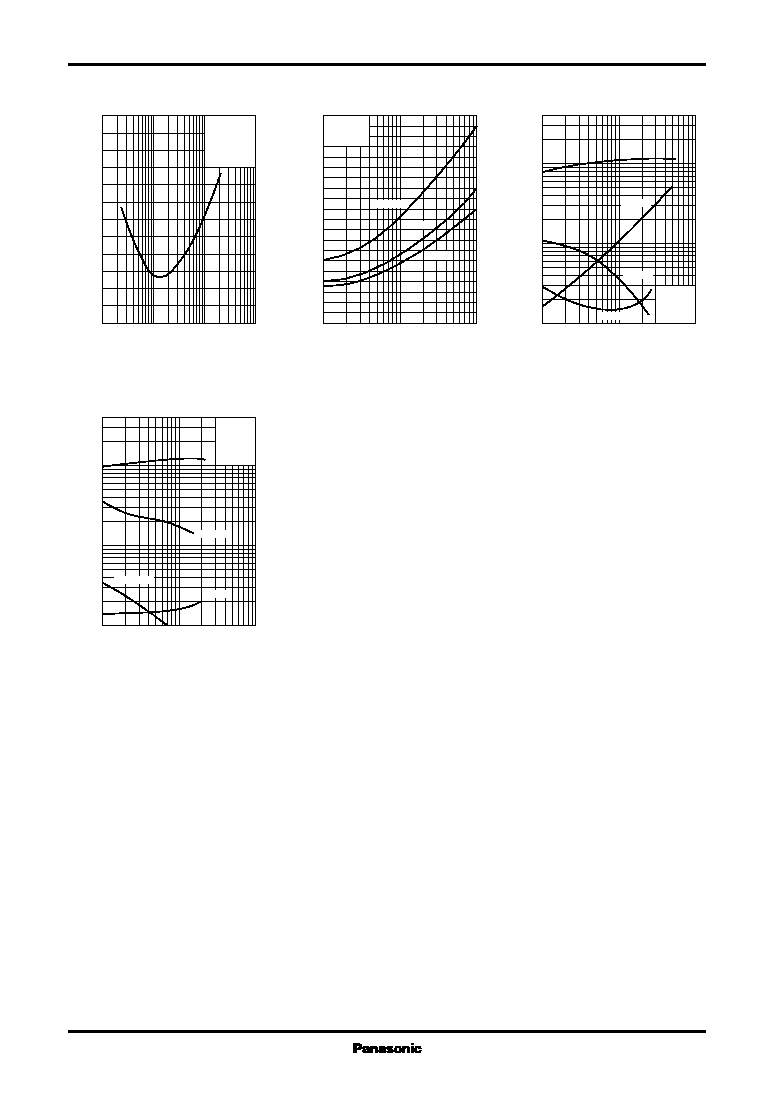
Transistor
2SB1218A
0
160
40
120
80
140
20
100
60
0
240
200
160
120
80
40
Ambient temperature Ta (∞C)
Collector power dissipation P
C
(mW
)
0
≠12
≠10
≠8
≠2
≠6
≠4
0
≠120
≠100
≠80
≠60
≠40
≠20
Ta=25∞C
≠250
µ
A
≠200
µ
A
≠150
µ
A
≠100
µ
A
≠50
µ
A
I
B
=≠300
µ
A
Collector to emitter voltage V
CE
(V)
Collector current I
C
(mA
)
0
≠450
≠150
≠300
0
≠60
≠50
≠40
≠30
≠20
≠10
V
CE
=≠5V
Ta=25∞C
Base current I
B
(
µ
A)
Collector current I
C
(mA
)
0
≠1.8
≠ 0.6
≠1.2
0
≠400
≠300
≠100
≠250
≠350
≠200
≠50
≠150
V
CE
=≠5V
Ta=25∞C
Base to emitter voltage V
BE
(V)
Base current I
B
(
µ
A
)
0
≠2.0
≠1.6
≠ 0.4
≠1.2
≠ 0.8
0
≠240
≠200
≠160
≠120
≠80
≠40
V
CE
=≠5V
Ta=75∞C
≠25∞C
25∞C
Base to emitter voltage V
BE
(V)
Collector current I
C
(mA
)
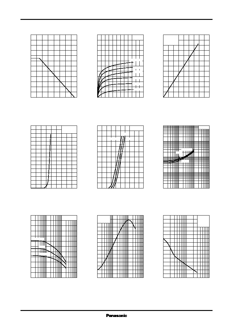
≠1
≠10
≠100
≠1000
≠3
≠30
≠300
≠ 0.001
≠ 0.003
≠ 0.01
≠ 0.03
≠ 0.1
≠ 0.3
≠1
≠3
≠10
I
C
/I
B
=10
25∞C
≠25∞C
Ta=75∞C
Collector current I
C
(mA)
Collector to emitter saturation voltage V
CE(sat)
(V
)
≠1
≠10
≠100
≠1000
≠3
≠30
≠300
0
600
500
400
300
200
100
V
CE
=≠10V
Ta=75∞C
25∞C
≠25∞C
Collector current I
C
(mA)
Forward current transfer ratio h
FE
0.1
1
10
100
0.3
3
30
0
160
120
40
100
140
80
20
60
V
CB
=≠10V
Ta=25∞C
Emitter current I
E
(mA)
Transition frequency f
T
(MHz
)
≠1
≠3
≠10
≠30
≠100
0
8
6
2
5
7
4
1
3
I
E
=0
f=1MHz
Ta=25∞C
Collector to base voltage V
CB
(V)
Collector output capacitance C
ob
(pF
)
P
C
-- Ta
I
C
-- V
CE
I
C
-- I
B
I
B
-- V
BE
I
C
-- V
BE
V
CE(sat)
-- I
C
h
FE
-- I
C
f
T
-- I
E
C
ob
-- V
CB