Transistors
1
2SC2480
Silicon NPN epitaxial planer type
For high-frequency amplification / oscillation / mixing
I Features
∑ High transition frequency f
T
∑ Mini type package, allowing downsizing of the equipment and
automatic insertion through the tape packing and the magazine
packing.
I Absolute Maximum Ratings T
a
= 25∞C
Parameter
Symbol
Rating
Unit
Collector to base voltage
V
CBO
30
V
Collector to emitter voltage
V
CEO
20
V
Emitter to base voltage
V
EBO
3
V
Collector current
I
C
50
mA
Collector power dissipation
P
C
150
mW
Junction temperature
T
j
150
∞C
Storage temperature
T
stg
-55 to +150
∞C
Parameter
Symbol
Conditions
Min
Typ
Max
Unit
Collector to base voltage
V
CBO
I
C
= 100 µA, I
E
= 0
30
V
Emitter to base voltage
V
EBO
I
E
= 10 µA, I
C
= 0
3
V
Forward current transfer ratio
h
FE
V
CB
= 10 V, I
E
= -2 mA
25
250
Base to emitter voltage
V
BE
V
CB
= 10 V, I
E
= -2 mA
720
mV
Transition frequency
*
f
T
V
CB
= 10 V, I
E
= -15 mA, f = 200 MHz
800
1 300
1 600
MHz
Common emitter reverse transfer
C
re
V
CB
= 10 V, I
E
= -1 mA, f = 10.7 MHz
1
1.5
pF
capacitance
C
rb
V
CE
= 6 V, I
C
= 0, f = 1 MHz
0.8
pF
Power gain
PG
V
CB
= 10 V, I
E
= -1 mA, f = 200 MHz
20
dB
I Electrical Characteristics T
a
= 25∞C ± 3∞C
Marking Symbol: R
Note) *: Rank classification
Rank
T
S
No-rank
f
T
(MHz)
800 to 1 400 1 000 to 1 600 800 to 1 600
Marking symbol
RT
RS
R
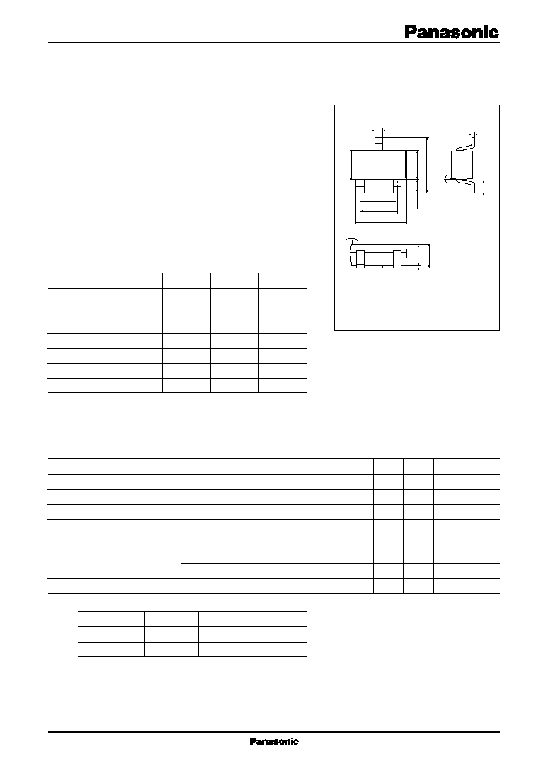
Unit: mm
0.40
+0.10
≠0.05
(0.65)
1.50
+0.25 ≠0.05
2.8
+0.2 ≠0.3
2
1
3
(0.95) (0.95)
1.9
±0.1
2.90
+0.20
≠0.05
0.16
+0.10
≠0.06
0.4
±0.2
5
∞
10
∞
0 to 0.1
1.1
+0.2 ≠0.1
1.1
+0.3 ≠0.1
1: Base
JEDEC: TO-236
2: Emitter
EIAJ: SC-59
3: Collector
Mini Type Package
Product of no-rank is not classified and have no indication for rank.

2SC2480
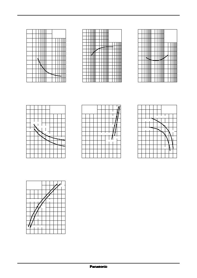
Transistors
2
P
C
T
a
I
C
V
CE
I
C
I
B
I
B
V
BE
I
C
V
BE
h
FE
I
C
V
CE(sat)
I
C
0
160
40
120
80
0
240
200
160
120
80
40
Ambient temperature T
a
(
∞C)
Collector power dissipation P
C
(mW)
0
24
20
16
12
8
4
0
4
8
12
16
2
6
10
14
18
I
B
= 300 µA
50
µA
100
µA
150
µA
200
µA
250
µA
Collector to emitter voltage V
CE
(V)
Collector current I
C
(mA)
T
a
= 25∞C
0
0
500
400
300
200
100
24
20
16
12
8
4
Base current I
B
(
µA)
Collector current
I
C
(mA)
V
CE
= 10 V
T
a
= 25∞C
0
400
350
300
250
200
150
100
50
0
2.0
1.6
1.2
0.8
0.4
V
CE
= 10 V
T
a
= 25∞C
Base to emitter voltage V
BE
(V)
Base current I
B
(
µ
A)
0
0
2.0
1.6
1.2
0.8
0.4
60
50
40
30
20
10
V
CE
= 10 V
T
a
= 75∞C
-25∞C
25
∞C
Base to emitter voltage V
BE
(V)
Collector current I
C
(mA)
0
0.1
0.3
240
200
160
120
80
40
1
3
10
30
100
T
a
= 75∞C
25
∞C
-25∞C
Forward current transfer ratio h
FE
V
CE
= 10 V
Collector current I
C
(mA)
0.01
0.03
0.1
0.3
0.1
0.3
1
3
10
30
100
1
3
10
30
100
Collector to emitter saturation voltage
V
CE(sat)
(V)
Collector current I
C
(mA)
I
C
/ I
B
= 10
T
a
= 75∞C
25
∞C
≠25
∞C
- 0.1 - 0.3
-1
-3
-10 -30 -100
0
1 600
1 400
1 200
1 000
800
600
400
200
Transition frequency f
T
(MHz)
Emitter current I
E
(mA)
V
CB
= 10 V
T
a
= 25∞C
0
2.4
2.0
1.6
1.2
0.8
0.4
0.1
0.3
1
3
10
30
100
Common emitter reverse transfer capacitance C
re
(pF)
Collector to emitter voltage V
CE
(V)
I
C
= 1 mA
f
= 10.7 MHz
T
a
= 25∞C
f
T
I
E
C
re
V
CE
Transistors
2SC2480
3
Z
rb
I
E
PG
I
E
NF
I
E
b
ib
g
ib
b
rb
g
rb
b
fb
g
fb
b
ob
g
ob
- 0.1
- 0.3
-1
- 0.5
-5
- 0.2
-2 -3
-10
Reverse transfer impedance Z
rb
(
)
0
120
100
80
60
40
20
V
CB
= 10 V
f
= 2 MHz
T
a
= 25∞C
Emitter current I
E
(mA)
- 0.1 - 0.3
-1
-3
-10 -30 -100
Power gain PG (dB)
0
40
35
30
25
20
15
10
5
V
CB
= 10 V
f
= 100 MHz
R
g
= 50
T
a
= 25∞C
Emitter current I
E
(mA)
Noise figure NF (dB)
0
12
10
8
6
4
2
- 0.1 - 0.3
-1
-3
-10 -30 -100
V
CB
= 10 V
f
= 100 MHz
R
g
= 50
T
a
= 25∞C
Emitter current I
E
(mA)
-60
0
50
40
30
20
10
0
-10
-20
-30
-40
-50
Input conductance g
ib
(mS)
Input susceptance b
ib
(mS)
y
ib
= g
ib
+ jb
ib
V
CB
= 10 V
f
= 900 MHz
I
E
= -2 mA
-5 mA
300
500
600
200
-2.4
-1.0
0
- 0.2
- 0.4
- 0.6
- 0.8
0
- 0.4
- 0.8
-1.2
-1.6
-2.0
f
= 900 MHz
I
E
= -5 mA
-2 mA
300
500
600
200
Reverse transfer conductance g
rb
(mS)
Reverse transfer susceptance b
rb
(mS)
y
rb
= g
rb
+ jb
rb
V
CB
= 10 V
0
-60
40
20
0
-20
-40
48
40
32
24
16
8
-2 mA
300
500
600
900
f
= 200 MHz
I
E
= -5 mA
Forward transfer conductance g
fb
(mS)
Forward transfer susceptance b
fb
(mS)
y
fb
= g
fb
+ jb
fb
V
CB
= 10 V
0
0
2.0
1.6
1.2
0.8
0.4
12
10
8
6
4
2
-5 mA
300
500
600
900
f
= 200 MHz
I
E
= -2 mA
Output conductance g
ob
(mS)
Output susceptance b
ob
(mS)
y
ob
= g
ob
+ jb
ob
V
CE
= 10 V