1
Power Transistors
2SC3970, 2SC3970A
Silicon NPN triple diffusion planar type
For high breakdown voltage high-speed switching
s
Features
q
High-speed switching
q
High collector to base voltage V
CBO
q
Wide area of safe operation (ASO)
q
Satisfactory linearity of foward current transfer ratio h
FE
q
Full-pack package which can be installed to the heat sink with
one screw
s
Absolute Maximum Ratings
(T
C
=25∞C)
Parameter
Collector to
base voltage
Collector to
emitter voltage
Collector to emitter voltage
Emitter to base voltage
Peak collector current
Collector current
Base current
Collector power
dissipation
Junction temperature
Storage temperature
Symbol
V
CBO
V
CES
V
CEO
V
EBO
I
CP
I
C
I
B
P
C
T
j
T
stg
Ratings
800
900
800
900
500
8
3.0
1.5
0.5
25
2
150
≠55 to +150
Unit
V
V
V
V
A
A
A
W
∞C
∞C
2SC3970
2SC3970A
2SC3970
2SC3970A
T
C
=25
∞
C
Ta=25
∞
C
s
Electrical Characteristics
(T
C
=25∞C)
Parameter
Collector cutoff
current
Emitter cutoff current
Collector to emitter voltage
Forward current transfer ratio
Collector to emitter saturation voltage
Base to emitter saturation voltage
Transition frequency
Turn-on time
Storage time
Fall time
Symbol
I
CBO
I
EBO
V
CEO
h
FE1
h
FE2
V
CE(sat)
V
BE(sat)
f
T
t
on
t
stg
t
f
Conditions
V
CB
= 800V, I
E
= 0
V
CB
= 900V, I
E
= 0
V
EB
= 5V, I
C
= 0
I
C
= 10mA, I
B
= 0
V
CE
= 5V, I
C
= 0.1A
V
CE
= 5V, I
C
= 0.6A
I
C
= 0.6A, I
B
= 0.17A
I
C
= 0.6A, I
B
= 0.17A
V
CE
= 10V, I
C
= 0.1A, f = 1MHz
I
C
= 0.6A, I
B1
= 0.17A, I
B2
= ≠ 0.34A,
V
CC
= 200V
min
500
15
8
typ
20
max
100
100
100
1.0
1.5
1.0
3.0
0.3
Unit
µ
A
µ
A
V
V
V
MHz
µ
s
µ
s
µ
s
2SC3970
2SC3970A
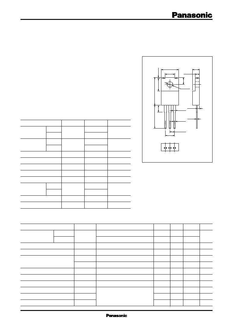
Unit: mm
1:Base
2:Collector
3:Emitter
TO≠220 Full Pack Package(a)
10.0
±
0.2
5.5
±
0.2
7.5
±
0.2
16.7
±
0.3
0.7
±
0.1
14.0
±
0.5
Solder Dip
4.0
0.5
+0.2
≠0.1
1.4
±
0.1
1.3
±
0.2
0.8
±
0.1
2.54
±
0.25
5.08
±
0.5
2
1
3
2.7
±
0.2
4.2
±
0.2
4.2
±
0.2
3.1
±
0.1
2
Power Transistors
2SC3970, 2SC3970A
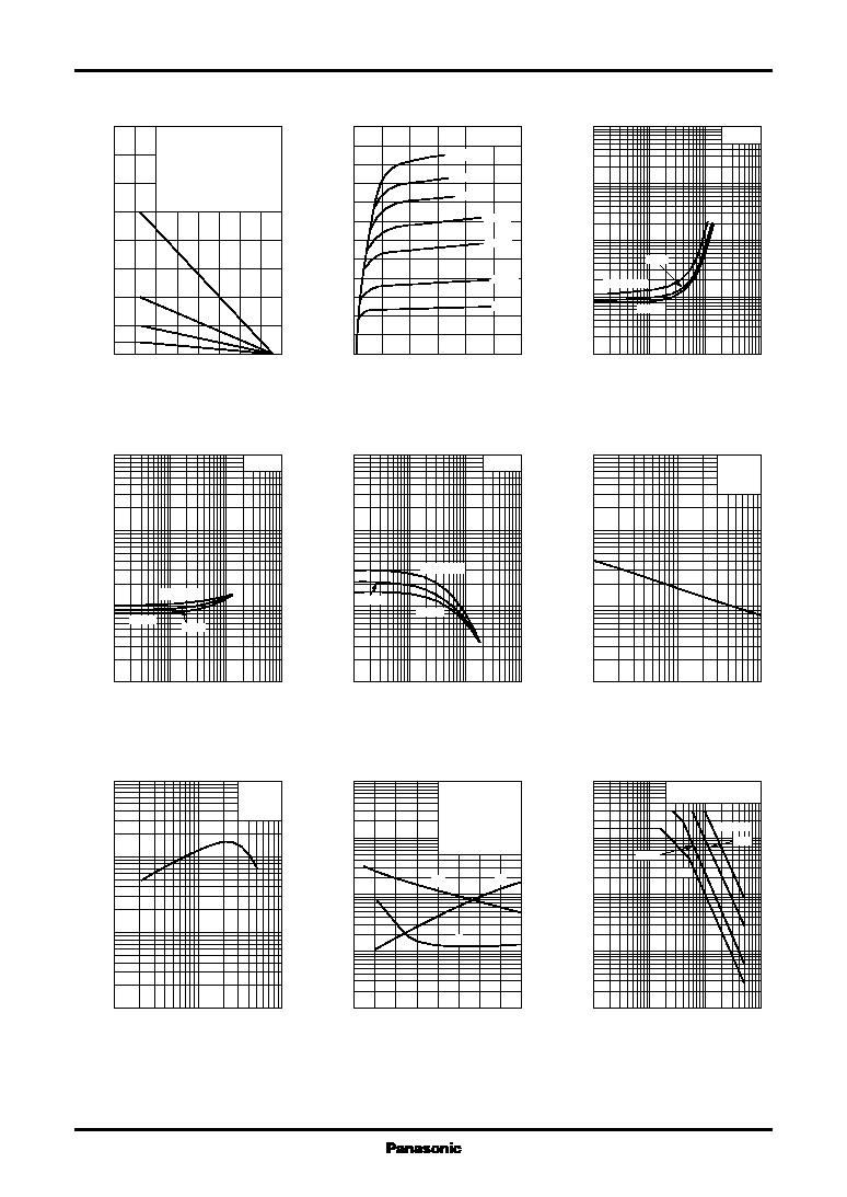
P
C
-- Ta
I
C
-- V
CE
V
CE(sat)
-- I
C
V
BE(sat)
-- I
C
h
FE
-- I
C
C
ob
-- V
CB
f
T
-- I
C
t
on
, t
stg
, t
f
-- I
C
Area of safe operation (ASO)
0
160
40
120
80
140
20
100
60
0
40
30
10
20
(1)
(3)
(4)
(2)
(1) T
C
=Ta
(2) With a 100
◊
100
◊
2mm
Al heat sink
(3) With a 50
◊
50
◊
2mm
Al heat sink
(4) Without heat sink
(P
C
=2W)
Ambient temperature Ta (∞C)
Collector power dissipation P
C
(W
)
0
12
10
8
2
6
4
0
1.2
1.0
0.8
0.6
0.4
0.2
T
C
=25∞C
100mA
80mA
60mA
40mA
20mA
10mA
I
B
=150mA
Collector to emitter voltage V
CE
(V)
Collector current I
C
(A
)
0.01
0.1
1
10
0.03
0.3
3
0.01
0.03
0.1
0.3
1
3
10
30
100
I
C
/I
B
=5
T
C
=100∞C
25∞C
≠25∞C
Collector current I
C
(A)
Collector to emitter saturation voltage V
CE(sat)
(V
)
0.01
0.1
1
10
0.03
0.3
3
0.1
100
10
1
0.3
3
30
I
C
/I
B
=5
T
C
=≠25∞C
25∞C
100∞C
Collector current I
C
(A)
Base to emitter saturation voltage V
BE(sat)
(V
)
0.01
0.1
1
10
0.03
0.3
3
1
1000
100
10
3
30
300
V
CE
=5V
≠25∞C
T
C
=100∞C
25∞C
Collector current I
C
(A)
Forward current transfer ratio h
FE
1
3
10
30
100
1
1000
100
10
3
30
300
I
E
=0
f=1MHz
T
C
=25∞C
Collector to base voltage V
CB
(V)
Collector output capacitance C
ob
(pF
)
0.01
0.03
0.1
0.3
1
0.1
100
10
1
0.3
3
30
V
CE
=10V
f=1MHz
T
C
=25∞C
Collector current I
C
(A)
Transition frequency f
T
(MHz
)
0
2.0
0.5
1.5
1.0
0.01
0.03
0.1
0.3
1
3
10
30
100
t
stg
t
f
t
on
Pulsed t
w
=1ms
Duty cycle=1%
I
C
/I
B
=3.5
(2I
B1
=≠I
B2
)
V
CC
=200V
T
C
=25∞C
Collector current I
C
(A)
Switching time t
on
,t
stg
,t
f
(
µ
s
)
1
10
100
1000
3
30
300
0.001
0.003
0.01
0.03
0.1
0.3
1
3
10
Non repetitive pulse
T
C
=25∞C
DC
10ms
1ms
t=0.5ms
Collector to emitter voltage V
CE
(V)
Collector current I
C
(A
)

3
Power Transistors
2SC3970, 2SC3970A
Area of safe operation, reverse bias ASO
Reverse bias ASO measuring circuit
R
th(t)
-- t
10
≠4
10
10
≠3
10
≠1
10
≠2
1
10
3
10
2
10
4
0.1
1
10
100
10000
1000
Note: R
th
was measured at Ta=25∞C and under natural convection.
(1) P
T
=10V
◊
0.2A (2W) and without heat sink
(2) P
T
=10V
◊
1.0A (10W) and with a 100
◊
100
◊
2mm Al heat sink
(1)
(2)
Time t (s)
Thermal resistance R
th
(t)
(∞C/W
)
0
800
200
600
400
700
100
500
300
0
4.0
3.0
1.0
2.5
3.5
2.0
0.5
1.5
L
coil
=180
µ
H
I
C
/I
B
=5
(I
B1
=≠I
B2
)
T
C
<100∞C
Collector to emitter voltage V
CE
(V)
Collector current I
C
(A
)
L coil
I
C
I
B1
V
in
t
W
≠I
B2
Vclamp
V
CC
T.U.T