 | –≠–ª–µ–∫—Ç—Ä–æ–Ω–Ω—ã–π –∫–æ–º–ø–æ–Ω–µ–Ω—Ç: AN1339S | –°–∫–∞—á–∞—Ç—å:  PDF PDF  ZIP ZIP |

s Overview
The AN1339 (AN6912N) and the AN1339S are qua-
druple (voltage) comparators with wide range of operat-
ing supply voltages.
s Features
∑ Wide range of supply voltage
Single supply:2 to 36V
Dual supply:
±
1 to
±
18V
∑ Low circuit current:0.8mA typ.
∑ Wide range of common-mode input voltages
:0V to V
CC
≠1.5V (single supply)
∑ Open collector output
AN1339 (AN6912N), AN1339S
Quadruple Comparators
s Block Diagram
1
2
3
4
5
6
7
14
13
12
11
10
9
8
19.06
±
0.3
3--15∞
Unit:mm
AN1339 (AN6912N)
6.35
±
0.3
0.5
±
0.1
1.22
±
0.25
2.54
3.05
±
0.25
4.7
±
0.25
7.62
±
0.25
0.3
+ 0.1
≠ 0.05
1.1
±
0.25
14-pin DIL Plastic Package (DIP014-P-0300D)
Unit:mm
AN1339S
1.24
0.4
±
0.25
1.27
0.1
±
0.1
0.3
1.5
±
0.2
0.45
0.15
1
2
3
4
5
6
7
14
13
12
11
10
9
8
6.5
±
0.3
4.2
±
0.3
10.1
±
0.3
14-pin PANAFLAT Plastic Package (SOP014-P-0225A)
D
11
D
10
D
9
D
8
D
7
D
6
D
5
D
4
D
2
D
1
D
3
R
1
V
in2
V
CC
Q
10
Q
8
Q
6
Q
4
Q
3
Q
1
Q
55
Q
11
Q
12
Q
16
Q
17
Q
22
Q
24
Q
20
Q
18
Q
19
Q
21
Q
27
Q
26
Q
32
Q
34
Q
30
Q
28
Q
29
Q
31
Q
37
Q
36
Q
42
Q
44
Q
40
Q
38
Q
39
Q
41
Q
54
Q
51
Q
50
Q
52
Q
48
Q
47
Q
46
Q
49
Q
9
Q
7
Q
5
Q
2
V
in4
≠
V
in3
≠
V
in1
≠
V
in2
≠
V
O4
V
O1
V
O1
V
O2
V
EE
(GND)
V
in1
+
V
in3
+
V
in4
+
1
6
2
4
14
8
13
10
12
11
9
5
3
7
s Pin Descriptions
Pin No.
Pin name
1
2
3
4
5
6
7
Ch.2 output
Ch.1 output
V
CC
Ch.1 inverting input
Ch.1 non inverting input
Ch.2 inverting input
Ch.2 non inverting input
Pin No.
Pin name
8
9
10
11
12
13
14
Ch.3 inverting input
Ch.3 non inverting input
Ch.4 inverting input
Ch.4 non inverting input
V
EE
(GND)
Ch.4 output
Ch.3 output
V
CC
V
ICM
*
1
V
ID
*
2
P
D
T
opr
T
stg
V
V
V
mW
∞C
∞C
Parameter
Symbol
Rating
Unit
s Absolute Maximum Ratings (Ta=25∞C)
36
≠0.3 to +36
36
570
380
≠30 to +85
≠55 to +150
≠55 to +125
Voltage
Power dissipation
Operating ambient temperature
Storage
temperature
Supply voltage
Common-mode input voltage
Differential input voltage
AN1339 (AN6912N)
AN1339S
AN1339 (AN6912N)
AN1339S
*1 The common mode input voltage is a voltage applied to the non-inverting input pin and inverting input pin simultaneously.
*2 Differential input is equivalent to the potential difference between the non-inverting input pin and inverting input pin.
Parameter
Symbol
Condition
min
typ
max
Unit
s Electrical Characteristics (V
CC
=5V, Ta=25
±
2∞C)
Input offset voltage
V
I (offset)
5
mV
2
Input offset current
I
IO
50
nA
Input bias current
I
Bias
250
nA
Voltage gain
G
V
V/mV
R
L
=15k
R
L
=
R
L
=5.1k
, V
RL
=5V
Common-mode input voltage range
0
V
CM
V
CC
≠1.5
V
Supply current
I
CC
2
mA
1.1
Response time
t
r
µ
s
1.3
200
Output sink current
10
I
SINK
mA
V
REF
=0V, V
IN
=1V, V
O
1.5V
Low-level output voltage
V
OL
0.4
V
0.2
V
REF
=0V, V
IN
=1V, I
SINK
=3mA
Output terminal leakage current
I
O (Leak)
nA
0.1
V
IN
=0V, V
REF
=1V, V
O
=5V
=
<
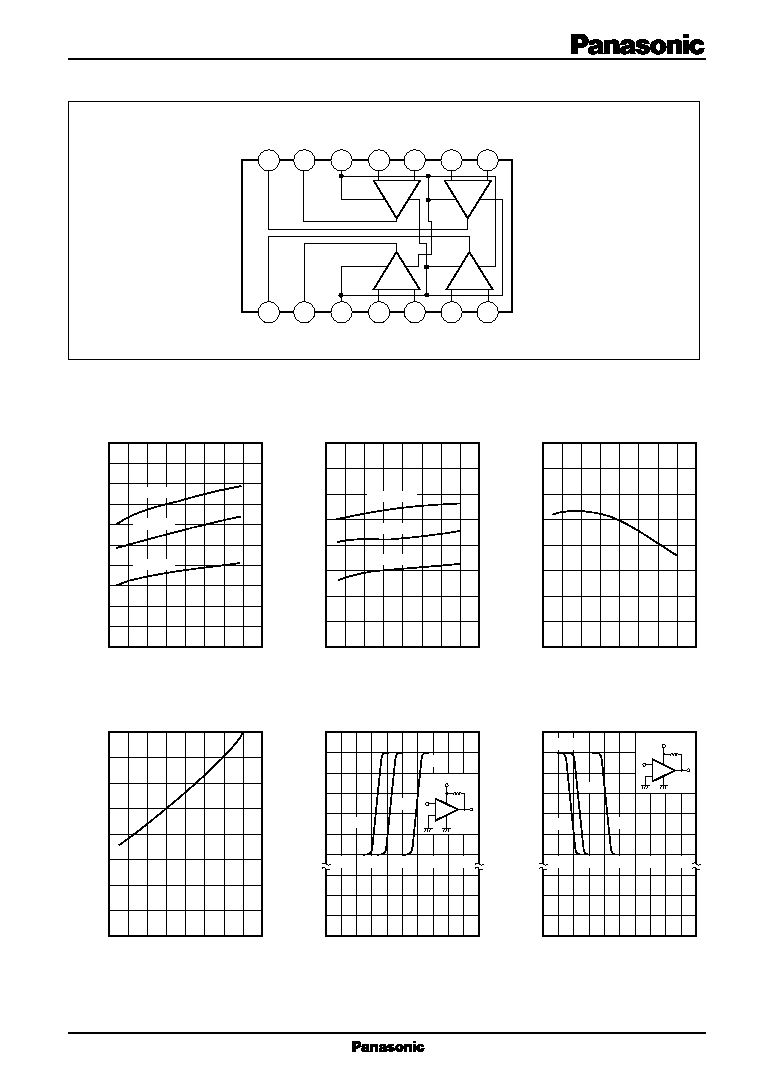
s Characteristics Curve
≠
+
+
≠
≠
+
+
≠
V
O2
V
CC
1
2
3
4
5
6
7
14
4
3
1
2
13
12
11
V
EE
10
9
8
V
in1
+
V
in1
≠
V
O1
V
in2
≠
V
in2
+
V
O3
(GND)
V
in4
+
V
in3
+
V
in4
≠
V
O4
V
in3
≠
VCC=5V
VO
VIN
1k
+
≠
2.0
1.8
1.6
1.4
1.2
1.0
0.8
0.6
0.4
0.2
0
0
10
20
30
40
Supply Voltage V
CC
(V)
Supply Current I
CC
(mA)
I
CC
≠V
CC
Ta=≠10∞C
Ta=25∞C
Ta=70∞C
Supply Voltage V
CC
(V)
80
70
60
50
40
30
20
10
0
Input Bias Current I
Bias
(nA)
I
Bias
≠V
CC
0
10
20
30
40
Ambient Temperature Ta (∞C)
32
28
24
20
16
12
8
4
0
Output Sink Current I
SINK
(mA)
I
SINK
≠Ta
≠40
0
40
80
120
Ambient Temperature Ta (∞C)
0.32
0.28
0.24
0.20
0.16
0.14
0.12
0.04
0
Output Saturation Voltage Level V
OL
(V)
V
OH
≠Ta
≠40
0
40
80
120
Time t (
µ
s)
6
5
4
3
2
1
0
100
50
0
Input Voltage V
IN
(mV)
Output Voltage V
O
(V)
Transfer Characteristics (1)
0
0.5
1.0
1.5
2.0
Time t (
µ
s)
6
5
4
3
2
1
0
0
≠50
≠100
Input Voltage V
IN
(mV)
Output Voltage V
O
(V)
Transfer Characteristics (2)
0
0.5
1.0
1.5
2.0
V
CC
=5V
V
O
V
IN
1k
+
≠
V
CC
=5V
V
O
V
IN
5.1k
+
≠
5mV
20mV
60mV
60mV
20mV
5mV
Overdrive
Ta=≠10∞C
Ta=25∞C
Ta=70∞C
s Block Diagram