 | –≠–ª–µ–∫—Ç—Ä–æ–Ω–Ω—ã–π –∫–æ–º–ø–æ–Ω–µ–Ω—Ç: AN1431T | –°–∫–∞—á–∞—Ç—å:  PDF PDF  ZIP ZIP |

s Overview
The AN1431T and AN1431M are high accuracy stabilized
power supplies in which the output voltage can be adjusted in
the range from approx. 2.5 to 36V by using the external resistor
under the operating temperature. Because of its fast rise charac-
teristics, it can be replaced with Zener diode and has the wide
application range.
s Features
∑
High precision reference voltage : 2.5V±2%
∑
High-temperature stability : 17ppm/∞C typ.
∑
Output voltage externally adjustable : 2.5 to 36V
∑
Fast rise
∑
Low input impedance : 0.2
(typ.)
∑
Low output noise voltage
AN1431T, AN1431M
Surface-mount Adjustable Output Shunt Regulator
Unit : mm
AN1431T
JEDEC : TO-92 (SSIP003-P-0000)
5.0
±
0.2
5.1
±
0.2
13.5
±
0.5
0.45
2.3
±
0.2
2.54
3
2
1
+ 0.2
≠ 0.1
4.0
±
0.2
1
3
2
1
3
2
≠
Error
Amp.
+
Current
Source
Voltage
Reference
Output Tr
I
K
V
1
R
1
R
2
R
1
R
2
I
REF
V
REF
V
KA
V
KA
= V
REF
(1 + ) + I
REF
∑ R
1
R
2
= 2.5k
Pin number in is for the AN1431T.
Pin number in is for the AN1431M.
s Block Diagram
Unit : mm
AN1431M
JEDEC : TO-92 (SSIP003-P-0000)
5.0
±
0.2
5.1
±
0.2
13.5
±
0.5
0.45
2.3
±
0.2
2.54
3
2
1
+ 0.2
≠ 0.1
4.0
±
0.2
s Pin Name
AN1431T
Pin No.
Pin name
1
2
3
Cathode
Reference pin
Anode
AN1431M
Pin No.
Pin name
1
2
3
Reference pin
Anode
Cathode
V
CC
I
CC
P
D
I
REF
V
opr
T
stg
V
mA
mW
mA
∞C
∞C
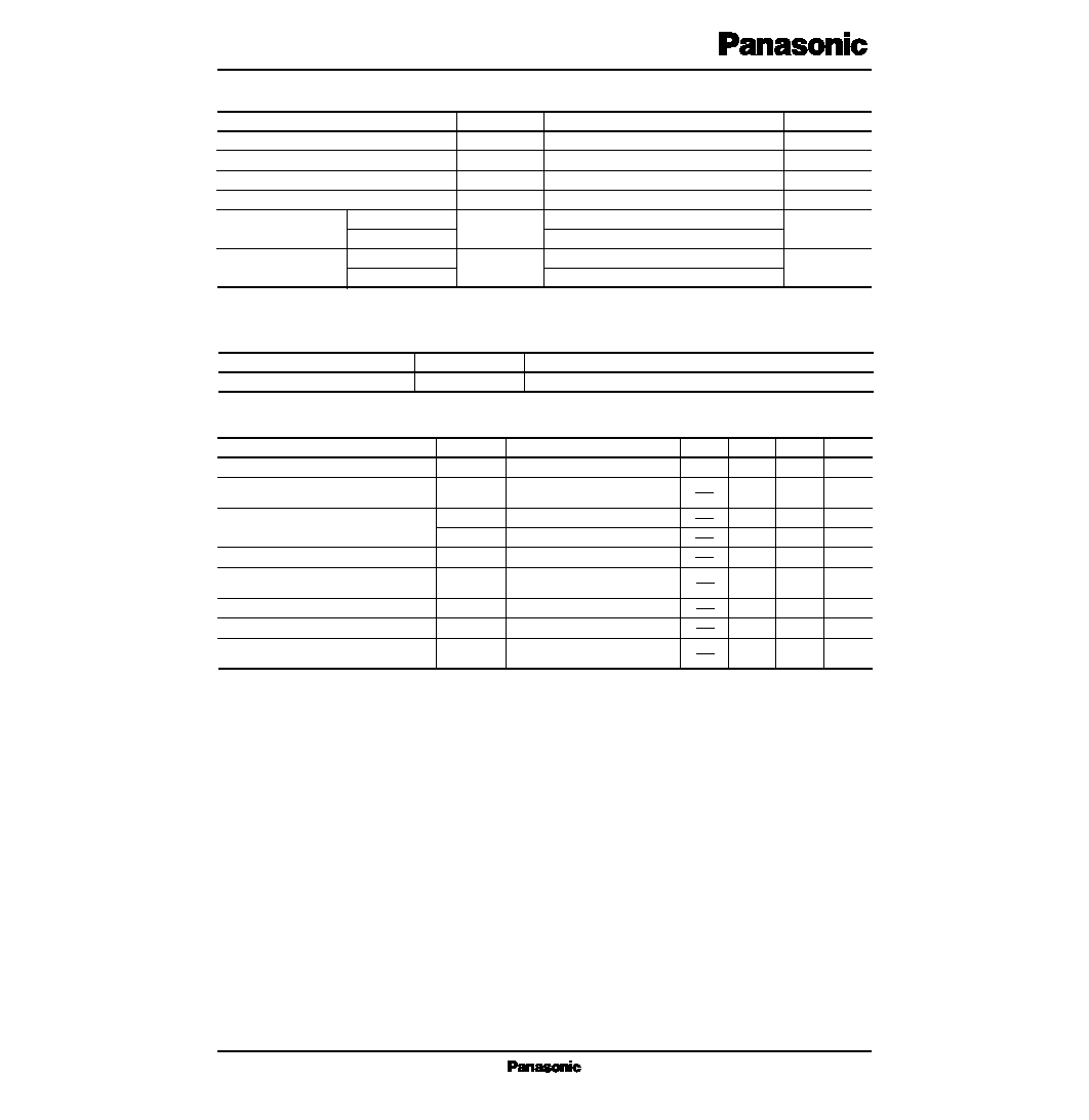
s Absolute Maximum Ratings (Ta=25∞C)
37
≠100 to+150
650 *
≠ 0.05 to+10
≠20 to+85
≠25 to+80
≠55 to+150
≠55 to+125
Supply voltage
Supply current
Power dissipation
Reference input current
Operating ambient
temperature
Storage temperature
AN1431T
AN1431M
AN1431T
AN1431M
* For the AN1431M, SM to the printed board (glass epoxy of 20
◊
20
◊
1.7mm with copper film of 1cm
2
)
Parameter
Symbol
Rating
Unit
Parameter
Symbol
Range
s Recommended Operating Range (Ta=25∞C)
Operating supply voltage range
V
KA
V
REF
(2.5 to 36V)
Reference voltage
V
REF
2.55
V
2.50
V
KA
=V
REF
, I
K
=10mA
V
KA
=V
REF
, I
K
=10mA,
Ta=0 to+70∞C
Reference voltage fluctuation
V
REF
≠2.7
mV/V
≠1.2
I
K
=10mA, DV
KA
=10V to V
REF
V
KA
mV/V
I
K
=10mA, DV
KA
=36 to 10V
Reference input current
I
REF
µ
A
2
I
K
=10mA, R
1
=10k
, R
2
=
µ
A
I
K
=10mA, R
1
=10k
, R
2
=
,
Ta=0 to+70∞C
Reference input current temperature deviation
I
REF (Jev)
*
2
mA
0.4
V
KA
=V
REF
≠1
Minimum cathode current
I
min
µ
A
0.1
V
KA
=36V, V
REF
=0V
Off-state cathode current
I
OFF
Dynamic impedance
|Z
KA
| *
3
V
KA
=V
REF
, I
K
=1 to 100mA,
f 1kHz
1.0
0.5
≠2
4
1.2
1.0
2.45
Reference voltage temperature deviation
V
REF (Jev)
*
1
*
2
mV
3
17
0.4
0.2
Parameter
Symbol
Condition
min
typ
max
Unit
s Electrical Characteristics (Ta=25∞C)
<
=
V
REF
*1
V
REF (max)
V
REF (min)
V
REF (dev)
= V
REF (max)
≠V
REF (min)
V
REF (dev)
V
REF (max)
=2500mV (Ta=30∞C),
V
REF (min)
=2497mV (Ta=0∞C),
(V
REF (dev)
=3mV),
V
REF
=2499mV (Ta=25∞C)
Ta=70∞C
Ta
Ta
I
REF
I
REF (max)
I
REF (min)
I
REF (dev)
= I
REF (max)
≠ I
REF (min)
I
REF (dev)
Ta
|aV
REF
|=
◊
10
6
(ppm/∞C)
V
REF
*
V
REF (dev)
70∞C
|aV
REF
| =
◊
10
6
=17.1 (ppm/∞C)
|Z
KA
| =
2499mV
I
K
V
KA
|Z| = = |Z
KA
|
1 +
I
V
R
2
R
1
3mV
*
V
REF
at Ta=25∞C
For example, assuming the following ;
Then, the following expression is established.
*2 These values are design reference values, not
guaranteed ones.
*3 The dynamic impedance is defined by the following
expression.
The total dynamic impedance at
V
REF
,
V
KA
,
I
REF
, and I
REF (dev)
is as follows.
The temperature coefficient aV
REF
for the reference input
voltage is equivalently given by the following expression.
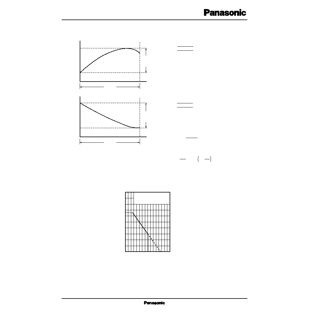
1000
900
800
700
600
500
400
300
200
100
0
0
20
40
60
80 100 120 140 160
Ambient Temperature Ta (∞C)
P
o
w
e
r
D
i
s
s
i
p
a
t
i
o
n
P
D
(
m
W
)
P
D
≠ Ta
Mounting onto Substrate :
20
◊
20
◊
1.7mm Glass Epoxy
Substrate, Copper Foil 1cm
2
or More
s Power Dissipation
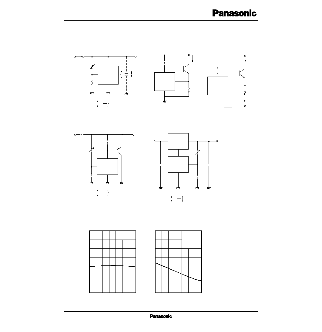
V
O
C
O
C
I
+V
AN1431T/M
1.Shunt Regulator
4.Current Boost
5.Adjustable Output Regulator Combined
with 3-pin Regulator
2.Constant Current Power
Supply
3.Constant Current Source
AN1431T/M
I
O
I
O
V
O
R
1
V
REF
R
2
R
S
R
S
+V
+V
+V
V
O
+V
R
1
V
REF
R
2
R
1
V
REF
R
2
AN1431T/M
AN7805
AN1431T/M
AN1431T/M
V
O
= 1+ V
REF
R
1
R
2
I
O
=
V
REF
R
S
I
O
=
V
REF
R
S
V
O
= 1+ V
REF
R
1
R
2
V
O
= V
REF
1+ V
O (min)
= V
REF
+ 5V
R
1
R
2
s Application Circuits
2700
2650
2600
2550
2500
2450
2400
2350
≠50
≠25
0
25
50
75
100
125
Ambient Temperature Ta (∞C)
R
e
f
e
r
e
n
c
e
V
o
l
t
a
g
e
V
R
E
F
(
m
V
)
V
REF
≠ Ta
V
K
=V
REF
I
K
=10mA
4
3
2
1
≠40
≠20
0
20
40
60
80
100
Ambient Temperature Ta (∞C)
R
e
f
e
r
e
n
c
e
I
n
p
u
t
C
u
r
r
e
n
t
I
R
E
F
(
µ
A
)
I
REF
≠ Ta
I
K
=10mA
R
1
=10k
R
2
=
s Characteristics Curve