 | –≠–ª–µ–∫—Ç—Ä–æ–Ω–Ω—ã–π –∫–æ–º–ø–æ–Ω–µ–Ω—Ç: AN2018 | –°–∫–∞—á–∞—Ç—å:  PDF PDF  ZIP ZIP |
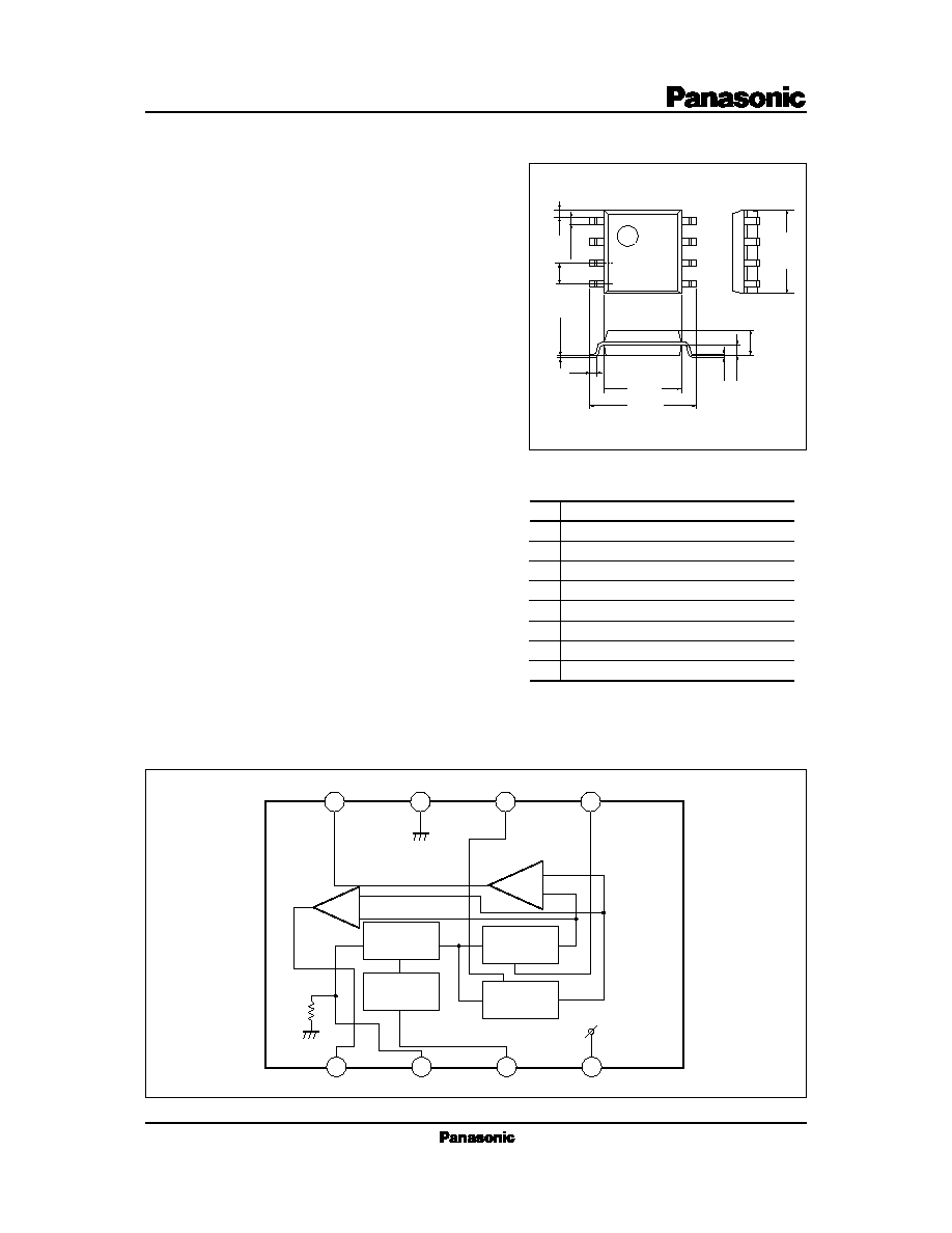
s Block Diagram
AN2018S
Correlated Double Sampling IC
s Overview
The AN2018S is used to reduce noise in CCD im-
age sensor output signal. It performs correlated double-
sampling on image signal sent from a CCD sensor to
output clearer image signal.
s Features
∑ Operating on low voltage (V
CC
=4.8V), consuming
little current (I
CC
=12.7mA typ.)
∑ Including a high-speed sampling circuit responding
to 510-830H CCD
∑ 6dB or 9dB fixed gain
∑ 83-dB high S/N-ratio (at 6dB output)
8
7
6
5
1
2
3
4
6dB OUT
GND
SP1
SP2
9dB OUT
BLK
SIG.IN
V
CC
9dB
6dB
S / H
S / H
BLK
BIAS
+
≠
50k
+
≠
CDS output (9dB)
Blanking pulse input
CCD signal input
V
CC
Sampling pulse input (2)
Sampling pulse input (1)
GND
CDS output (6dB)
Pin No.
1
2
3
4
5
Pin name
6
7
8
p
s Pin Descriptions
Unit:mm
6.5
±
0.3
4.2
±
0.3
0.4
±
0.25
0.4
1.27
0.1
±
0.1
0.15
0.65
1.5
±
0.2
5.0
±
0.3
0.3
8-Pin SOP Package (SOP008-P-0225)

Parameter
Symbol
Rating
Unit
V
CC
I
CC
P
D
T
opr
T
stg
Supply voltage
Supply current
Power dissipation
Operating ambient temperature
Note 1)
Storage temperature
Note 1)
Note 1) Ta=25∞C except operating ambient temperature and storage temperature.
5.5
18
99
≠20 to +70
≠55 to +125
V
mA
mW
∞C
∞C
s Absolute Maximum Ratings
16.2
mA
I
CC
V
3
V
8
V
1
G
1
Supply current
Terminal voltage pin (8)
Terminal voltage pin (1)
6dB amp. gain
V
dB
dB
Parameter
min
Condition
typ
max
Unit
Symbol
Note) The value in the above characteristics is not a guaranteed value, but reference one on design.
* The characteristics are of the amplifier itself.
9dB amp. gain
G
2
9.2
V
V
2.78
1.90
1.85
7.0
10.2
12.7
2.63
1.60
1.55
6.0
9.0
2.48
1.30
1.25
5.0
7.8
V
CC
=4.8V
V
CC
=4.8V
Pint, y=4.8V
Input level=300mV
P
≠
P
Input level=300mV
P
≠
P
Terminal voltage pin (3)
AMP frequency characteristics *
AMP common mode
rejection ratio *
Sampling pulse threshold (1)
Sampling pulse threshold (2)
Blanking pulse high level
f
C
CMR
V
THB
V
TH1
V
TH2
V
CC
=4.8V
V
3
=100mV
P
≠
P
10MHz
V
CC
=4.8V
V
3
=100mV
P
≠
P
10MHz
V
CC
=4.8V
V
CC
=4.8V
V
CC
=4.8V
V
3
=300mV
P
≠
P
0.8
0.8
3.5
≠3.0
≠35
1.5
1.5
2.2
2.2
dB
dB
V
V
V
s Electrical Characteristics (V
CC
=4.8V, Ta=25
±
2∞C)
V
CC
=4.8V
Pint, y=4.8V
V
CC
=4.8V
Pint, y=4.8V
Parameter
Symbol
Range
Operating supply voltage range
V
CC
4.5V to 5.1V
sRecommended Operating Range (Ta=25∞C)

Note) The above characteristics value, measured at V
CC
=5V, is not a guaranteed value, but reference one on design.
Pin No.
Pin name
Equivalent circuit
1
9dB OUT
V
CC
(4)
DC voltage (V
CC=
5V)
Description
2
3
4
BLK
SIG.IN
SP2
1k
H 3.5V
Black level:
1.55V
50k
50
µ
A
5
s Pin Descriptions
6
7
8
L 0.5V
Black level:
2.6V
V
CC
4.8V
H 2.2V
L 0.8V
SP1
H 2.2V
L 0.8V
GND
6dB OUT
Black level:
1.6V
Same as for Pinq.
1
3
5
6
GND
(7)
1k
63k
33k
V
CC
(4)
75
µ
A
200
1k
58k
500
38k
300
µ
A
300
µ
A
1k
1k
28k
20k
28k
20k
8
GND (7)
V
CC
(4)
GND (7)
V
CC
(4)
GND (7)
V
CC
(4)
GND (7)
∑9-dB-amp. output CDS signal
∑Typical 1.55V DC output
∑90-
output impedance
∑Blanking (Hclear) pulse input (from
an AN2145 series only)
∑Active high
∑3.0V threshold voltage
∑50k
input impedance
∑Grounded or left open when not
used
∑CCD signal input
∑CCD signal must be input through
a capacitor.
∑The capacitor should preferably be
0.022
µ
F.
∑2.6V typ. bias voltage
∑Sample-hold pulse input
∑Active high
∑1.5V threshold voltage
∑Sampling pulses are input in syn-
chronization with the video timing
of CCD signal at Pine.
∑Sample-hold pulse input
∑Active high
∑1.5V threshold voltage
∑Sampling pulses are input in syn-
chronization with the feed-through
timing of CCD signal at Pine.
∑Supply voltage
∑Ground
∑6-dB-amp. output CDS signal