s Overview
The AN6448NFBP is a speech network IC suitable for multi-
function cordless telephones. It incorporates a cross-point
switch controlled by serial input. It allows speech path switch-
ing and mixing, and provides for three- or four-person commu-
nication and other sophisticated functions. It also incorporates
REC/PLAY amplifiers with VOX circuits.
s Features
∑
The speech block can operate on line voltage, with no exter-
nal power supply, and is operational even during a commer-
cial power failure.
∑
Incorporates auto. PAD, dial mute, DC voltage regulation,
and other basic speech functions.
∑
The cross-point switch can be operated independently.
∑
Each output of the cross-point switch can correspond to mul-
tiple inputs, allowing three-or four-person communication.
∑
The REC/PLAY amplifiers incorporate ALC and VOX circuits.
∑
Receiver volume can be increased by 6 dB or 9 dB.
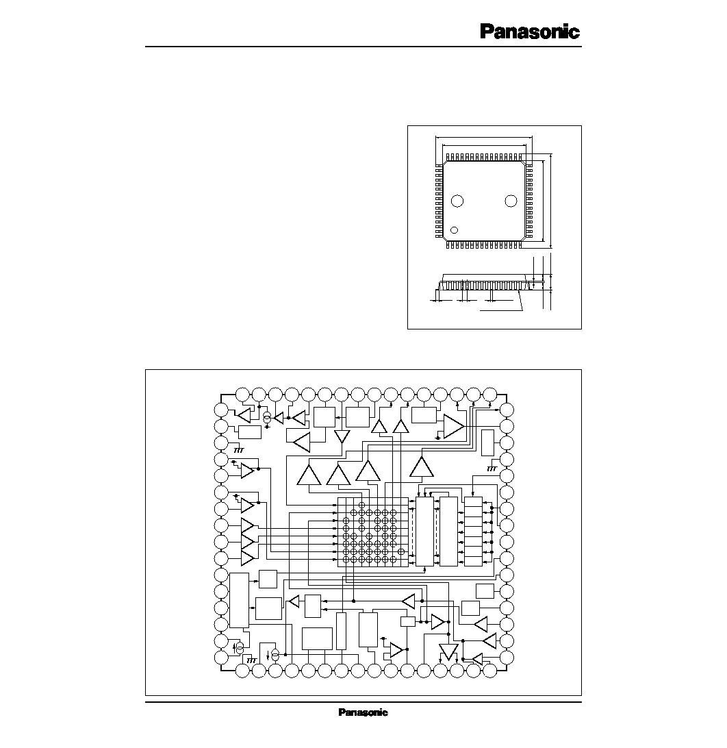
AN6448NFBP
Speech Network IC Incorporating Cross-Point Switch
Unit : mm
QFP package with 64 pins (QFH064-P-1414A)
17.2
±
0.4
14.0
±
0.3
17.2
±
0.4
14.0
±
0.3
48
33
1
16
17
32
64
49
2.85
±
0.2
1.3
±
0.1
1.3
±
0.1
0.1
±
0.1
0.2
+0.1 -0.05
0.35
+0.1
-0.05
0.8
(0.8)
SEATING PLANE
32
31
30
29
28
27
26
25
24
23
22
21
20
19
18
17
16
1
2
3
4
5
6
7
8
9
10
11
12
13
14
15
10dB
0/12
dB
20
dB
18
dB
18
dB
Comp
0dB
0dB
0dB
0dB
0dB
0dB
0dB
0dB
0dB
0dB
≠
+
≠
+
≠
+
≠
+
≠
+
V
REF
≠
+
VOX
Det.
I
N
J
ACL
Det
ACL
Line
Supply
Monitor
Hold off
Latch
Decoder
Power Supply
Control
V
REF
AP
AP
AP
Cont.
DM
Cont.
DC
Cont.
D
a
1
a
2
a
3
a
4
a
5
a
6
49
50
51
52
53
54
55
56
57
58
59
60
61
62
63
64
20
dB
33
48
47
46
45
44
43
42
41
40
39
38
37
36
35
34
P.O.R
s Block Diagram

V
CC
I
CC
V
L
I
L
P
D
T
opr
T
stg
Supply voltage (1)
Supply current (1)
Supply voltage (2)
Supply current (2)
Power dissipation
Note)
Operating ambient temperature
Storage temperature
V
mA
V
mA
mW
∞C
∞C
s Absolute Maximum Ratings (Ta=25∞C)
7.0
50
12.0
135
640
≠20 to +75
≠55 to +150
Note) In a free-air condition with Ta=75∞C.
Parameter
Symbol
Rating
Unit
s Recommended Operating Conditions (Ta=25∞C)
Operating supply voltage range (1)
Operating supply voltage range (2)
Clock frequency
V
CC
V
L
f
CLK
4.5
3
5
5.5
11
250
V
V
kHz
Parameter
Symbol
Condition
min
typ
max
Unit
s Electrical Characteristics (Ta=25∞C)
Speech network block
Rec. gain
G
V
≠ER1
34.5
dB
I
L
=30mA, V
CC
=5V,
Vin=≠42dBm
30.5
32.5
Rec. automatic PAD width
AP≠ER
5
dB
I
L
=30 to 80mA, V
CC
=5V,
Vin=≠42dBm
2.5
3.7
Trans. gain
G
V
≠EM1
31.7
dB
I
L
=30mA, V
CC
=5V,
Vin=≠38dBm
27.7
29.7
Trans. automatic PAD width
AP≠EM
5
dB
I
L
=30 to 80mA, V
CC
=5V,
Vin=≠38dBm
2.5
4
DTMF gain
G
V
≠ED1
20.9
dB
I
L
=30mA, V
CC
=5V,
DM=ON, Vin=≠30dBm
I
L
=30 to 80mA, V
CC
=5V,
V≠DMC=LOW,
Vin=≠30dBm
16.9
18.9
DTMF automatic PAD width
AP≠EDT
5.5
dB
2.5
4.1
REC/PLAY amp. block
Switch block
Head bias current
145
I≠REC
µ
A
180
215
REC preamp. output
≠13.4
V
O
≠RP
dBm
Vin=≠45dBm, Rin=10k
≠11.4
≠9.4
EQ amp. gain
27.8
G
V
≠EQ
dB
Vin=≠40dBm
29.8
31.8
SP out max output
0
V
O
≠SP
dBm
Input L-SP IN, THD=5%
4
DH out max output
0
V
O
≠DH
dBm
Input RF1 IN, THD=5%
4
RF1 out max output
0
V
O
≠RF1
dBm
Input RF2 IN, THD=5%
4
RF2 out max output
0
V
O
≠RF2
dBm
Input RF1 IN, THD=5%
4
L-REC out max output
0
V
O
≠LR
dBm
Input AUX IN, THD=5%
4
Parameter
Symbol
Condition
min
typ
max
Unit
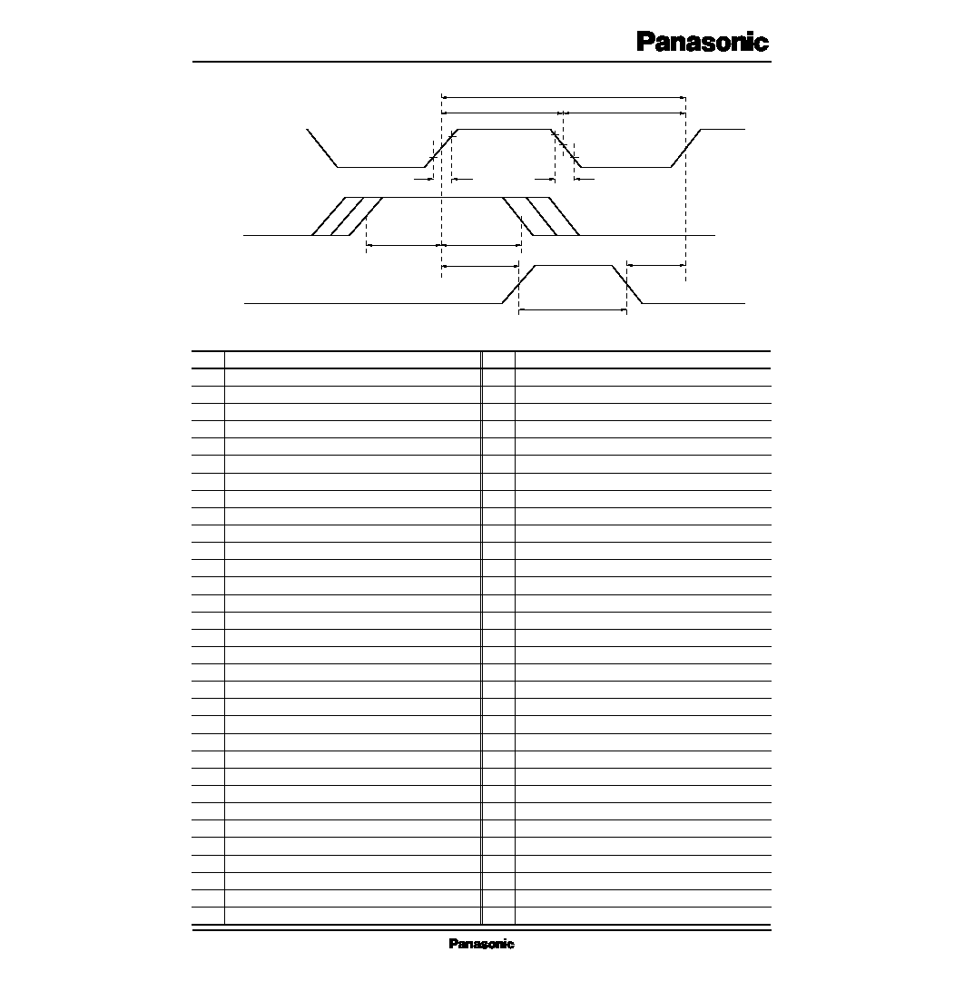
s Timing Chart
CLK
DATA
STR
1/f
CLK
t
wh (CLK)
90%
10%
10%
2.5V
90%
2.5V
2.5V
2.5V
2.5V
2.5V
2.5V
t
WL (CLK)
t
r (CLK)
t
f (CLK)
t
su (DATA)
t
h (DATA)
t
su (STB)
t
sr (STB)
t
W (STB)
s Pin Descriptions
Pin No.
Description
1
2
3
4
5
6
7
8
9
10
11
12
13
14
15
16
17
18
19
20
21
22
23
24
25
26
27
28
29
30
31
32
Ground
Line power (+) input
Side-tone adjustment
Line voltage control (1)
Int. ref. voltage output (1)
Int. ref. voltage output (2)
Hold-reset control
Trans. preamp. output
Auto. PAD control
Rec. preamp. input
Rec. preamp. output
Rec. amp. input
Rec. amp. output (1)
Rec. amp. output (2)
MIC preamp. output
MIC preamp. input (1)
MIC preamp. input (2)
DTMF signal input
BT signal input
Dial mute control
Line voltage control
Line interruption detector output
Hold-reset signal output
No connection
Strobe signal input
Clock signal input
No connection
Data input
Ground
Logic power supply input
VOX detector output
SP link output
Pin No.
Description
33
34
35
36
37
38
39
40
41
42
43
44
45
46
47
48
49
50
51
52
53
54
55
56
57
58
59
60
61
62
63
64
RF2 link output
RF1 link output
Intercom link output
VOX detection control
VOX amp. input
Time stamp link output
Recording link output
ALC input
ALC detection control
Loudspeaker link input
Recording input
Recording inverse input
Recording preamp. output
Recording bias current control
To recording head
EQ amp. inverse input
EQ amp. output
REC/PLAY int. ref. voltage output
Ground
MIX preamp. output
MIX link input
AUX preamp. output
AUX link input
Intercom link input
RF1 link input
RF2 link input
Power-ON reset control
External supply voltage input
Internal supply voltage output
Circuit voltage control (2)
Line current bypass (2)
Line current bypass (1)

s Pin Descriptions
1 GND
2 V
L
I
3
ST
V
L
≠
CONT
I
O
4
V
REF
≠
SN
HCO
HCC
APC
Vreg-R ∑ I
I
L
T≠
FILTER
5 V
REF
O
O
O
I
I
O
O
O
6
7
23
8
9
10 RV IN
RV
PRE≠
OUT
RV
FILTER
RV
OUT
(1)
RV
OUT
(2)
11
12
13
∑
14
Description
Waveform
Remarks
PinNo. Symbol
I/O
Equivalent Circuit
TO
2
3
62
7
30k
120k
+
≠
+
≠
23
4
8
6k
9
I
I
L
I
10
11
+
≠
+
≠
10k
11
13
14
12
61
5
6
24k
24
k
Vreg
+
≠
+
≠
0V
DC
3 to 10V
DC
0.3V
DC1V
1V
(Const)
1V
(Const)
I
L
DC1V
V
REF
V
REF
V
REF
V
REF
V
REF
V
CC
0V
Hold-reset signal
Ground :
∑ This is the ground pin for the
speech network.
GND for REC/PLY, VRER
SPEECH and LINK.
Side-tone adjustment :
∑ Grounded through R1 (27
).
∑ Connects to the side-tone adjust-
ing circuit to adjust side tone and
receiver level.
Int. ref. voltage output (1) :
∑ Outputs half the Vreg reference
voltage.
∑ Grounded through a 0.01
µ
F
capacitor.
Line voltage control (1) :
C
2
and the internal resistance
determine the f. characteristics.
The larger the capacitance
of C10, the lower the high
band gain as with a LPF.
The larger the capacitance of
C
5
, the wider the pulse width.
C6 and the 6-k
internal
resistance as illustrated on the
left form a low-pass filter.
The receiver preamplifier
gain (G) is :
The line drive gain (G) is :
Z
Line
//Z
Tel
R
1
Also assuming
Z
Line
600
Z
Tel
600
R
1
=27
:
G=20log =20.9dB
Int. ref. voltage output (2) :
∑ Output impedance=50
Line power input :
∑ Connects to the positive output
of the diode bridge.
Hold-reset control :
∑ Grounded through C5. Adjusts
the output time of control sig-
nals.
Hold-reset signal output :
∑ This is an open-collector out-
put to a microprocessor.
∑ Requires a pull-up resistor.
Trans. preamp. output :
∑ C
6
as connected between this pin
and the ground forms a low-pass
filter.
Auto. PAD control :
∑ Connects through a resistance to
Pin61 (Vreg). If the resistance
increases, the PAD operates
closer to the near end. If the
resistance decreases, the PAD
operates closer to the far end.
Rec. preamp. input :
∑ Receiver signals are input from
the side-tone circuit to this pin.
∑ R7 and C8 connected between
Pin11 and this pin determine
Rec. preamp. output :
∑ R7 and C8 connected between
Pin10 and this pin determine
the f. characteristics.
∑ The output impedance is 100
±
50
.
Rec. amp. outputs (1 and 2) :
∑ A ceramic or dynamic receiv-
er is connected.
∑ The output circuit is a BTL con-
figuration.
∑ The output impedance is 50
±
30
.
Rec. amp. input :
27
300
G= ≠20log
R7
+
C8
1
C9
R6 +
1
1
G =

s Pin Descriptions (cont.)
15 MIC
OUT
16
O
MIC
IN
(+)
MIC
IN
(≠)
I
I
17
18
MF≠
IN
BT≠
IN
DMC
DC≠
CONT
I
I
I
O
I
I
I
19
20
21
22 CPC
NC
STR
CLK
NC
24
25
26
27
MIC preamp. input (1) :
∑ A bias resistor and a microphone
connect to this pin.
MIC preamp. output :
∑ R11 and C13 connected
between Pin17 and this pin
determine the f. characteristics.
∑ The output impedance is 300
±
100
.
Feedback is input to this pin
through a capacitor. The
capacitor and R9 to R11, and
C12 and C13 determine the f.
characteristics.
The input impedance (10k
)
and C14 or C15 form an
input HPF.
∑ Referring to the left figure, the
voltage, VCPC, at which
T
rCPC
turns ON is calculated
as follows:
V
CPC
(ON)
DTMF signal input :
∑ DTMF signals are input through
a coupling capacitor C14.
∑ When DMC is low at Pin20,
DTMF is enabled.
∑ Input impedance is 10k
.
Dial mute control :
∑ Normal speech mode when Pin20
is high or open (MIC amp. ON
and rec. amp. ON).
∑ DTMF mode when Pin20 is low
(DTMF amp. ON and BT amp.
ON).
Line voltage control :
∑ Line voltage is normal when this
pin is high. Line voltage increas-
es by 1 to 1.5V when this pin is
low.
Line interruption detector output :
∑ This is an open collector output
to a microprocessor, requiring a
pull-up resistor connected to the
microprocessor's power supply.
This pin goes low when line
voltage is 3.0V or more, and
goes high when 1.5V or less.
No connection
No connection
MIC preamp. input (2) :
∑ R11 and C13 connected
between Pin15 and this pin
determine the f. characteristics.
BT signal input :
∑ Beep tone (BT) signals are
input through a coupling
capacitor C15.
∑ Input impedance is 10k
.
Strobe signal input :
∑ The strobe signal for serial control
data is input to this pin. The rising
edge of the strobe signal deter-
mines the timing at which internal
control address or ON/OFF status
is validated.
Clock signal input :
∑ The clock signal for serial control
data is input to this pin. The rising
edge of the clock signal determines
the timing at which data is read.
◊
VBE (T
rCPC
)
=
= 2.5V (Ta=25∞C)
R1 + R2
R1
Description
Waveform
Remarks
PinNo. Symbol
I/O
Equivalent Circuit
17
16
10k
+
≠
V
REF
15
18
10k
V
REF
/SN
19
10k
V
REF
200k
100k
20
61
300k
V
CC
10k
26
200k
150k
21
144k
V
L
R2
R1
56k
22
2
Tr
CPC
300k
V
CC
10k
25
+
≠
+
≠
+
≠
V
REF
V
REF
With signal ON
V
REF
With signal ON
V
REF
V
CC
0.2V
Line voltage increases
V
CC
0.2V
Line interruption
5V
0V
5V
0V