ICs for Audio Common Use
s
Overview
The AN7164N is an integrated circuit designed for 47W
(V
CC
= 26.4V, 8
) output power amplifier. High power
output (BTL 47W), low distortion and low noise are real-
ized. High reliability is obtained due to same kinds of pro-
tectors built in. Furthermore, ON/OFF is enabled even if
power is supplied to power supply pin by stand-by circuit.
s
Features
∑
High output power
∑
Low distortion, low noise
∑
Low shock noise from power ON/OFF operation
∑
Incorporates stand-by circuits
∑
Incorporates protection circuits
(Temperature, Overcurrent, Load Short, Output ≠ GND
Short)
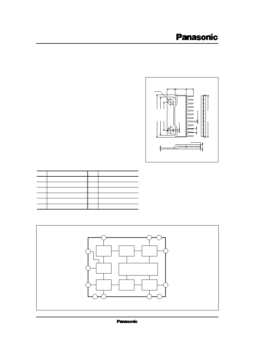
AN7164N
BTL 47W Audio Power Amplifier Circuit
2
11
12
6
1
5
3
4
8
9
7
10
V
CC
GND
GND
Input
Circuit
Driver
Circuit
Output
Circuit
Ripple
Filter
Protection
Over Temp.
Load Short
Overcurrent
Output-GND
Short
Input
Circuit
Driver
Circuit
Output
Circuit
s
Block Diagram
s
Pin Descriptions
Pin No.
Pin Name
1
2
3
4
5
6
Ripple Filter
NFB Ch.2
GND (Input)
NFB Ch.1
Input
Stand-by
Pin No.
Pin Name
7
8
9
10
11
12
Output Ch.1
Bootstrap Ch.1
GND (Output)
Output Ch.2
Bootstrap Ch.2
V
CC
29.96
±
0.3
29.6
±
0.3
12
1
Unit : mm
28.0
±
0.3
20.0
±
0.2
5.9
±
0.25 7.7
±
0.3 7.8
±
0.25
1.2
±
0.1
2.54
0.6
±
0.1
3.5
±
0.3
0.35
+ 0.1
≠ 0.05
¯ 3.6
R1.8
0.6
12-Lead SIP Package with Fin (Power Type) (HSIP012-P-000A)
ICs for Audio Common Use
AN7164N
s
Absolute Maximum Ratings
(Ta= 25∞C)
V
CC
I
CC
V
CC (surge)
P
D
T
opr
T
stg
Supply Voltage
Supply Current
Peak Supply Voltage
Power Dissipation
Operating Ambient Temperature
Storage Temperature
V
A
V
W
∞C
∞C
Parameter
Symbol
Rating
Unit
32
Note)
5
55
62.5
≠ 30 ~ + 75
≠ 55 ~ + 150
Note) Non-Signal
Parameter
Symbol
Range
s
Recommended Operating Range
(Ta= 25∞C)
Operating Supply Voltage Range
V
CC
8.3V ~ 30V
Quiescent Circuit Current
Output Noise Voltage
Output Offset Voltage
Total Harmonic Distortion
Voltage Gain
Maximum Output Power
Stand-by Current
Stand-by Threshold Voltage
I
CQ
V
no
V
O (offset)
THD
G
V
Po
I
STB
Vth
(STB)
V
in
= 0V
R
g
= 10k
Note)
V
in
= 0V
P
O
= 1W
P
O
= 1W
THD= 10%
Piny Open
DC Voltage of Piny at
I
CQ
= less than 1mA
Parameter
Symbol
Condition
min.
typ.
max.
Unit
49.5
40
55
0.9
0
0.06
51.5
47
0.1
2.7
100
1.5
300
0.3
53.5
30
mA
mV
mV
%
dB
W
µ
A
V
Note) With DIN/AUDIO filter
s
Electrical Characteristics
(V
CC
= 26.4V, R
L
= 8
, f= 1kHz, BTL Operation, Ta= 25∞C)
dB
Ripple Rejection Ratio
RR
R
g
= 0
, Supply Ripple 1Vrms,
120Hz Sine Wave
Note)
48
45
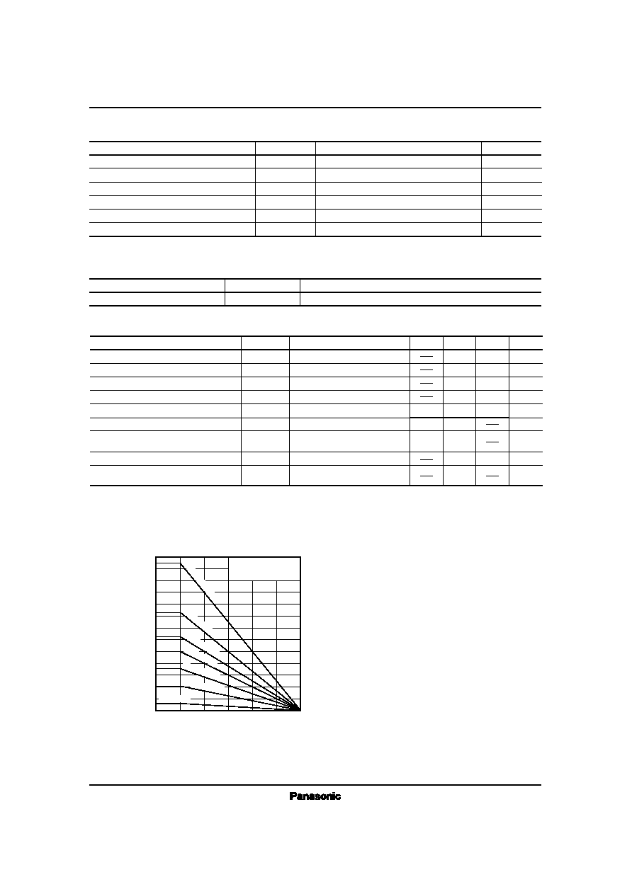
Ambient Temperature Ta (∞C)
P
o
w
e
r
D
i
s
s
i
p
a
t
i
o
n
P
D
(
W
)
50
0
25
125
75
100
150
(62.5)
s
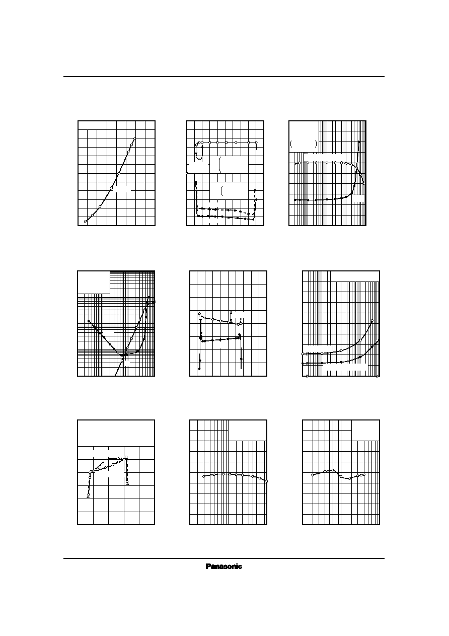
Characteristics Curve
60
50
40
30
20
10
0
(41.7)
(31.3)
(17.9)
(10.4)
(3.0)
No heat sink
10∞C/W he
at sink
5∞C/W
heat s
ink
3∞C
/W
hea
t sin
k
2∞C
/W
hea
t sin
k
1∞C
/W
he
at s
ink
(25.0)
R
th (j ≠ c)
= 2∞C/W
R
th (j ≠ a)
= 42∞C/W
In
fin
ity
h
ea
t s
in
k
P
D
≠ Ta