ICs for Audio Common Use
s
Overview
The AN7170 is an integrated circuit manufactured by
high voltage process designed for power amplifier of bus,
track amplifier. Wide operating supply voltage range with
output of 18W at 26.4V. It can be widely used for bus,
truck amp., car stereo, home entertainment stereo set
and TV sound multiplex output.
s
Features
∑
High output power : P
O
=18W
∑
High surge voltage : V
CC (surge)
= 60V
(max.)
∑
Wide supply voltage range : V
CC (opr)
= 8 ~ 35V
∑
Incorporating protection circuits (overvoltage, overcur-
rent, temperature, load short)
∑
Incorporating automatic operating point stabilizer circuit
∑
Low distortion, low 1/f noise
AN7170
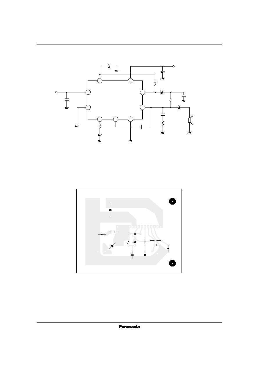
18W Audio Power Amplifier Circuit
Unit : mm
3.6
±
0.2
15.0
±
0.3
5.85
±
0.25
4.7
±
0.6
2.7
±
0.4
1.0
±
0.2
30.0
±
0.3
24.0
±
0.3
1.26
±
0.25
1.8R
5.5
±
0.3
7.5
±
0.3
11
10
9
8
7
6
5
4
3
2
1
2.54
0.7
±
0.1
3.5
±
0.25
0.35
±
0.25
0.35
+ 0.1
≠ 0.05
0.95
±
0.25
11-Lead SIP Package (HSIP011-P-0000)
9
11
6
3
5
7
8
4
1
GND (Output)
GND
(Input)
V
CC
Input
Circuit
Driver
Circuit
Output
Circuit
Ripple
Filter
Temperature
Compensation
Surge
Over Current
Protection
s
Block Diagram
AN7170
ICs for Audio Common Use
V
CC
V
CC
V
CC (surge)
I
CC
P
D
T
opr
T
stg
Supply Voltage (at no signal)
Supply Voltage (at operation)
Peak Supply Voltage
Note 1)
Supply Current
Power Dissipation
Note 2)
Operating Ambient Temperature
Storage Temperature
V
V
V
A
W
∞C
∞C
Parameter
Symbol
Rating
Unit
35
30
60
4
31.25
≠ 30 ~ + 75
≠ 55 ~ + 150
Note 1) Pulse Voltage application t = 0.2s
Note 2) Ta = 25∞C (
j ≠ c
= 4∞C/W)
s
Absolute Maximum Ratings
(Ta= 25∞C)
s
Electrical Characteristics
(V
CC
= 26.4V, f = 1kHz, Ta= 25∞C)
V
i
= 0mV
V
i
= 3mV
THD= 1%
THD= 10%
V
i
= 3mV
Parameter
Symbol
Condition
min.
typ.
max.
Unit
Quiescent Circuit Current
Voltage Gain
I
CQ
G
V
40
51
8
10.5
75
53
9.5
12
0.1
0.7
160
55
0.7
1.5
mA
dB
W
W
%
mV
Total Harmonic Distortion
No Distortion Maximum Output
Output Noise Voltage
THD
V
no
P
O
P
O
RR
Z
i
dB
k
W
W
R
g
= 10k
, DIN A Filter
V
i
= 0mV, R
g
= 0
THD= 1%
THD= 10%
Ripple Rejection Ratio
Input Impedance
No Distortion Maximum Output
40
30
13
18
(R
L
= 8
)
(R
L
= 4
)
s
Pin Descriptions
Pin No.
Pin Name
1
2
3
4
5
6
Output
NC
GND (Output)
Bootstrap
Phase Compensation
Negative Feedback
Pin No.
Pin Name
7
8
9
10
11
Input
GND (Input)
Ripple Filter
NC
V
CC
ICs for Audio Common Use
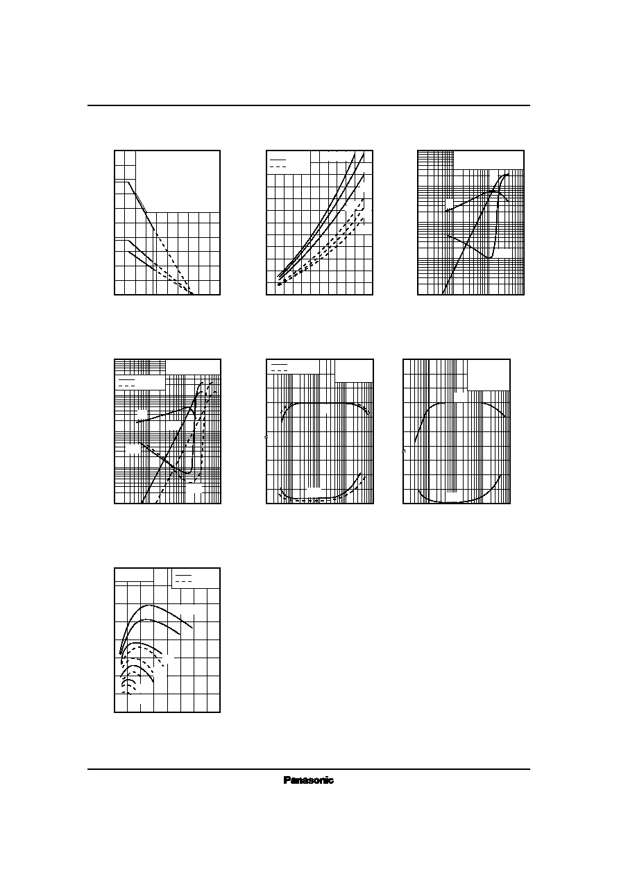
AN7170
V
CC
= 24V, R
L
= 4
f
= 1kHz, G
V
= 53dB
P
O
, P
D
, THD
≠ V
i
G
V
, THD
≠ f
G
V
, THD
≠ f
100
30
10
3
1
0.3
0.1
0.03
0.01
O
u
t
p
u
t
P
o
w
e
r
P
O
(
W
)
,
P
o
w
e
r
D
i
s
s
i
p
a
t
i
o
n
P
D
(
W
)
,
T
o
t
a
l
H
a
r
m
o
n
i
c
D
i
s
t
o
r
t
i
o
n
T
H
D
(
%
)
Input Voltage V
i
(mV)
0.1
0.3
1
3
10
30
100
V
CC
= 24V, R
L
= 8
f
= 1kHz
P
O
, P
D
, THD
≠ V
i
100
30
10
3
1
0.3
0.1
0.03
0.01
100
30
10
3
1
0.3
0.1
0.03
0.01
O
u
t
p
u
t
P
o
w
e
r
P
O
(
W
)
,
P
o
w
e
r
D
i
s
s
i
p
a
t
i
o
n
P
D
(
W
)
Input Voltage V
i
(mV)
0.1
0.3
1
3
10
30
100
V
CC
= 24V
R
L
= 8
P
O
= 2W
4
2
0
≠2
≠ 4
1.5
1.0
0.5
0
T
o
t
a
l
H
a
r
m
o
n
i
c
D
i
s
t
o
r
t
i
o
n
T
H
D
(
%
)
,
V
o
l
t
a
g
e
G
a
i
n
G
V
(
d
B
)
T
o
t
a
l
H
a
r
m
o
n
i
c
D
i
s
t
o
r
t
i
o
n
T
H
D
(
%
)
10
100
1k
10k
100k
V
CC
= 24V
R
L
= 4
P
O
= 4W
G
V
= 53dB
0
≠2
≠ 4
≠ 6
V
o
l
t
a
g
e
G
a
i
n
G
V
(
d
B
)
Frequency f (Hz)
Frequency f (Hz)
10
100
1k
10k
100k
P
D
≠ Ta
40
32
24
16
8
0
P
o
w
e
r
D
i
s
s
i
p
a
t
i
o
n
P
D
(
W
)
Ambient Temperature Ta (∞C)
0
40
80
120
160
200
P
O
≠ V
CC
24
20
16
12
8
4
0
O
u
t
p
u
t
P
o
w
e
r
P
O
(
W
)
Supply Voltage V
CC
(V)
0
12
16
20
24
28
32
R
L
= 4
R
L
= 8
P
D
≠ P
O
16
14
12
10
8
6
4
2
0
P
o
w
e
r
D
i
s
s
i
p
a
t
i
o
n
P
D
(
W
)
Output Voltage P
O
(W)
0
4
20
24
28
8
12
16
32
(1)
(2)
(3)
(1) Tc
= Ta (
j ≠ c
= 4∞C/W)
(2) With a 100cm
2
◊
3mm Al
heat sink (black color coated)
or a 200cm
2
◊
2mm Al heat
sink (not lacquered)
(3) With a 100cm
2
◊
2mm Al
heat sink (not lacquered)
2.0
1.5
1.0
0.5
0
T
o
t
a
l
H
a
r
m
o
n
i
c
D
i
s
t
o
r
t
i
o
n
T
H
D
(
%
)
G
V
= 53dB
G
V
= 46dB
G
V
= 53dB
G
V
= 46dB
R
L
= 4
R
L
= 8
28V
16V
22V
24V
10
%
G
V
G
V
THD
THD
P
O
P
O
P
D
THD
5%
THD
= 10%
1%
5%
1%
P
D
P
O
THD
V
CC
= 30V
30V
28V
16V
22V
24V
THD
f
= 1kHz