 | –≠–ª–µ–∫—Ç—Ä–æ–Ω–Ω—ã–π –∫–æ–º–ø–æ–Ω–µ–Ω—Ç: AN7171K | –°–∫–∞—á–∞—Ç—å:  PDF PDF  ZIP ZIP |
ICs for Audio Common Use
s
Overview
The AN7171NK and AN7176K are ICs for power ampli-
fication of 14W (13.2V, 4
) output. It can provide stereo
operation since two BTL amplifiers are incorporated in a
chip. It incorporates various protective circuits, thus pro-
viding high reliability. The circuits can be turned on or off
with supply pins energized, because the stand-by circuit
is built-in.
s
Features
∑
Two BTL 14W outputs built-in
∑
Stand-by circuit built-in
∑
Various protective circuits (for temperature, or against
over-voltage, short-circuit between output and earth
and between output and V
CC
, load short-circuit)
∑
Small shock noise at power ON/OFF
∑
Fewer external components required
∑
Good oscillation stability
AN7171NK, AN7176K
Dual BTL 14W Audio Power Amplifier Circuits
Unit : mm
6.33
±
0.5
29.6
±
0.3
5.9
±
0.25 7.7
±
0.3
7.8
±
0.5
1
16
29.96
±
0.3
0.6
±
0.2
1.778
¯ 3.6
28.0
±
0.3
20.0
±
0.25
R1.8
0.6
1.2
±
0.1
3.5
±
0.3
2.66
2.8
±
0.3
12.5
±
0.3
(14.1)
(4.06)
2.54
±
0.8
(0.25)
1.45
±
0.25
1.8
±
0.25
(1.2)
1.45
±
0.25
Fin-attached 16-lead ZIP package (EZIP016-P-0660)
s
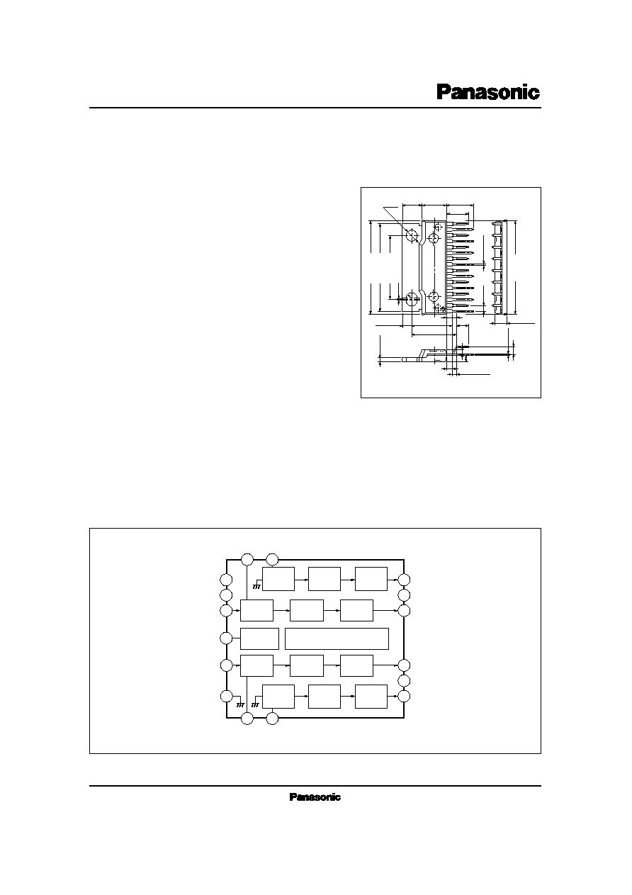
Block Diagram
1
13
6
5
12
10
11
9
14
15
16
4
3
2
8
7
V
CC
Ripple Filter
(Ch.1) IN
STAND-BY
(Ch.2) IN
GND
OUT (Ch.1) (+)
GND
OUT (Ch.1) (≠)
OUT (Ch.2) (+)
OUT (Ch.2) (≠)
GND
Input
Circuit
Driver
Circuit
Output
Circuit
Input
Circuit
Driver
Circuit
Output
Circuit
Input
Circuit
Driver
Circuit
Output
Circuit
Input
Circuit
Driver
Circuit
Output
Circuit
Stand-by
Circuit
Protection Circuit
NF
(Ch.2)
NF
(Ch.2)
NF (Ch.1)
NF (Ch.1)

ICs for Audio Common Use
AN7171NK, AN7176K
Pin No.
Pin Name
1
2
3
4
5
6
7
8
V
CC
Output Ch.1 (+)
GND (Output Ch.1)
Output Ch.1 (≠)
Stand-by
Input Ch.1
Negative Feedback Ch.1
Negative Feedback Ch.1
Pin No.
Pin Name
9
10
11
12
13
14
15
16
Negative Feedback Ch.2
GND (Input)
Negative Feedback Ch.2
Input Ch.2
Ripple Filter
Output Ch.2 (≠)
GND (Output Ch.2)
Output Ch.2 (+)
s
Pin Descriptions
s
Absolute Maximum Ratings
(Ta= 25∞C)
V
CC
Note 1)
V
CC (surge)
Note 2)
I
CC
P
D
Note 3)
T
opr
T
stg
Supply Voltage
Peak Supply Voltage
Supply Current
Power Dissipation
Operating Ambient Temperature
Storage Temperature
V
V
A
W
∞C
∞C
Parameter
Symbol
Rating
Unit
24
50.0
6.0
37.5
Note 4)
≠ 30 ~ + 75
≠ 55 ~ + 150
Note 1) When no signals
Note 2) Time = 0.2s
Note 3) R
j ≠ c
= 2∞C/W
Note 4) Ta = 75∞C
s
Electrical Characteristics
(V
CC
= 13.2V, R
L
= 4
, f = 1kHz, Ta = 25∞C)
Parameter
Symbol
Condition
min.
typ.
max.
Unit
Quiescent Current
Output Noise Voltage
Note)
Voltage Gain
Total Harmonic Distortion
Max. Output Power (4
)
mA
mVrms
dB
%
W
V
in
= 0mV
V
in
= 0mV, R
g
= 10k
V
in
= 5mV
V
in
= 5mV
THD= 10%
I
CQ
V
no
G
V
THD
P
O
Output Offset Voltage
Channel Balance
Total Harmonic Distortion
Total Harmonic Distortion
Frequency Characteristics
Frequency Characteristics
Crosstalk
Ripple Rejection Ratio
Note)
V
in
= 5mV
V
in
= 5mV, 100Hz
V
in
= 5mV, 10kHz
V
in
= 5mV, ≠3dB down
V
in
= 5mV, ≠3dB down
RR
R
g
= 0
R
g
= 0
, V
in
= 0mV,
Ripple= 300mVrms, 120Hz
V
O (offset)
CB
THD
THD
f
CH
f
CL
I
STB
CT
Stand-by Pin ON
AN7171NK
AN7176K
V
in
= 5mV, R
g
= 10k
50.5
9.0
120
0.60
52.5
0.20
12.5
200
1.50
54.5
0.75
35
40
≠200
≠1
0
0
0.26
0.45
22
21
21
650
61
400
+ 200
+ 1
1000
dB
mV
dB
%
%
kHz
Hz
µ
A
µ
A
dB
Note) With 15Hz to 30kHz (12dB/OCT) filter
Stand-by Current
Parameter
Symbol
Range
s
Recommended Operating Range
(Ta = 25∞C)
Operating Supply Voltage Range
V
CC
8.0V ~ 18.0V

ICs for Audio Common Use
AN7171NK, AN7176K
f
= 1kHz
THD
= 10%
R
L
= 4
P
O
≠ V
CC
Supply Voltage V
CC
(V)
8
12
16
20
0
4
8
12
16
20
4
M
a
x
.
O
u
t
p
u
t
P
O
(
W
)
V
CC
= 13.2V
R
L
= 4
f
= 1kHz
P
O
, THD
≠ V
in
Input Voltage V
in
(mV)
O
u
t
p
u
t
P
o
w
e
r
P
O
(
W
)
100
0.1
1
10
T
o
t
a
l
H
a
r
m
o
n
i
c
s
D
i
s
t
o
r
t
i
o
n
T
H
D
(
%
)
100
10
1.0
0.1
0.01
100
10
1.0
0.1
0.01
THD
P
O
G
V
, THD
≠ f
Frequency f (Hz)
V
o
l
t
a
g
e
G
a
i
n
G
V
(
d
B
)
100k
10
1k
10k
1.0
0.8
0.6
0.4
0.2
0
100
T
o
t
a
l
H
a
r
m
o
n
i
c
s
D
i
s
t
o
r
t
i
o
n
T
H
D
(
%
)
V
CC
= 13.2V
R
L
= 4
P
O
= 1W
f
= 1kHz
R
L
= 4
V
in
= 3mV
G
V
, THD
≠ V
CC
Supply Voltage V
CC
(V)
7
9
11
44
46
48
50
52
0
1
3
5
10
4
V
o
l
t
a
g
e
G
a
i
n
G
V
(
d
B
)
42
40
36
38
9
8
7
6
4
2
3
5
6
8
10
T
o
t
a
l
H
a
r
m
o
n
i
c
s
D
i
s
t
o
r
t
i
o
n
T
H
D
(
%
)
I
CQ
≠ V
CC
Supply Voltage V
CC
(V)
8
12
16
20
0
40
80
120
160
200
4
Q
u
i
e
s
c
e
n
t
C
u
r
r
e
n
t
I
C
Q
(
m
A
)
G
V
54
52
50
48
46
THD
G
V
THD
s
Precautions on use
1. Always attach an outside heat sink to use the chip. In addition, the outside heat sink must be fastened onto a chassis for use.
2. Connect the radiation fin to the GND potential.
3. Prevent atmospheric and ground faults, and load short-circuit.
4. The temperature protective circuit gets actuated when Tj = approx. 150∞C, but it is automatically reset when the chip
temperature drops below the above set level.
5. The overvoltage protective circuit starts the protective operation at V
CC
26V.
6. The ground fault protective circuit starts the protective operation at 0.3
or less of contact resistance.
7. The load short-circuit protective circuit starts the protective operation at 0.3
or less of contact resistance.
8. The atmospheric fault protective circuit protects the chip only from short-circuit between pins.
9. Take into consideration the heat radiation design particularly when V
CC
is set high or when the load is 2
.

ICs for Audio Common Use
ICs for Audio Common Use
IN 2
OUT 2≠2
0.1
µ
F
2.2
0.1
µ
F
IN 1
OUT 1≠2
0.1
µ
F
2.2
OUT 1≠1
2.2
AN7171NK, AN7176K
2.2
1
µ
F
200
200
0.047
µ
F
0.047
µ
F
200
µ
F
100
µ
F
100
µ
F
1
µ
F
2000
µ
F
GND
0.1
µ
F
MUTE
OUT 2≠1
+
+
≠
≠
+
≠
+
≠
5
11
9
12
7
8
6
10
1
4
3
2
14
15
16
13
≠
+
≠
+
≠
+
≠
+
≠
+
≠
+
AN7171NK
AN7176K
GND
GND
(STAND-BY)
OUT Ch.2
4
OUT Ch.1
4
2000
µ
F
0.1
µ
F
0.1
µ
F
2.2
2.2
0.1
µ
F
0.1
µ
F
2.2
2.2
200
µ
F
Ripple Filter Pin
V
CC
=13.2V
V
CC
Pin
IN Ch.1
1
µ
F
100
µ
F
200
IN Ch.2
1
µ
F
100
µ
F
200
0.047
µ
F
0.047
µ
F
GND (Input side)
0V
+5V (Stand-by mode)
+5V
0V (Stand-by mode)
AN7171NK :
AN7176K :
s
Application Circuit
s
Printed Circuit Board Layout