 | –≠–ª–µ–∫—Ç—Ä–æ–Ω–Ω—ã–π –∫–æ–º–ø–æ–Ω–µ–Ω—Ç: AN7190NK | –°–∫–∞—á–∞—Ç—å:  PDF PDF  ZIP ZIP |

ICs for Audio Common Use
1
AN7190NK, AN7190NZ
Dual 20 W BTL power amplifier
s
Overview
The AN7190NK and the AN7190NZ are audio power
ICs developed for the sound output of car audio (dual 20
W). It is incorporating various protective circuits to pro-
tect the IC from destruction by GND-open, short circuit
to GND and power supply surge which are the important
subject of power IC protection, so the IC will largely
contribute to a high reliability design of equipment. Also,
it is incorporating a perfect muting circuit which is free
from shock noise, so that a shock noise design under the
set transient condition can be made easily using together
with its standby function.
s
Features
∑
BTL 20 W
◊
2-channel (4
), G
V
=
40 dB
∑
Built-in various protection circuits (thermal protection,
short circuit to V
CC
and short circuit to GND, V
CC
-open
short circuit to V
CC
, GND-open short circuit to GND,
overvoltage and supply surge, and ASO, etc.)
Especially, the supply surge breakdown voltage is 100
V or more.
GND open breakdown voltage is 16 V or more.
∑
Built-in standby function
Free from shock noise at STB on/off.
∑
Built-in muting function
Free from shock noise at mute-on/off.
Adapting attenuator method so that abnormal sound due
to waveform deformation is not generated .
Attack time, recovery time are 50 ms or less.
∑
Reduction in external components
It eliminates the need for NF and BS electrolytic ca-
pacitors.
Muting function is not required, and power supply choke
coil is unnecessary.
∑
Provided with beep sound input pin
∑
2
load guaranteed
s
Applications
∑
Car audio
HZIP016-P-0665A
AN7190NK
Unit : mm
HZIP015-P-0745A
AN7190NZ
Unit : mm
11.3±0.3
7.7±0.3
(10.0)
29.6±0.3
(10.0)
20.0±0.3
28.0±0.3
29.75±0.3
(0.6)
0.6
(0.889)
(1.1)
(0.889)
16
1
+0.15 -
0.10
3.6
R1.8
3.5±0.2
1.788
1.45±0.15
1.80±0.15
(2.54)
1.2+0.1
0.25
+0.10 -
0.05
(12.5)
(14.1)
(18.7)
(1.2)
(21.5)
(17.63)
R0.7
18.00±0.30
13.50±0.30
3.60±0.10
10.0±0.30
1
15
4.00±0.20
1.50±0.10
0.50
+0.20
≠0.10
(0.61)
(2.54)
0.25
+0.15
≠0.05
R0.55
3.25±0.10
13.25±0.30
18.95±0.50
15.65±0.50
1.27
(1.80)
(1.95)
19.00±0.30
19.30±0.30
2.40±0.50

AN7190NK, AN7190NZ
ICs for Audio Common Use
2
s
Pin Descriptions
s
Absolute Maximum Ratings
Parameter
Symbol
Rating
Unit
Supply voltage
*2
V
CC
25
V
Peak supply voltage
*3
V
surge
80
V
Supply current
I
CC
9.0
A
Power dissipation
*4
P
D
AN7190NK
32.5
W
AN7190NZ
59
Operating ambient temperature
*1
T
opr
-
30 to
+
85
∞
C
Storage temperature
*1
T
stg
-
55 to
+
150
∞
C
Note) *1 : T
a
=
25
∞
C except operating ambient temperature and storage temperature.
*2 : Without signal
*3 : Time
=
0.2 s
*4 : T
a
=
85
∞
C
s
Block Diagram
Pin No.
Description
1
Power supply
2
Ch.1 output (
+
)
3
Grounding (output ch.1)
4
Ch.1 output (
-
)
5
Standby
6
Ch.1 input
7
Muting
8
Grounding (sub)
Pin No.
Description
9
Grounding (input)
10
Beep sound input
11
Ch.2 input
12
Ripple filter
13
Ch.2 output (
-
)
14
Grounding (output ch.2)
15
Ch.2 output (
+
)
Ref.
Protection cct.
Att.con.
Att.
Att.
Att.
Att.
3
4
2
14
13
12
1
V
CC
8
GND (sub)
GND (input)
Beep in
Ch.1 in
Ch.2 in
Standby
Mute
10
6
5
7
11
9
15
Ch.1 GND
Ch.2 GND
Ch.1 out (
-
)
Ch.1 out (
+
)
Ch.2 out (
-
)
Ch.2 out (
+
)
ICs for Audio Common Use
AN7190NK, AN7190NZ
3
s
Electrical Characteristics at V
CC
=
13.2 V, freq.
=
1 kHz, T
a
=
25
∞
C
Parameter
Symbol
Conditions
Min
Typ
Max
Unit
Quiescent current
I
CQ
V
IN
=
0 mV, R
L
=
4
120
250
mA
Standby current
I
STB
V
IN
=
0 mV, R
L
=
4
1
10
µ
A
Output noise voltage
*1
V
NO
R
g
=
4.7 k
, R
L
=
4
0.22
0.5
mV[rms]
Voltage gain 1
G
V1
V
IN
=
20 mV, R
L
=
4
38
40
42
dB
Total harmonic distortion 1
THD
1
V
IN
=
20 mV, R
L
=
4
0.07
0.4
%
Maximum output power 1
P
O1
THD
=
10
%
, R
L
=
4
16
18
W
Ripple rejection ratio
*1
RR
R
L
=
4
, R
g
=
4.7 k
, V
r
=
1 V[rms],
60
72
dB
f
r
=
1 kHz
Channel balance
CB
V
IN
=
20 mV, R
L
=
4
0
1
dB
Cross-talk
*1
CT
V
IN
=
20 mV, R
L
=
4
, R
g
=
4.7 k
55
65
dB
Output offset voltage
V
OFF
R
g
=
4.7 k
, R
L
=
4
-35
0
0
350
mV
Muting effect
*1
MT
V
IN
=
20 mV, R
L
=
4
70
82
dB
Input impedance
Z
I
V
IN
= ±
0.3 V
DC
22
28
35
k
Voltage gain 2
G
V2
V
IN
=
20 mV, R
L
=
2
38
40
42
dB
Total harmonic distortion 2
THD
2
V
IN
=
20 mV, R
L
=
2
0.1
0.5
%
Maximum output power 2
P
O2
THD
=
10
%
, R
L
=
2
16
24
W
Shock noise
*2
V
S
R
L
=
4
, R
g
=
4.7 k
, V
MUTE
=
5 V,
-
100
0
100
mV[p-0]
V
STB
=
on/off,
50 Hz HPF on
Total harmonics distortion 3
THD
3
V
IN
=
5 mV, f
IN
=
20 kHz
0.10
0.5
%
R
g
=
4.7 k
, R
L
=
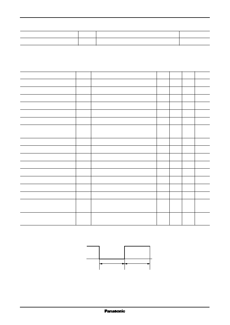
Note) *1 : Measurement using a bandwidth 15 Hz to 30 kHz (12 dB/OCT) filter.
*2 : For V
STB
=
on/off, change over the standby terminal by the voltages of 0 V and 5 V at the time shown below.
Standby terminal voltage
s
Recommended Operating Range
Parameter
Symbol
Range
Unit
Supply voltage
V
CC
8.0 to 18.0
V
5 V
0 V
120 ms
120 ms

AN7190NK, AN7190NZ
ICs for Audio Common Use
4
s
Usage Notes
1. Always attach an outside heat sink when using the chip. Note that, the outside heat sink must be fastened onto a
chassis for use.
2. Connect the cooling fin to GND potential.
3. Avoid short circuit to V
CC
and short circuit to GND, and load short-circuit.
4. The temperature protection circuit will be actuated at T
j
=
approx. 150
∞
C, but it is automatically reset when the chip
temperature drops below the above set level.
5. The overvoltage protection circuit starts its operation at V
CC
=
approx. 20 V.
6. Take into consideration the heat radiation design particularly when V
CC
is set high or when the load is 2
.
7. When the beep sound function is not used, open the beep sound input pin (pin 10) or connect it to pin 9 with around
0.01
µ
F capacitor.
8. Connect only pin 9 (ground, signal source) to the signal GND of the amplifier in the previous stage. The character-
istics such as distortion, etc. will improve.
0
20
40
60
80
100
120
113.6
40.3
59.5
30.5
20.5
11.3
1.8
0
25
50
75
100
125
150
Ambient temperature T
a
(∞
C)
Po
wer dissipation P
D
(W)
Infinite heat sink
1
∞
C/W heat sink
2
∞
C/W heat sink
3
∞
C/W heat sink
5
∞
C/W heat sink
10
∞
C/W heat sink
Without heat sink
R
th (j
-
c)
=
1.1
∞
C/W
R
th (j
-
a)
=
68.3
∞
C/W
s
Technical Information
∑
P
D
T
a
curves of packages
∑ HZIP016-P-0665A (AN7190NK)
∑ HZIP015-P-0745A (AN7190NZ)
P
D
T
a
P
D
T
a
0
10
20
17.9
35
41.7
45
40
55
50
60
65
62.5
25
31.3
30
15
10.4
5
3.0
0
25
50
75
100
125
150
Ambient temperature T
a
(∞
C)
Po
wer dissipation P
D
(W)
Infinite heat sink
1
∞
C/W heat sink
2
∞
C/W heat sink
3
∞
C/W heat sink
5
∞
C/W heat sink
10
∞
C/W heat sink
Without heat sink
R
th (j
-
c)
=
2
∞
C/W
R
th (j
-
a)
=
42
∞
C/W

ICs for Audio Common Use
AN7190NK, AN7190NZ
5
s
Application Circuit Example
1
2 200
µ
F
0.22
µ
F
2.2
2.2
4.7 k
4.7 k
10
µ
F
0.22
µ
F
2
3
4
5
6
V
IN
(ch.1)
Beep in
V
IN
(ch.2)
C
RF
V
CC
7
8
9
10
11
12
13
14
15
33
µ
F
4.7 k
1
µ
F
5 V
0 V
STB
5 V
0 V
Mute
2/4
0.22
µ
F
2.2
2.2
0.22
µ
F
2/4
Note) Standby state when STB pin is open-circuit.
Mute off when mute terminal is open-circuit.
Replace the C
RF
with 10
µ
F capacitor when shock noise (V
S
) is measured.