 | –≠–ª–µ–∫—Ç—Ä–æ–Ω–Ω—ã–π –∫–æ–º–ø–æ–Ω–µ–Ω—Ç: AN7194K | –°–∫–∞—á–∞—Ç—å:  PDF PDF  ZIP ZIP |
ICs for Audio Common Use
1
AN7194K, AN7194Z
Dual BTL 50 W single power supply class-H power amplifier IC
s
Overview
The AN7194K and AN7194Z are single power sup-
ply, BTL, audio class-H power amplifier ICs. A class-H
power amplifier can be made up when this ICs are used in
combination with the AN7077Z which is separately mar-
ket-available, and it is possible to make a low consump-
tion power system. Also, the AN7194K and AN7194Z
are incorporating various protection circuits, so that those
ICs contribute to the high reliability design of set.
s
Features
∑
Incorporating various protection circuits :
Thermal protection, load short-cirucit, short circuit to
V
CC
and short circuit to GND, overvoltage.
∑
Built-in stand-by function
(Free from shock noise when standby turns-on/off)
∑
Built-in muting function
Free from shock noise at mute-on/off
Adapting attenuator method so that abnormal sound is
not generated due to waveform deformation
Attack time, recovery time are 20 ms or less
∑
Reduction in external components
NF and BS electrolytic capacitors are needless
RF electrolytic capacitor is needless
External muting function is needless
∑
OR output terminal is provided
∑
Designed for headphone use
∑
The AN7194K is of a 16-pin and the AN7194Z is of a
15-pin package
s
Applications
∑
Miniature audio component, CD player radio cassette,
karaoke are other audio equipment
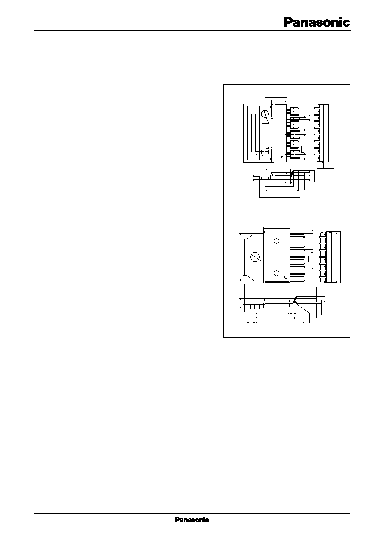
HZIP016-P-0665B
11.3±0.3
7.7±0.3
(10.0)
29.6±0.3
(10.0)
20.0±0.3
28.0±0.3
29.75±0.3
(0.6)
0.6
(0.889)
(1.1)
(0.889)
16
1
+0.15 -
0.10
3.6
R1.8
3.5±0.2
1.788
1.45±0.15
1.80±0.15
(2.54)
1.2+0.1
0.25
+0.10 -
0.05
(12.5)
(14.1)
(18.7)
(1.2)
(21.5)
(17.63)
R0.7
AN7194K
HZIP015-P-0745A
AN7194Z
18.00±0.30
13.50±0.30
3.60±0.10
10.0±0.30
11
5
4.00±0.20
1.50±0.10
0.50
+0.20
≠0.10
(0.61)
(2.54)
0.25
+
0.15
≠0.05
R0.55
3.25±0.10
13.25±0.30
18.95±0.50
15.65±0.50
1.27
(1.80)
(1.95)
19.00±0.30
19.30±0.30
2.40±0.50
AN7194K, AN7194Z
ICs for Audio Common Use
2
s
Pin Descriptions
s
Absolute Maximum Ratings
Parameter
Symbol
Rating
Unit
Supply voltage
V
CC
26
V
Supply current
I
CC
9.0
A
Power dissipation
*2
P
D
AN7194K
37.5
W
AN7194Z
68.2
Operating ambient temperature
*1
T
opr
-
25 to
+
75
∞
C
Storage temperature
*1
T
stg
-
55 to
+
150
∞
C
Note) *1 : All items are at T
a
=
25
∞
C, except for the operating ambient temperature and storage temperature.
*2 : The value when R
th(j-c)
=
1.1
∞
C/W, and T
a
=
75
∞
C
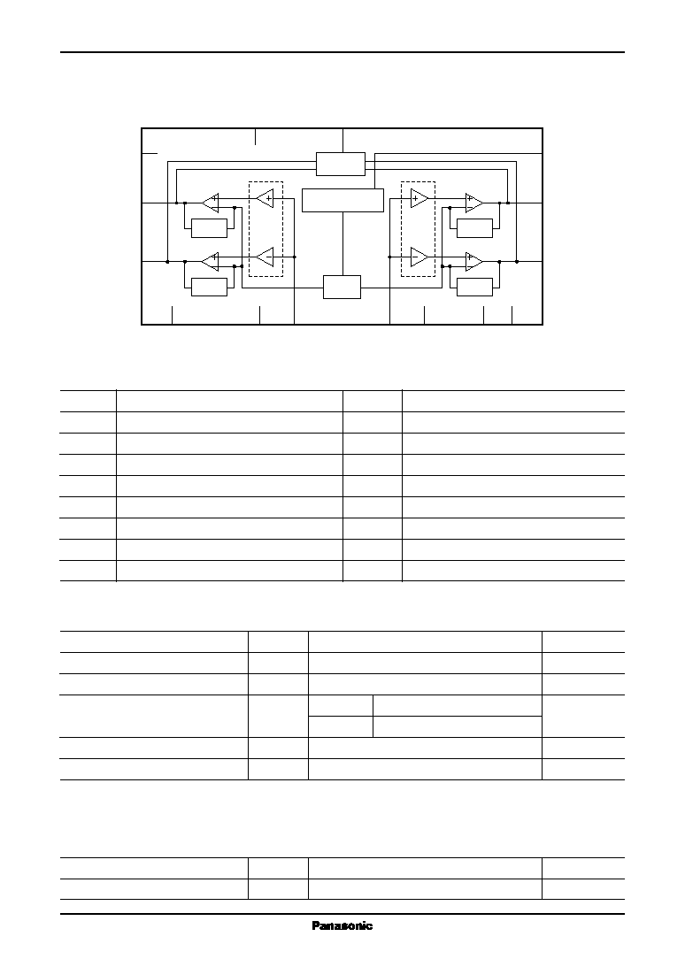
Pin No.
Description
1
Power supply
2
Ch.1 output (
-
)
3
Grounding (output ch.1)
4
Ch.1 output (
+
)
5
Stand-by
6
Ch.1 input
7
Muting
8
Middle point (1/2 V
CC
)
Pin No.
Description
9
OR output
10
GND
11
Ch.2 input
12
N.C.
13
Ch.2 output (
+
)
14
Grounding (output ch.2)
15
Ch.2 output (
-
)
16
N.C. (for the AN7194K only)
s
Recommended Operating Range
Parameter
Symbol
Range
Unit
Supply voltage
V
CC
6.0 to 24.0
V
s
Block Diagram
OR
Ripple filter
1/2
34 dB
12
2
4
1
15
9
8
1/2 V
CC
GND
14
6
5
GND
10
7
11
13
V
CC
34 dB
34 dB
34 dB
3

ICs for Audio Common Use
AN7194K, AN7194Z
3
s
Electrical Characteristics at V
CC
=
12 V, f
=
1 kHz, T
a
=
25
∞
C
Note) *1 : Measurement using a bandwidth 15 Hz to 30 kHz (12 dB/OCT) filter.
*2 : V
CC
=
24 V
Parameter
Symbol
Conditions
Min
Typ
Max
Unit
Quiescent current
I
CQ
V
IN
=
0 mV, R
L
=
6
150
250
mA
Standby current
I
STB
V
IN
=
0 mV, R
L
=
6
1
10
µ
A
Output noise voltage
*1
V
NO
R
G
=
10 k
, R
L
=
6
0.22
0.5
mV[rms]
Voltage gain
G
V
V
IN
=
24.5 mV, R
L
=
6
38
40
42
dB
Total harmonics distortion
THD
V
IN
=
24.5 mV, R
L
=
6
0.2
0.6
%
Maximum output power 1
P
O1
THD
=
10%, R
L
=
6
8
10
W
Maximum output power 2
*2
P
O2
THD
=
10%, R
L
=
6
30
44
W
Ripple rejection ratio
*1
RR
R
L
=
6
, R
G
=
10 k
45
60
dB
V
R
=
1 V[rms], f
R
=
1 kHz
Channel balance
*1
CB
V
IN
=
24.5 mV, R
L
=
6
-
1
0
1
dB
Cross-talk
*1
CT
V
IN
=
24.5 mV, R
L
=
6
, R
G
=
10 k
50
60
dB
Output offset voltage
V
OFF
R
G
=
10 k
, R
L
=
6
-
300
0
300
mV
Muting effect
*1
MT
V
IN
=
24.5 mV, R
L
=
6
60
82
dB
Standby terminal voltage
I
CQ-STB
V
IN
=
open, V
STB
=
5 V
50
µ
A
s
Usage Notes
1. Always attach an outside heat sink when using the chip. In addition, the outside heat sink must be fastened onto
a chassis for use.
2. Connect the cooling fin to GND potential.
3. Avoid short circuit to V
CC
and short circuit to GND, and load short-circuit.
4. The temperature protection circuit will be actuated at T
j
=
approx. 150∞C.
However, it is automatically reset when the chip temperature drops below the above set level.
5. The overvoltage protection circuit starts its operation at V
CC
=
approx. 26 V.
6. For the standby voltage, a stabilized power supply of 3 V or higher should be used.
7. Only when being used in combination with the AN7077Z, this IC can operate up to the supply voltage of approx.
25.4 V which is the maximum output voltage of the AN7077Z.

AN7194K, AN7194Z
ICs for Audio Common Use
4
s
Application Circuit Example
s
Technical Information
∑
P
D
T
a
curves of packages
Note) After fixing all of the lead wires to printed circuit board by soldering, use the IC after fixing the printed circuit board and
the cooling fin of the IC.
∑ AN7194K (HZIP016-P-0665B)
∑ AN7194Z (HZIP015-P-0745A)
P
D
T
a
P
D
T
a
R
th (j
-
c)
=
2
∞
C/W
R
th (j
-
a)
=
48
∞
C/W
85
62.5
5
10
15
20
25
30
35
31.3
40
45
50
5
60
65
70
75
80
41.7
17.9
10.4
2.6
0
0
25
50
75
100
125
150
Infinity heat sink
1
∞
C/W
heat sink
2
∞
C/W
heat sink
3
∞
C/W
heat sink
5
∞
C/W
heat sink
10
∞
C/W
heat sink
Without heat sink
Ambient temperature T
a
(∞
C)
Po
wer dissipation P
D
(W)
85
68.2
5
10
15
20
25
30
35
31.5
40
45
50
5
60
65
70
75
80
41.0
21.7
12.7
0
0
25
50
75
100
125
150
Infinity heat sink
2
∞
C/W heat sink
3
∞
C/W heat sink
5
∞
C/W heat sink
10
∞
C/W heat sink
R
th (j
-
c)
=
1.1
∞
C/W
R
th (j
-
a)
=
68.3
∞
C/W
1
∞
C/W heat sink
Ambient temperature T
a
(∞
C)
Po
wer dissipation P
D
(W)
12
2
4
2.2
0.22
µ
F
5 V
±
0.5 V
V
TH
=
3.5 V
5 V
±
0.5 V
V
TH
=
2.8 V
1
15
9
8
150 k
STB
V
IN1
V
IN2
Mute
10 k
10 k
14
6
5
10
7
11
13
3
2.2
0.22
µ
F
2.2
0.22
µ
F
47
µ
F
2.2
0.22
µ
F
4.7 k
10
µ
F
10
µ
F