s
Overview
The AN7367K is an integrated circuit available for
stereo operation on a single chip developed for dbx
II
type noise reduction, which can also use for U.S. sound
multiplex TV. And it is designed for easy use of reference
signal level, supply voltage and logic input level.
s
Features
∑
Dynamic range : 110dB
∑
2-channel
∑
Reference input-output signal level : 90mV
∑
2 power supply type (+, ≠)
ICs for Cassette, Cassette Deck
AN7367K
dbx
II
Noise Reduction IC for Cassette Deck
1
2
3
4
5
6
7
8
9
10
11
12
13
14
19
18
17
16
15
20
21
22
23
24
25
26
27
28
26.7
±
0.3
8.4
±
0.3
3 ~ 15∞
0.3
+ 0.1
≠ 0.05
4.8
±
0.25
1.05
±
0.25
3.05
±
0.25
1.778
0.5
±
0.1
0.9
±
0.25
Unit : mm
10.16
±
0.25
28-Lead SDIP Package (SDIP028-P-0400A)
28
27
26
25
24
23
22
21
20
19
18
17
16
15
1
2
3
4
5
6
7
8
9
10
11
12
13
14
+
≠
A
+
≠
C
+
≠
E
+
≠
B
+
≠
D
+
≠
F
B D E
E O D E O D
E O D
E O D
L.S
+V
CC
≠V
CC
GND
s
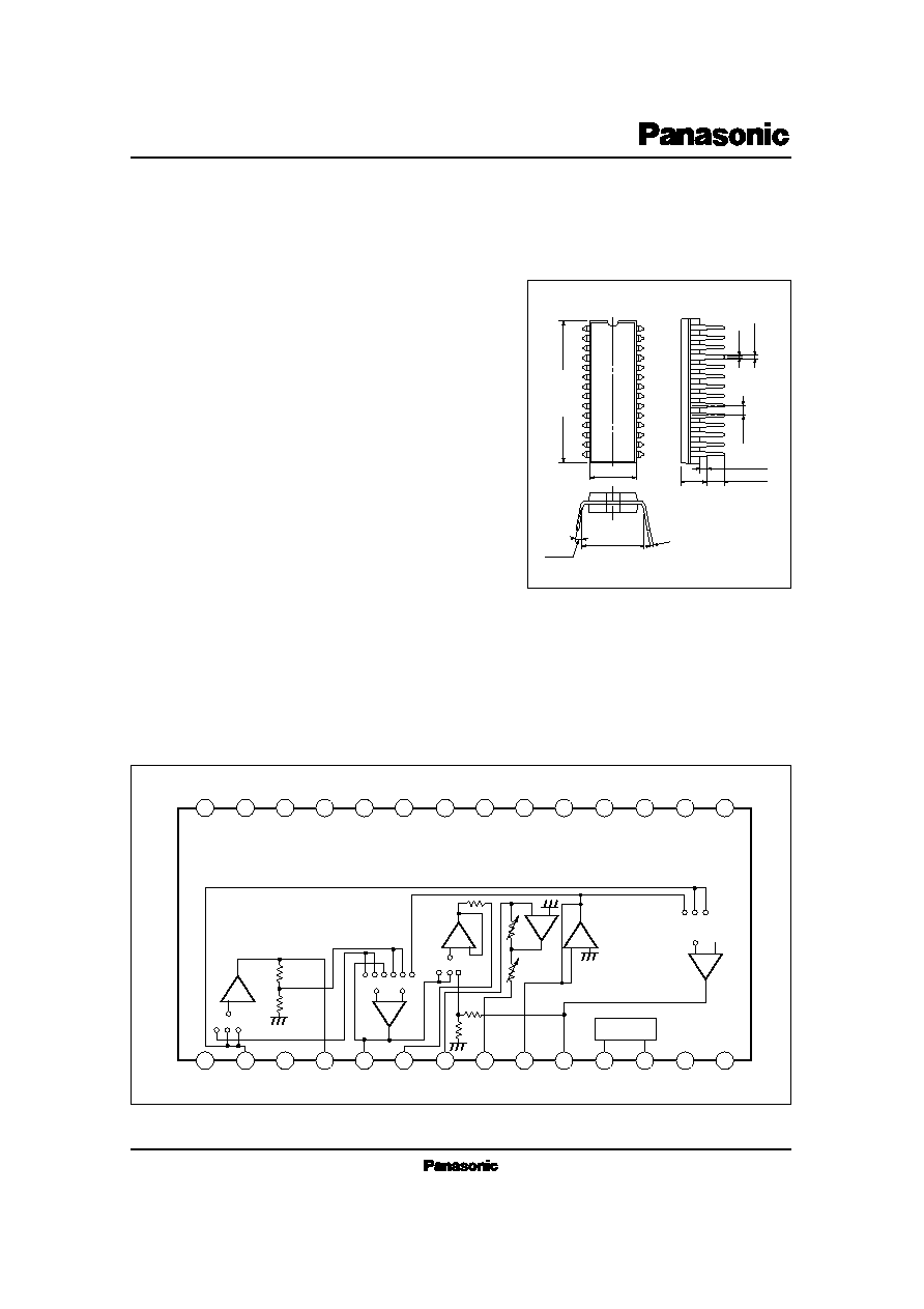
Block Diagram

ICs for Cassette, Cassette Deck
AN7367K
s
Absolute Maximum Ratings
(Ta=25∞C)
V
CC
I
CC
P
D
T
opr
T
stg
Supply Voltage
Supply Current
Power Dissipation (Ta=75∞C)
Operating Ambient Temperature
Storage Temperature
V
mA
mW
∞C
∞C
Parameter
Symbol
Rating
Unit
±
7.2
30
450
≠20 ~ + 75
≠55 ~ + 150
s
Recommended Operating Range
(Ta=25∞C)
±
5V ~
±
7V
Parameter
Symbol
Range
Operating Supply Voltage Range
V
CC
AN7367K H4
s
Electrical Characteristics
(V
CC
=
±
6V, Ta=25∞C )
Encode Output Voltage
Encode Linearity ≠1 *
1
Encode Linearity ≠2 *
1
Decode Output Voltage
Decode Linearity ≠1 *
2
Decode Linearity ≠2 *
2
Encode Max. Output Voltage
Decode Max. Output Voltage
Encode Total Harmonic Distortion
Decode Total Harmonic Distortion
Encode Noise Output Voltage
Decode Noise Output Voltage
Encode Output Defference between Channels
Decode Output Difference between Channels
Encode Crosstalk between Channels
Decode Crosstalk between Channels
Monitor Output Voltage
Monitor Output Voltage Output Difference Between Channels
Monitor Output Noise Output Voltage
Monitor Output Total Harmonic Distortion
dbx OFF Line Output Voltage
dbx OFF Rec. Output Voltage
dbx OFF line Output Total Harmonic Distortion
dbx OFF Rec Output Total Harmonic Distortion
dbx OFF Line Output Noise Output Voltage
dbx OFF Rec. Output Noise Output Voltage
dbx OFF Line Output Output Difference between Channels
dbx OFF Rec. Output Output Difference between Channels
Input Impedance
Total Circuit Current
V
OE
L
E ≠ 1
L
E ≠ 2
V
OD
L
D ≠ 1
L
D ≠ 2
V
OME
V
OMD
THD
E
THD
D
V
NOE
V
NOD
CD
E
CD
D
CT
E
CT
D
V
OM
CD
M
V
NOM
THD
M
V
LOFF
V
ROFF
THD
LOFF
THD
ROFF
V
NLOFF
V
NROFF
CD
LOFF
CD
ROFF
Z
IN
I
tot
V
in
= 1kHz, 90mV (Reference Level)
V
in
= 1kHz, 900mV (Encode)
V
in
= 1kHz, 0.9mV (Encode)
V
in
= 1kHz, 90mV (Reference Level)
V
in
= 1kHz, 285mV (Decode)
V
in
= 1kHz, 9mV (Decode)
THD
= 3%, f
= 1kHz
THD
= 3%, f
= 1kHz
At Encode, 400Hz ~ 30kHz, f
= 1kHz, 90mV
At Decode, 400Hz ~ 30kHz, f
= 1kHz, 90mV
Input short, DIN/AUDIO
Input short, DIN/AUDIO
V
in
= 1kHz, 90mV
V
in
= 1kHz, 90mV
At Encode *
3
, V
in
= 1kHz, 900mV
At Decode, V
in
= 1kHz, 90mV
At Encode, V
in
= 1kHz, 90mV
At Encode, V
in
= 1kHz, 90mV
Encode input, Short DIN/AUDIO
At Encode, V
in
= 1kHz, 90mV
V
in
= 1kHz, 180mV
V
in
= 1kHz, 180mV
V
in
= 1kHz, 180mV
V
in
= 1kHz, 180mV
Input Short, DIN/AUDIO
Input Short, DIN/AUDIO
V
in
= 1kHz, 180mV
V
in
= 1kHz, 180mV
V
in
= 1kHz, 90mV
Input Short at Encode
67.5
8
≠ 22
67.5
17
≠ 43
300
1100
≠ 1.3
≠ 2
75
≠ 1.5
151
151
≠ 1.5
≠ 1.5
500
85
10
≠ 20
85
20
≠ 40
0.35
0.1
≠ 62
≠ 96
0
0
≠ 52
≠ 91
90
0
≠ 110
0.01
180
180
0.01
0.01
≠ 110
≠ 110
0
0
12
107
12
≠ 18
107
23
≠ 37
0.45
0.3
≠ 58
≠ 92
1.3
2
≠ 45
≠ 85
107
1.5
≠ 106
0.1
214
214
0.1
0.1
≠ 104
104
1.5
1.5
16
mV
dB
dB
mV
dB
dB
mV
mV
%
%
dBV
dBV
dB
dB
dBV
dBV
mV
dB
dBV
%
mV
mV
%
%
dBV
dBV
dB
dB
k
mA
Parameter
Symbol
Condition
min.
typ.
max.
Unit
*1 Level Ratio to V
OE
*2 Level Ratio to V
OD
*3 Measure output leak by short of measuring channel input and input to reverse channel.
ICs for Cassette, Cassette Deck
AN7367K
s
Electrical Characteristics (Cont.)
(V
CC
=
±
6V, Ta=25∞C)
dbx ON/OFF Control dbx ON
dbx ON/OFF Control dbxOFF
Encode/Decode Control Encode
Encode/Decode Control Decode
dbx ON/OFF Control "L" Overflow Current
Encode/Decode Control "L" Overflow Current
Pulse Noise at Encode
V
15ON
V
15OFF
V
16EN
V
16DE
I
15L
I
16L
V
NPE
Satisfy specifications of the preceding page V
OE
~ V
NLOFF
Satisfy specifications of the preceding page V
OE
~ V
NLOFF
V
15
=1.8V
V
16
=1.8V
Input Short, Time : a second, number : one
3.2
3.2
≠2.1
≠2.1
6
1.8
6
1.8
≠ 0.2
≠ 0.2
13
V
V
V
V
µ
A
µ
A
mV
P ≠ P
Parameter
Symbol
Condition
min.
typ.
max.
Unit
≠V
EE
+ 0.4V
≠V
EE
+ 0.4V
Satisfy specifications of the preceding page
V
OE
~ V
NLOFF
Satisfy specifications of the preceding page
V
OE
~ V
NLOFF
20
0
≠20
≠ 40
≠ 60
≠80
≠100
≠ 60
≠ 40
≠20
0
2
1
0
V
CC
=
±
6V
LPF
= 30kHz
HPF
= 400Hz
Din Audio ≠ 62dBV
Vout = 85.6mV = 0dB
f = 1kHz
V
in
= 90mV
f
1kHz ∑∑∑ LPF (30kHz)
HPF (400Hz)
f <1kHz ∑∑∑ HPF (400Hz)
V
CC
=
±
6V
LPF = 30kHz
HPF = 400Hz
Din Audio ≠ 98dBV
V
o
u
t
(
d
B
V
)
V
o
u
t
(
d
B
)
V
o
u
t
(
d
B
V
)
V
in
(dBV)
V
in
(dBV)
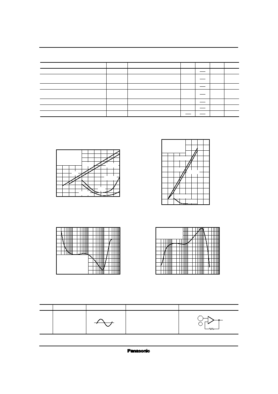
Input/Output Characteristics
(Rec. Mode)
Output Frequency Characteristics
(Rec. Mode)
Input/Output Characteristics
(Playback Mode)
≠100
≠ 80
≠ 60
≠ 40
≠ 20
0
1.6
1.2
0.8
0.4
0
≠10
≠20
≠30
≠40
≠50
≠60
T
H
D
(
%
)
T
H
D
(
%
)
10
100
1k
10k
100k
6
4
2
0
≠ 2
≠ 4
Frequency f (Hz)
Vout = 87.6mV = 0dB
f = 1kHz
V
in
= 90mV
V
o
u
t
(
d
B
)
Output Frequency Characteristics
(Playback Mode)
10
100
1k
10k
100k
8
4
0
≠ 4
≠ 8
≠ 12
Frequency f (Hz)
f=1kHz
f=10kHz
f=10kHz
THD
f=1kHz
V
out
f = 1kHz
f = 1kHz
f = 10kHz
V
out
THD
s
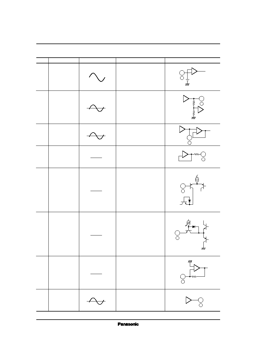
Characteristics Curve
Equivalent Circuit
Pin Name
Pin No.
Typ. Waveform
Description
2
∑
27
Pin for inputting signal
≠
+
2
27
0V
Recording Signal
Input
s
Pin Description