 | ÐлекÑÑоннÑй компоненÑ: AN7504SB | СкаÑаÑÑ:  PDF PDF  ZIP ZIP |
Äîêóìåíòàöèÿ è îïèñàíèÿ www.docs.chipfind.ru
ICs for Audio Common Use
1
Publication date: December 2001
SDC00029BEB
AN7504SB
Pre-amp. and power amp. IC for 1.5 V headphone stereo
I Overview
The AN7504SB is a low voltage operation headphone
amp. IC for headphone C-cassette stereo. It incorporates
tape selector, pre-amp. , soft AGC bass-boost circuit, etc.
I Features
· Low voltage operation (0.98 V to 2.0 V)
· Tape selector switch built-in
· Low frequency boost function with soft AGC
I Applications
· Headphone stereo
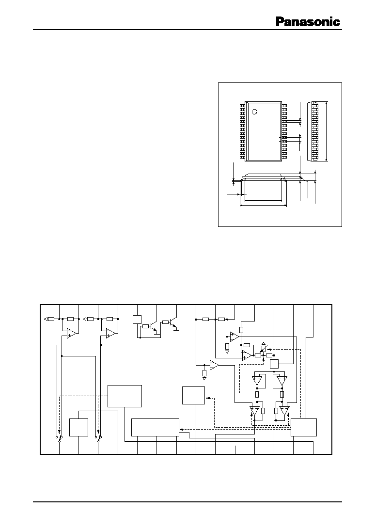
I Block Diagram
SSOP028-P-0375A
Unit: mm
0.3
±
0.1
0.1
±
0.1
(0.4)
2.05
±
0.2
0.9
±
0.1
0
.9
±
0.1
0.2
+
0.1
-
0.05
1
11.6
±
0.3
9.3
±0.3
7.2
±0.3
14
28
15
0.8
12
8
Pre-in (R)
V
REF
Pre-in (L)
Pre-out (R)
Lo
w BST
T
ape-select
Pre-out (L)
PWR-in (L)
PWR-in (R)
V
RPF
PWR-out (L)
V
CCP
PWR-out (R)
REV/FWD/
Pre-mute
STB/PWR mute
GND
2
27
3
26
4
25
5
24
6
23
7
22
8
21
9
20
10
19
11
18
12
17
13
16
14
15
Control
FWD/REV
Pre-mute
Ripple filter
Bias
AGC
Note) The package of this product will be changed
to lead-free type (SSOP028-P-0375E). See the
new package dimensions section later of this
datasheet.
AN7504SB
2
SDC00029BEB
I Absolute Maximum Ratings
Parameter
Symbol
Rating
Unit
Supply voltage
V
CC
2.1
V
Supply current
I
CC
20
mA
Power dissipation
*2
P
D
42
mW
Operating ambient temperature
*1
T
opr
-20 to +70
°C
Storage temperature
*1
T
stg
-55 to +125
°C
I Recommended Operating Range
Parameter
Symbol
Range
Unit
Supply voltage
V
CC
0.98 to typ. 1.2 to 2.0
V
I Electrical Characteristics at V
CC
= 1.2 V, f = 1 kHz, R
L
= 32 , T
a
= 25°C
Note) *1: Except for the operating ambient temperature and storage temperature, all ratings are for T
a
= 25°C.
Keep V
CC
(0.95 V to 0.98 V) free from any abnormal operation such as oscillation.
*2: The power dissipation shown is the value for T
a
= 75°C. For the independent IC without a heat sink.
Parameter
Symbol
Conditions
Min
Typ
Max
Unit
Voltage gain
G
V
V
O
= -22.2 dBV
54
57
60
dB
Circuit current 1
I
CC1
V
IN
= 0, R
G
= 2.2 k, LBST off
2.2
5.3
mA
Pre-amp. block
Closed circuit voltage gain
G
VC(PB)
V
O
= -22.2 dBV
32.5
34
35.5
dB
Max. output voltage
V
Omax(PB)
THD
= 1%, 30 kHz LPF on
120
210
mV
Total harmonic distortion
THD
(PB)
V
O
= 22.2 dBV, 30 kHz LPF on
0.2
0.6
%
G
VC
= 35 dB (NAB)
Output noise voltage
V
NO(PB)
R
G
= 2.2 k, 1HF-A
-90
-76
dBV
Mute attenuation
G
MUTE(PB)
Ratio as V
O
= -22.2 dBV
-85
-70
dB
Pre-mute on
Boost low sound and power amp. block
Voltage gain 1
G
V1(PW)
V
O
= -22.2 dBV
21
23
25
dB
Voltage gain 2
G
V2(PW)
LBOOST on, V
O
= -22.2 dBV
21.4
23.4
25.4
dB
Rating output power
P
OUT
THD
= 10%, 30 kHz LPF on
2.5
4.5
mW
Total harmonic distortion
THD
(PW)
P
OUT
= 1 mW, 30 kHz LPF on
0.35
1.3
%
Output noise voltage 1
V
NO1(PW)
R
G
= 0.1, 1HF-A
-91
-86
dBV
Output noise voltage 2
V
NO2(PW)
LBOOST on, R
G
= 0, 1HF-A
-86
-82
dBV
Channel balance
CB
(PW)
V
O
= -22.2 dBV
-1.5
0
1.5
dB
Mute output voltage
V
MUTE(PW)
V
IN
= -32.2 dBV
-96
-90
dBV
AGC level
V
AGC
V
IN
= -45.2 dBV, f = 100 Hz
-17.3 -14.7 -13.1 dBV
R
L
= 32
AGC level: 32
edge measure
AN7504SB
3
SDC00029BEB
I Electrical Characteristics at V
CC
= 1.2 V, f = 1 kHz, R
L
= 32 , T
a
= 25°C (continued)
Parameter
Symbol
Conditions
Min
Typ
Max
Unit
Ripple filter block
Ripple rejection ratio
RR
V
CC
= 1.1 V, V
RR
= -32.2 dBV
24
30
dB
f
RR
= 100 Hz, I
RFO
= 15 mA
BPF: 100 Hz, 1/4 OCT
DC output voltage
V
RPF
V
CC
= 1.0 V, I
RFO
= 15 mA
0.89
0.94
V
Bias block
DC output voltage
V
REF
V
CC
= 1.0 V
0.68
0.76
0.83
V
Control block
Threshold voltage at
V
STON
Low: Power off
0.1
V
standby on
Threshold voltage at
V
STOFF
Open: Power on
- 0.2
0.2
V
standby off
(Power mute on)
V
STOFF
= 1/2V
CC
- V
13
Bias voltage at
V
MTOFF
Open: Power mute off
0.1
V
power mute off
V
MTOFF
= V
CC
- V
13
Low threshold at
V
TH1L
Low: REV
0.1
V
FWD/REV/pre-mute
High threshold at
V
TH1H
High: Pre-mute on
0.1
V
FWD/REV/pre-mute
V
THIH
= V
CC
- V
1
Low threshold at low boost
V
LBOFF
Low: LBOOST off
0.3
V
off
Low threshold at tape select
V
TPOFF
Low: Tape-select off
0.3
V
off
Parameter
Symbol
Conditions
Min
Typ
Max
Unit
Circuit current 2
I
CC2
P
OUT
= 0.5 mW, × 2-ch., R
L
= 32
6.5
11.2
mA
Boost low sound and power amp. block
Input resistance
R
IN(PW)
7.2
9.5
12
k
· Design reference data
Note) The characteristics listed below are theoretical values based on the IC design and are not guaranteed.
AN7504SB
4
SDC00029BEB
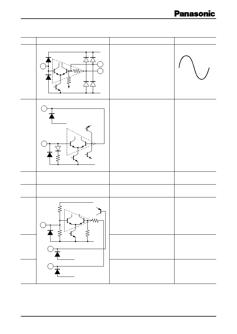
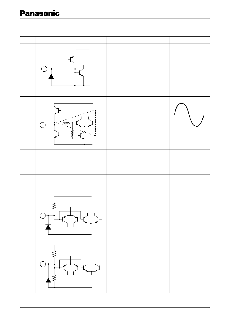
I Terminal Equivalent Circuits
Note) The values mentioned below are the typical ones and is subject to change due to application condition and dispersion of IC.
Pin No.
Equivalent circuit
Description
Waveform (typ.)
1
PB-in (R):
Playback amp. input
DC 0.78 V
AC
-66.2 dBV
2
V
REF
:
DC 0.78 V
Reference voltage output
3
Refer to pin 1
PB-in (L):
Refer to pin 1
Playback amp. input
4
Refer to pin 2
V
REF
-in:
DC 0.78 V
Reference voltage input
5
RF-in:
DC 1.0 V
Ripple filter reference voltage input
6
RF-base:
DC 0.47 V
Ripple filter
7
V
RPF
:
DC 1.13 V
Ripple filter reference voltage output
Pins
26, 28
Pins
25, 27
V
CC
GND
V
REF
Pins
1,3
+
200 k
25 k
2
4
GND
GND
+
5
70 k
350 k
100 k
14 k
+
V
CC
GND
GND
6
GND
7
AN7504SB
5
SDC00029BEB
Pin No.
Equivalent circuit
Description
Waveform (typ.)
8
AGC-TAU:
AGC time constant
9
PWR-out (L):
Power amp. voltage output
DC 0.6 V
AC
-8.8 dBV
10
GND:
0 V
GND pin
11
V
CC
:
1.2 V
Power supply pin
12
Refer to pin 9
PWR-out (R):
Refer to pin 9
Power amp. voltage output
13
STBY, PWR mute CNT:
PWR-mute off
Pin open: V
CC
- V
13
< 0.1 V
PWR-mute on
- 0.2 V < 1/2V
CC
- V
13
< 0.2 V
STBY on
V
13
< 0.1 V
14
FWD/REV/Pre-mute:
FWD/REV/pre-mute control
Pre-mute
Voltage high: V
CC
- 0.1 < V
14-19
FWD
Pin open
REV
Voltage low: V
14-19
< 0.1
8
V
RPF
GND
V
CC
GND
Pins 9, 12
60 k
4 k
+
13
V
RPF
GND
220 k
120 k
14
V
RPF
GND
120 k
I Terminal Equivalent Circuits (continued)
Note) The values mentioned below are the typical ones and is subject to change due to application condition and dispersion of IC.
Document Outline